Posts Tagged ‘recover mcu embedded firmware’
 Recover MCU ATmega861A Code
Recover MCU ATmega861A is a process to unlock microcontroller ATmega861A secured flash and eeprom memory, and then readout the code from ATmega861A;
The EEPROM Read Enable Signal EERE is the read strobe to the EEPROM. When the correct address is set up in the EEAR Register, the EERE bit must be written to a logic one to trigger the EEPROM read. The EEPROM read access takes one instruction, and the requested data is available immediately.
When the EEPROM is read, the CPU is halted for four cycles before the next instruction is executed. The user should poll the EEPE bit before starting the read operation. If a write operation is in progress, it is neither possible to read the EEPROM, nor to change the EEAR Register if Reverse engineering microcontroller attiny85 flash.
The calibrated Oscillator is used to time the EEPROM accesses. Table 3 lists the typical programming time for EEPROM access from the CPU. The following code examples show one assembly and one C function for writing to the EEPROM. The examples assume that interrupts are controlled (e.g. by disabling interrupts globally) so that no interrupts will occur during execution of these functions.
The examples also assume that no Flash Boot Loader is present in the software. If such code is present, the EEPROM write function must also wait for any ongoing SPM command to finish. The next code examples show assembly and C functions for reading the EEPROM after break MCU attiny2313 code.
The examples assume that interrupts are controlled so that no interrupts will occur during execution of these functions. During periods of low VCC, the EEPROM data can be corrupted because the supply voltage is too low for the CPU and the EEPROM to operate properly.
These issues are the same as for board level systems using EEPROM, and the same design solutions should be applied. An EEPROM data corruption can be caused by two situations when the voltage is too low. First, a regular write sequence to the EEPROM requires a minimum voltage to operate correctly when Reverse engineering microcontroller attiny4313 code.
Secondly, the CPU itself can execute instructions incorrectly, if the supply voltage is too low. EEPROM data corruption can easily be avoided by following this design recommendation:
Keep the AVR RESET active (low) during periods of insufficient power supply voltage. This can be done by enabling the internal Brown-out Detector (BOD). If the detection level of the internal BOD does not match the needed detection level, an external low VCC reset Protection circuit can be used.
If a reset occurs while a write operation is in progress, the write operation will be completed provided that the power supply voltage is sufficient.
 Recover MCU ATtiny88A Program
Recover MCU ATtiny88A Program from secured flash memory, unlock microcontroller attiny88a security fuse bit by focus ion beam skill and read the firmware from microprocessor attiny88a memory;
The ATtiny48/88 is a low-power CMOS 8-bit microcontroller based on the AVR enhanced RISC architecture. By executing powerful instructions in a single clock cycle, the ATtiny48/88 achieves throughputs approaching 1 MIPS per MHz allowing the system designer to optimize power consumption versus processing speed.
The AVR core combines a rich instruction set with 32 general purpose working registers. All the 32 registers are directly connected to the Arithmetic Logic Unit (ALU), allowing two independent registers to be accessed in one single instruction executed in one clock cycle if Reverse engineering pic18f248 MCU.
The resulting architecture is more code efficient while achieving throughputs up to ten times faster than conventional CISC microcontrollers. The ATtiny48/88 provides the following features: 4/8K bytes of In-System Programmable Flash, 64/64 bytes EEPROM, 256/512 bytes SRAM, 24 general purpose I/O lines (28 I/Os in 32-lead TQFP and 32-pad QFN/MLF packages).
32 general purpose working registers, two flexible Timer/Counters with compare modes, internal and external interrupts, a byte-oriented 2-wire serial interface, an SPI serial port, a 6-channel 10-bit ADC (8 channels in 32-lead TQFP and 32-pad QFN/MLF packages), a programmable Watchdog Timer with internal oscillator, and three software selectable power saving modes.
Idle mode stops the CPU while allowing Timer/Counters, 2-wire serial interface, SPI port, and interrupt system to continue functioning. Power-down mode saves the register contents but freezes the oscillator, disabling all other MCU functions until the next interrupt or hardware reset. ADC Noise Reduction mode stops the CPU and all I/O modules except ADC, and helps to minimize switching noise during ADC conversions.
The device is manufactured using Atmel’s high density non-volatile memory technology. The On-MCU ISP Flash allows the program memory to be reprogrammed In-System through an SPI serial interface, by a conventional non-volatile memory programmer, or by an on-MCU boot program running on the AVR core.
The boot program can use any interface to download the application program in the Flash memory. By combining an 8-bit RISC CPU with In-System Self-Programmable Flash on a monolithic MCU, the Atmel ATtiny48/88 is a powerful microcontroller that provides a highly flexible and cost effective solution to many embedded control applications.
The ATtiny48/88 AVR is supported by a full suite of program and system development tools including: C compilers, macro assemblers, program debugger/simulators and evaluation kits. This documentation contains simple code examples that briefly show how to use various parts of the device.
These code examples assume that the part specific header file is included before compilation. Be aware that not all C compiler vendors include bit definitions in the header files and interrupt handling in C is compiler dependent. Please confirm with the C compiler documentation for more details.
For I/O Registers located in extended I/O map, “IN”, “OUT”, “SBIS”, “SBIC”, “CBI”, and “SBI” instructions must be replaced with instructions that allow access to extended I/O. Typically “LDS” and “STS” combined with “SBRS”, “SBRC”, “SBR”, and “CBR”.
Reliability Qualification results show that the projected data retention failure rate is much less than 1 PPM over 20 years at 85°C or 100 years at 25°C. Typical values contained in this datasheet are based on simulations and characterization of other AVR microcontrollers manufactured on the same process technology. Min and Max values will be available after the device is characterized.
 Recover MCU ATtiny88V Software
Recover MCU ATtiny88V Software and make the firmware cloning from master attiny88v which will provide the same functions, program from attiny88v memory will be readout by programmer;
The Stack is mainly used for storing temporary data, for storing local variables and for storing return addresses after interrupts and subroutine calls. The Stack Pointer Register always points to the top of the Stack. Note that the Stack is implemented as growing from higher memory locations to lower memory locations when Recover Mcu pic16f628 firmware.
This implies that a Stack PUSH command decreases the Stack Pointer. The Stack Pointer points to the data SRAM Stack area where the Subroutine and Interrupt Stacks are located. This Stack space in the data SRAM must be defined by the program before any subroutine calls are executed or interrupts are enabled.
The Stack Pointer must be set to point above 0x0200. The initial value of the stack pointer is the last address of the internal SRAM. The Stack Pointer is decremented by one when data is pushed onto the Stack with the PUSH instruction, and it is decremented by three when the return address is pushed onto the Stack with subroutine call or interrupt.
The Stack Pointer is incremented by one when data is popped from the Stack with the POP instruction, and it is incremented by three when data is popped from the Stack with return from subroutine RET or return from interrupt RETI after break pic12hv615 Mcu.
The AVR Stack Pointer is implemented as two 8-bit registers in the I/O space. The number of bits actually used is implementation dependent. Note that the data space in some implementations of the AVR architecture is so small that only SPL is needed.
In this case, the SPH Register will not be present. This section describes the general access timing concepts for instruction execution. The AVR CPU is driven by the CPU clock clkCPU, directly generated from the selected clock source for the chip. No internal clock division is used.
Figure 9 shows the parallel instruction fetches and instruction executions enabled by the Harvard architecture and the fast-access Register File concept. This is the basic pipelining concept to obtain up to 1 MIPS per MHz with the corresponding unique results for functions per cost, functions per clocks, and functions per power-unit.
The AVR provides several different interrupt sources. These interrupts and the separate Reset Vector each have a separate program vector in the program memory space. All interrupts are assigned individual enable bits which must be written logic one together with the Global Interrupt Enable bit in the Status Register in order to enable the interrupt.
Depending on the Program Counter value, interrupts may be automatically disabled when Boot Lock bits BLB02 or BLB12 are programmed. This feature improves software security.
The lowest addresses in the program memory space are by default defined as the Reset and Interrupt Vectors. The complete list of vectors is shown in “Interrupts” on page 69. The list also determines the priority levels of the different interrupts. The lower the address the higher is the priority level.
RESET has the highest priority, and next is INT0 – the External Interrupt Request 0. The Interrupt Vectors can be moved to the start of the Boot Flash section by setting the IVSEL bit in the MCU Control Register (MCUCR).
Refer to “Interrupts” on page 69 for more information. The Reset Vector can also be moved to the start of the Boot Flash section by programming the BOOTRST Fuse. When an interrupt occurs, the Global Interrupt Enable I-bit is cleared and all interrupts are disabled.
The user software can write logic one to the I-bit to enable nested inter rupts. All enabled interrupts can then interrupt the current interrupt routine. The I-bit is automatically set when a Return from Interrupt instruction – RETI – is executed.
 Recover MCU ATtiny48 Heximal
Recover MCU ATtiny48 Heximal from embedded flash and eeprom memory, unlock microcontroller attiny48 tamper resistance system and then copy the firmware from original attiny48 to the new MCU units;
During interrupts and subroutine calls, the return address Program Counter (PC) is stored on the Stack. The Stack is effectively allocated in the general data SRAM, and consequently the Stack size is only limited by the total SRAM size and the usage of the SRAM when Recover chip pic16c77 code.
All user programs must initialize the SP in the Reset routine (before subroutines or interrupts are executed). The Stack Pointer (SP) is read/write accessible in the I/O space. The data SRAM can easily be accessed through the five different addressing modes supported in the AVR architecture.
The memory spaces in the AVR architecture are all linear and regular memory maps. A flexible interrupt module has its control registers in the I/O space with an additional Global Interrupt Enable bit in the Status Register. All interrupts have a separate Interrupt Vector in the Interrupt Vector table when break pic16f636 Mcu.
The interrupts have priority in accordance with their Interrupt Vector position. The lower the Interrupt Vector address, the higher the priority. The I/O memory space contains 64 addresses for CPU peripheral functions as Control Registers, SPI, and other I/O functions.
The I/O Memory can be accessed directly, or as the Data Space locations following those of the Register File, 0x20 – 0x5F. In addition, the ATtiny48 has Extended I/O space from 0x60 – 0x1FF in SRAM where only the ST/STS/STD and LD/LDS/LDD instructions can be used after copy microcontroller pic16f767 program.
The high-performance AVR ALU operates in direct connection with all the 32 general purpose working registers. Within a single clock cycle, arithmetic operations between general purpose registers or between a register and an immediate are executed.
The ALU operations are divided into three main categories – arithmetic, logical, and bit-functions. Some implementations of the architecture also provide a powerful multiplier supporting both signed/unsigned multiplication and fractional format. See the “Instruction Set” section for a detailed description.
The Status Register contains information about the result of the most recently executed arithmetic instruction. This information can be used for altering program flow in order to perform conditional operations. Note that the Status Register is updated after all ALU operations, as specified in the Instruction Set Reference.
This will in many cases remove the need for using the dedicated compare instructions, resulting in faster and more compact code. The Status Register is not automatically stored when entering an interrupt routine and restored when returning from an interrupt. This must be handled by software.
 Recover MCU ATmega2561V Eeprom
Recover MCU ATmega2561V Eeprom content needs to crack mcu atmega2561v protective system by focus ion beam and then copy the firmware inside flash and eeprom memory of microcontroller atmega2561v to new ones for same functionality;
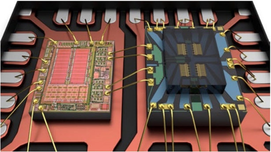
This documentation contains simple code examples that briefly show how to use various parts of the device. Be aware that not all C compiler vendors include bit definitions in the header files and interrupt handling in C is compiler dependent. Please confirm with the C compiler documentation for more details.
These code examples assume that the part specific header file is included before compilation. For I/O registers located in extended I/O map, “IN”, “OUT”, “SBIS”, “SBIC”, “CBI”, and “SBI” instructions must be replaced with instructions that allow access to extended I/O. Typically “LDS” and “STS” combined with “SBRS”, “SBRC”, “SBR”, and “CBR” if Recover atmega2560 MCU flash.
This section discusses the AVR core architecture in general. The main function of the CPU core is to ensure correct program execution. The CPU must therefore be able to access memories, perform calculations, control peripherals, and handle interrupts.
In order to maximize performance and parallelism, the AVR uses a Harvard architecture – with separate memories and buses for program and data. Instructions in the program memory are executed with a single level pipelining. While one instruction is being executed, the next instruction is pre-fetched from the program memory.
This concept enables instructions to be executed in every clock cycle. The program memory is In-System Reprogrammable Flash memory. The fast-access Register File contains 32 x 8-bit general purpose working registers with a single clock cycle access time.
This allows single-cycle Arithmetic Logic Unit (ALU) operation. In a typical ALU operation, two operands are output from the Register File, the operation is executed, and the result is stored back in the Register File – in one clock cycle if Reverse engineering atmega1281 MCU.
Six of the 32 registers can be used as three 16-bit indirect address register pointers for
Data Space addressing – enabling efficient address calculations. One of the these address pointers can also be used as an address pointer for look up tables in Flash program memory. These added function registers are the 16-bit X-, Y-, and Z-register, described later in this section.
The ALU supports arithmetic and logic operations between registers or between a constant and a register. Single register operations can also be executed in the ALU. After an arithmetic operation, the Status Register is updated to reflect information about the result of the operation.
Program flow is provided by conditional and unconditional jump and call instructions, able to directly address the whole address space. Most AVR instructions have a single 16-bit word format. Every program memory address contains a 16- or 32-bit instruction.
Program Flash memory space is divided in two sections, the Boot Program section and the Application Program section. Both sections have dedicated Lock bits for write and read/write protection. The SPM instruction that writes into the Application Flash memory section must reside in the Boot Program section.
 Recover MCU PIC16F628 Firmware
Recover MCU PIC16F628 Firmware needs to unlock microcontroller pic16f628 protective memory and then readout embedded firmware from mcu pic16f628 flash memory;
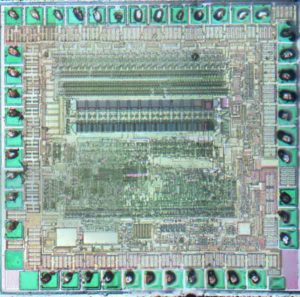
We can Recover MCU PIC16F628 Firmware, please view the MCU PIC16F628 features for your reference:
The PIC16F62X are 18-Pin FLASH-based members of the versatile PIC16CXX family of low-cost, high-performance, CMOS, fully-static, 8-bit microcontrollers. All PICmicro® microcontrollers employ an advanced RISC architecture.
The PIC16F62X have enhanced core features, eight-level deep stack, and multiple internal and external interrupt sources. The separate instruction and data buses of the Harvard architecture allow a 14-bit wide instruction word with the separate 8-bit wide data.
The two-stage instruction pipeline allows all instructions to execute in a single-cycle, except for program branches (which require two cycles). A total of 35 instructions (reduced instruction set) are available. Additionally, a large register set gives some of the architectural innovations used to achieve a very high performance.
PIC16F62X microcontrollers typically achieve a 2:1 code compression and a 4:1 speed improvement over other 8-bit microcontrollers in their class. PIC16F62X devices have special features to reduce external components, thus reducing system cost, enhancing system reliability and reducing power consumption.
There are eight oscillator configurations, of which the single pin ER oscillator provides a low-cost solution. The LP oscillator minimizes power consumption, XT is a standard crystal, INTRC is a self-contained internal oscillator and the HS is for High Speed crystals.
The SLEEP (power-down) mode offers power savings. The user can wake up the chip from SLEEP through several external and internal interrupts and reset.
A highly reliable Watchdog Timer with its own on-chip RC oscillator provides protection against software lock- up.
Table 1-1 shows the features of the PIC16F62X mid-range microcontroller families. A simplified block diagram of the PIC16F62X is shown in Figure 3-1.
The PIC16F62X series fits in applications ranging from battery chargers to low-power remote sensors. The FLASH technology makes customization of application programs (detection levels, pulse generation, timers, etc.) extremely fast and convenient.
The small footprint packages make this microcontroller series ideal for all applications with space limitations. Low-cost, low-power, high-performance, ease of use and I/O flexibility make the PIC16F62X very versatile.
The PIC16F62X family is supported by a full-featured macro assembler, a software simulator, an in-circuit emulator, a low-cost development programmer and a full-featured programmer. A Third Party “C” compiler support tool is also available.