Posts Tagged ‘recover chip firmware’
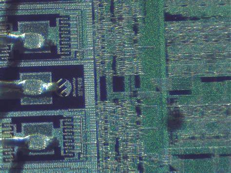
 Recover Chip PIC12C509A Firmware
Recover Chip PIC12C509A Firmware from embedded memory, the program and data can be extracted from pic12c509a mcu and read out from secured microcontroller pic12c509a memory;

The same majority voting is done to the stop bit as done for the other bits in the frame. If the stop bit is registered to have a logic 0 value, the Frame Error (FEn) Flag will be set.
A new high to low transition indicating the start bit of a new frame can come right after the last of the bits used for majority voting. For Normal Speed mode, the first low level sample can be at point marked (A) in Figure 89 if Recover mcu stm32f107rct6 code firmware.
For Double Speed mode the first low level must be delayed to (B). (C) marks a stop bit of full length. The early start bit detection influences the operational range of the Receiver.
The operational range of the Receiver is dependent on the mismatch between the received bit rate and the internally generated baud rate after copy microcontroller pic16f684 memory.
If the Transmitter is sending frames at too fast or too slow bit rates, or the internally generated baud rate of the Receiver does not have a similar (see Table 99) base frequency, the Receiver will not be able to synchronize the frames to the start bit.
The following equations can be used to calculate the ratio of the incoming data rate and internal receiver baud rate. Sum of character size and parity size (D = 5 to 10 bit) Samples per bit. S = 16 for Normal Speed mode and S = 8 for Double Speed mode.
First sample number used for majority voting. SF = 8 for normal speed and SF = 4 for Double Speed mode. Middle sample number used for majority voting.
SM = 9 for normal speed and
SM = 5 for Double Speed mode.
Rslow is the ratio of the slowest incoming data rate that can be accepted in relation to the receiver baud rate. Rfast is the ratio of the fastest incoming data rate that can be accepted in relation to the receiver baud rate. Table 99 and Table 100 list the maximum receiver baud rate error that can be tolerated. Note that Normal Speed mode has higher toleration of baud rate variations after extract mcu pic16f54c hex.
 Recovery Chip ATMEGA2560PV Program
We can Recovery CHIP ATMEGA2560PV Program, please view the CHIP ATMEGA2560PV features for your reference:
In this example, Timer/Counter2 provides the carrier, while the modulating signal is generated by the Output Compare unit C of the Timer/Counter1 when Recovery CHIP program.
The resolution of the PWM signal (OC1C) is reduced by the modulation. The reduction factor is equal to the number of system clock cycles of one period of the carrier (OC0A).
In this example the resolution is reduced by a factor of two. The reason for the reduction is illustrated in Figure 66 at the second and third period of the PB7 output when PORTB7 equals zero if Recovery CHIP program.
The period 2 high time is one cycle longer than the period 3 high time, but the result on the PB7 output is equal in both periods. Timer/Counter2 is a general purpose, single channel, 8-bit Timer/Counter module. The main features are before Recovery CHIP program:
Single Channel Counter
Clear Timer on Compare Match (Auto Reload)
Glitch-free, Phase Correct Pulse Width Modulator (PWM) after Recovery CHIP program
Frequency Generator
10-bit Clock Prescaler
Overflow and Compare Match Interrupt Sources (TOV2, OCF2A and OCF2B)
Allows Clocking from External 32 kHz Watch Crystal Independent of the I/O Clock
A simplified block diagram of the 8-bit Timer/Counter is shown in Figure 60.. For the actual placement of I/O pins, see “Pin Configurations” on page 2. CPU accessible I/O Registers, including I/O bits and I/O pins, are shown in bold. The device-specific I/O Register and bit locations are listed in the “8-bit Timer/Counter Register Description” on page 184 if Recovery CHIP program.
The Power Reduction Timer/Counter2 bit, PRTIM2, in “Power Reduction Register 0 – PRR0” on page 54 must be written to zero to enable Timer/Counter2 module before Recovery CHIP program.
The Timer/Counter (TCNT2) and Output Compare Register (OCR2A and OCR2B) are 8-bit registers. Interrupt request (abbreviated to Int.Req.) signals are all visible in the Timer Interrupt Flag Register (TIFR2). All interrupts are individually masked with the Timer Interrupt Mask Register (TIMSK2). TIFR2 and TIMSK2 are not shown in the figure when Recovery CHIP program.
The Timer/Counter can be clocked internally, via the prescaler, or asynchronously clocked from the TOSC1/2 pins, as detailed later in this section. The asynchronous operation is controlled by the Asynchronous Status Register (ASSR). The Clock Select logic block controls which clock source the Timer/Counter uses to increment (or decrement) its value. The Timer/Counter is inactive when no clock source is selected. The output from the Clock Select logic is referred to as the timer clock (clkT2). The double buffered Output Compare Register (OCR2A and OCR2B) are compared with the Timer/Counter value at all times after Recovery CHIP program.
The result of the compare can be used by the Waveform Generator to generate a PWM or variable frequency output on the Output Compare pins (OC2A and OC2B). See “Output Compare Unit” on page 175. for details.
The compare match event will also set the Compare Flag (OCF2A or OCF2B) which can be used to generate an Output Compare interrupt request. Many register and bit references in this document are written in general form. A lower case “n” replaces the Timer/Counter number, in this case 2. However, when using the register or bit defines in a program, the precise form must be used, i.e., TCNT2 for accessing Timer/Counter2 counter value and so on before Recovery CHIP program.
The definitions in Table 84 are also used extensively throughout the section.