Posts Tagged ‘pcba redesign’
 PCB Redesign
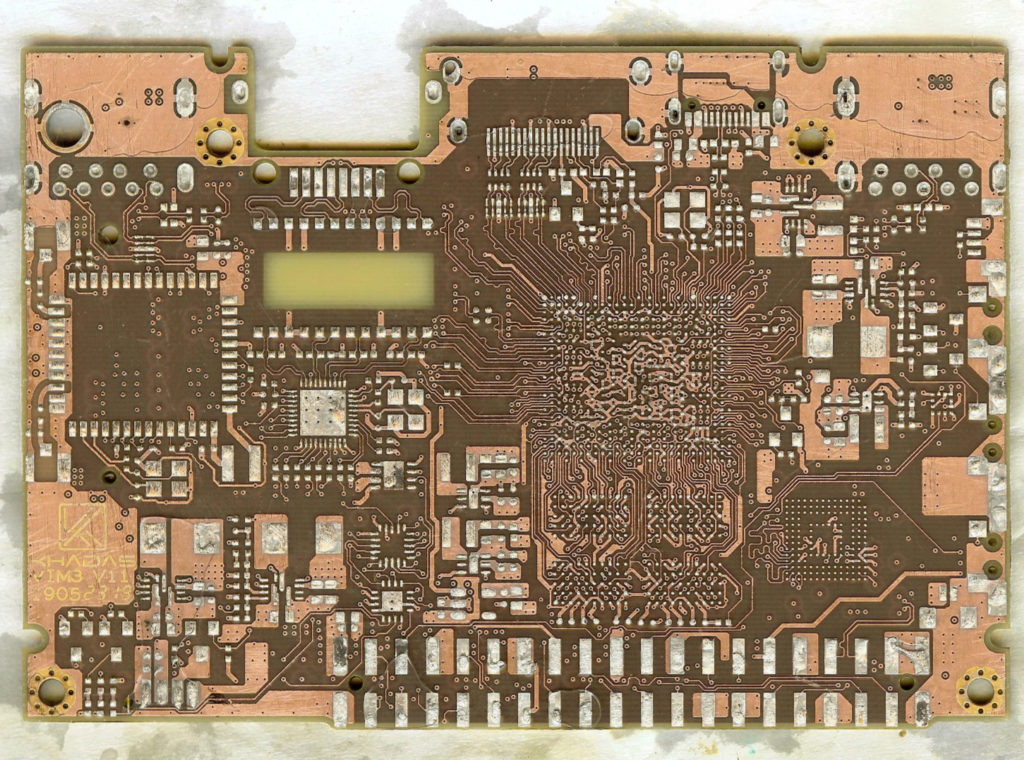
The Problem why the PCB Redesign occurs is because the original Printed circuit board layout drawing and gerber file need to be modified which can be fulfilled by extract wiring diagram of circuit board;

Do you have legacy circuit board layouts that were created with an obsolete CAD system? Many times these layouts are still being used to maintain current products or as replacement parts for older products. Do you frequently have to redesign PCB board layouts for a better emc performance? Do you have to transfer these layouts from one manufacturing platform to another? Are you looking at a complete PCB drawing recreation to facilitate this?
The Solution which PCB Redesign can bring:
As an alternate solution to PCB reverse engineering or Gerber modification is to “Reverse Engineering” the Gerber files into an intelligent format that can be read by today’s PCB CAD systems. This process takes the Gerber artwork, builds intelligence and electrical nets and ends in a complete CAD database which ensures a pefect match with the original circuit layout.