Posts Tagged ‘pcb card reverse engineering service’
 PCB Reverse Engineering Analysis and Instruction Process
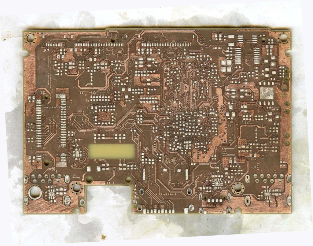
PCB Reverse Engineering analysis and instruction process can help to ensure the PCB board drawing documents correctiveness, the extracted schematic diagram and PCB gerber file can be used to reproduce the circuit board;

PCB Reverse Engineering’s Analysis and Instruction Process
a Functional/economic analysis should be completed to collect available documentation, determine missing data requirements, determine testing requirements, and develop the PCB Reverse Engineering service cost-Estimates and Schedules;
b. A disassembly procedure should be completed for each candidate to ensure functional integrity is maintained to allow for a viable analysis and documentation;
c. A PCB cloning service management plan should be completed for each candidate to ensure a logical sequence of events to prevent delays or misinterpretations in the overall program objectives;
d. A hardware analysis should be performed to develop the missing data required for Level 3 drawings which can be restored from embeded microcontroller memory;
e. Level 3 drawings are the result of the PCB reverse engineering service process and contain the documented parameters necessary to reproduce the selected candidate;
f. A quality control study should be performed and documented on the Level 3 drawings and prototypes of candidates to certify their compliance with original candidate specifications;
g. A production review should be performed to determine the economics of production of the electronic card reverse engineering service item;
h. Prototype production involves the manufacture and testing of prototypes to determine if they meet all required specifications; and
i. A finalized TDP should be formulated and delivered to the government/Tasking Agency requesting the PCB board copying service of the candidate item.