Posts Tagged ‘brechen gesicherter Mikroprozessor-Firmware-Code’
 Locked MCU ATMEGA32M1 Firmware Recovery
Locked MCU ATMEGA32M1 Firmware Recovery needs to unlock atmega32m1 microcontroller flash memory, then readout embedded software from atmega32m1 processor;
To drive the device from an external clock source, XTAL1 should be driven as shown in below Figure. To run the device on an external clock, the CKSEL Fuses must be programmed to “0000”. By programming the CKOPT Fuse, the user can enable an internal 36 pF capacitor between XTAL1 and GND, and XTAL2 and GND.
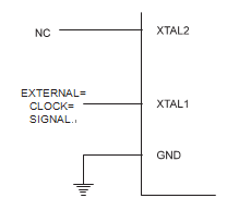
When applying an external clock, it is required to avoid sudden changes in the applied clock frequency to ensure stable operation of the MCU. A variation in frequency of more than 2% from one clock cycle to the next can lead to unpredictable behavior in the process of breaking atmega16l locked mcu flash memory. It is required to ensure that the MCU is kept in Reset during such changes in the clock frequency.
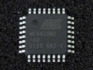
a recuperação de firmware MCU ATMEGA32M1 bloqueada precisa desbloquear a memória flash do microcontrolador atmega32m1 e, em seguida, ler o software incorporado do processador atmega32m1;
For AVR microcontrollers with Timer/Counter Oscillator pins (TOSC1 and TOSC2), the crystal is connected directly between the pins. By programming the CKOPT Fuse, the user can enable internal capacitors on XTAL1 and XTAL2 to recover microprocessor atmega16 protective flash, thereby removing the need for external capacitors. The Oscillator is optimized for use with a 32.768 kHz watch crystal. Applying an external clock source to TOSC1 is not recommended.
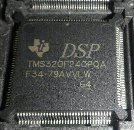
 Break DSP Microcontroller TMS320F240 Locked Flash Memory
Break DSP Microcontroller TMS320F240 Locked Flash Memory and extract embedded IC code from its flash memory, clone extracted firmware to new MCU tms320f240pg for perfect cloning;
| LOWERCASE SUBSCRIPTS AND THEIR MEANINGS: LETTERS AND SYMBOLS AND THEIR MEANINGS: |
Timing parameter symbols used are created in accordance with JEDEC Standard 100. To shorten the symbols, some of the pin names and other related terminology have been abbreviated as follows:
a access time
H High
- cycle time (period) L Low
- delay time V Valid
f fall time X Unknown, changing, or don’t care level
h hold time Z High impedance r rise time
su setup time
t transition time
- valid time
- pulse duration (width)
All output signals from the 28x devices (including XCLKOUT) are derived from an internal clock such that all output transitions for a given half-cycle occur with a minimum of skewing relative to each other when break dsp mcu tms320f28063 flash memory.
The signal combinations shown in the following timing diagrams may not necessarily represent actual cycles. For actual cycle examples, see the appropriate cycle description section of this document.
This test load circuit is used to measure all switching characteristics provided in this document.
