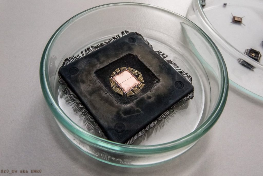
Reverse Locked IC PIC16F54 manufacturing process and extract IC PIC16F54 Firmware from secured program and data memory by cracking PIC16F54 eeprom and flash memory;

The output driver control register is loaded with the contents of the W register by executing the TRIS instruction. A ‘1’ from a TRIS register bit puts the corresponding output driver in a hi-impedance mode.
A ‘0’ puts the contents of the output data latch on the selected pins, enabling the output buffer. The exceptions are GP3 which is input only and GP2 which may be controlled by the option register,
A read of the ports reads the pins, not the output data latches. That is, if an output driver on a pin is enabled and driven high, but the external system is holding it low, a read of the port will indicate that the pin is low.
The TRIS registers are “write-only” and are set (output drivers disabled) upon RESET. Some instructions operate internally as read followed by write operations after Recover IC PIC12LC508A eeprom.
The BCF and BSF instructions, for example, read the entire port into the CPU, execute the bit operation and re-write the result. Caution must be used when these instructions are applied to a port example.
a BSF operation on bit5 of GPIO will cause directional I/O pin (say bit0) and it is defined as an input at this time, the input signal present on the pin itself would be read into the CPU and rewritten to the data latch of this particular pin, overwriting the where one or more pins are used as input/outputs if copy protected chip pic16c56 code.
For previous content. As long as the pin stays in the input mode, no problem occurs. However, if bit0 is switched into output mode later on, the content of the data latch maybe unknown.
