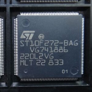
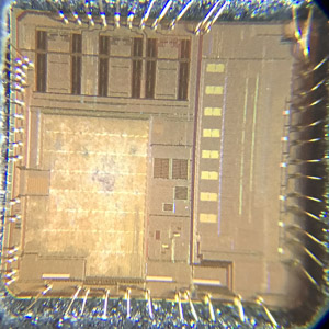
 Reverse Engineering ST10F272M-4QR3 Encrypted Microprocessor Memory
Reverse Engineering ST10F272M-4QR3 Encrypted Microprocessor Memory can help designer to recover embedded flash content of microcontroller st10f272m-4qr3 and clone flash program in the format of binary or heximal to new MCU ST10F272M-4QR3;

Reverse Engineering ST10F272M-4QR3 Encrypted Microprocessor Memory can help designer to recover embedded flash content of microcontroller st10f272m-4qr3 and clone flash program in the format of binary or heximal to new MCU ST10F272M-4QR3;
Output transition is not programmable.
CAN module is enhanced: ST10F273 implements two C-CAN modules, so the programming model is slightly different. Besides, the possibility to map in parallel the two CAN modules is added (on P4.5/P4.6).
On-chip main oscillator input frequency range has been reshaped, reducing it from 1 to 25 MHz down to 4 to 12 MHz. This is a low power oscillator amplifier, that allows a power consumption reduction when Real Time Clock is running in Power down mode, using as reference the on-chip main oscillator clock. When this on-chip amplifier is used as reference for Real Time Clock module, the Power-down consumption is dominated by the consumption of the oscillator amplifier itself.

зворотне проектування ST10F272M зашифрована захисна система мікропроцесора для зчитування вбудованого мікропрограмного забезпечення з флеш-пам’яті може допомогти розробнику відновити флеш-вміст двійкового файлу та шістнадцяткових даних з мікроконтролера ST10F272M
A second on-chip oscillator amplifier circuit (32 kHz) is implemented for low power modes: it can be used to provide the reference to the Real Time Clock counter (either in Power down or Stand-by mode). Pin XTAL3 and XTAL4 replace a couple of VDD/VSS pins of ST10F272M-4QR3.

visszafejtés Az ST10F272M titkosított mikroprocesszoros védelmi rendszer a beágyazott firmware flash memóriából történő kiolvasásához segíthet a tervezőnek a bináris fájlok flash tartalmának és a heximális adatoknak az ST10F272M mikrokontrollerről történő helyreállításában
8-bit bidirectional I/O port, bit-wise programmable for input or output via direction bit. Programming an I/O pin as input forces the corresponding output driver to high impedance state. Port 6 outputs can be configured as push-pull or open drain drivers. The input threshold of Port 6 is selectable (TTL or CMOS). The following Port 6 pins have alternate functions:
External access enable pin.
A low level applied to this pin during and after Reset forces the ST10F273 to start the program from the external memory space. A high level forces ST10F273 to start in the internal memory space. This pin is also used (when Stand-by mode is entered, that is ST10F273 under reset and main VDD turned off) to bias the 32 kHz oscillator amplifier circuit and to provide a reference voltage for the low-power embedded voltage regulator which generates the internal 1.8V supply for the RTC module (when not disabled) and to retain data inside the Stand-by portion of the XRAM (16Kbyte).

engenharia reversa O sistema de proteção do microprocessador criptografado ST10F272M para ler o firmware incorporado da memória flash pode ajudar o designer a recuperar o conteúdo flash do arquivo binário e dados heximais do microcontrolador ST10F272M
It can range from 4.5 to 5.5V (6V for a reduced amount of time during the device life, 4.0V when RTC and 32 kHz on-chip oscillator amplifier are turned off). In running mode, this pin can be tied low during reset without affecting 32 kHz oscillator, RTC and XRAM activities, since the presence of a stable VDD guarantees the proper biasing of all those modules.