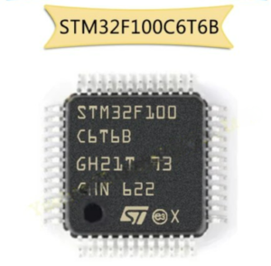
 Reverse Engineer STMicrco ARM MCU STM32F100C6
Reverse Engineer STMicrco ARM MCU STM32F100C6 needs to unlock stm32f100c6’s security fuse bit and then extract embedded firmware from microcontroller’s flash and eeprom memory;

The STM32F100xx value line family incorporates the high-performance ARM Cortex™-M3 32-bit RISC core operating at a 24 MHz frequency which will be useful for Unlock ARM MCU STM32F100C6 Memory, high-speed embedded memories (Flash memory up to 128 Kbytes and SRAM up to 8 Kbytes), and an extensive range of enhanced peripherals and I/Os connected to two APB buses.

रिवर्स इंजीनियरिंग एसटीमाइक्रोको एआरएम एमसीयू STM32F100C6 को STM32F100C6 के सुरक्षा फ्यूज बिट को अनलॉक करने और फिर माइक्रोकंट्रोलर के फ्लैश और ईप्रोम मेमोरी से एम्बेडेड फर्मवेयर निकालने, समीपस्थ या बाइनरी के फर्मवेयर स्रोत कोड को नए माइक्रोकंट्रोलर STM32F100C6 में कॉपी करने की आवश्यकता होती है;
All devices offer standard communication interfaces (up to two I2Cs, two SPIs, one HDMI CEC, and up to three USARTs), one 12-bit ADC, two 12-bit DACs, up to six general-purpose 16-bit timers and an advanced-control PWM timer for the purpose of MCU source code reverse engineering.
The STM32F100xx low- and medium-density value line family operates in the –40 to +85 °C and –40 to +105 °C temperature ranges, from a 2.0 to 3.6 V power supply. A comprehensive set of power-saving mode allows the design of low-power applications.

الهندسة العكسية STMicrco ARM MCU STM32F100C6 يحتاج إلى فتح بت الصمامات الأمنية STM32F100C6 ثم استخراج البرامج الثابتة المضمنة من فلاش متحكم دقيق وذاكرة EEPROM ، ونسخ شفرة مصدر البرامج الثابتة من heximal أو ثنائي إلى متحكم دقيق جديد STM32F100C6 ؛
The STM32F100xx value line family includes devices in three different packages ranging from 48 pins to 100 pins. Depending on the device chosen, different sets of peripherals are included, the description below gives an overview of the complete range of peripherals proposed in this family from the process of Crack Microcontroller IC TI 430G2452.
These features make the STM32F100xx value line microcontroller family from the process of Attack Microcontroller MCU Microchip PIC16F84A suitable for a wide range of applications:
Application control and user interface
Medical and handheld equipment
PC peripherals, gaming and GPS platforms
Industrial applications: PLC, inverters, printers, and scanners
Alarm systems, Video intercom, and HVAC