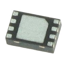
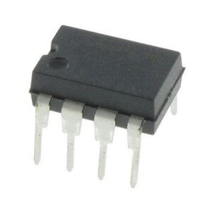
Replicate PIC12F519 Microprocessor Flash Program can help engineer to unlock ic chip secured pic12f519 binary from its flash memory, to readout microchip locked pic12f519 source code;

Çoğaltma PIC12F519 Mikroişlemci Flash Programı, mühendisin ic çip korumalı pic12f519 ikili dosyasını flash belleğinden açmasına, mikroçip kilitli pic12f519 kaynak kodunu okumasına yardımcı olabilir
The LVD module has an additional feature that allows the user to supply the trip voltage to the module from an external source. This mode is enabled when bits, LVDL3:LVDL0, are set to ‘1111’. In this state, the com- parator input is multiplexed from the external input pin when breaking microcontroller pic12f629 flash, LVDIN (Figure 18-3). This gives users flexibility, because it allows them to configure the Low-Voltage Detect interrupt to occur at any voltage in the valid operating range.

Kilitli mikrodenetleyici PIC12F519’un kurcalamaya karşı direnç sistemini kırma ve PIC12F519 MCU flash bellekten onaltılık dosyayı kurtarma;
bit 7-6 Unimplemented: Read as ‘0’
bit 5 IRVST: Internal Reference Voltage Stable Flag bit
1 = Indicates that the Low-Voltage Detect logic will generate the interrupt flag at the specified voltage range
0 = Indicates that the Low-Voltage Detect logic will not generate the interrupt flag at the specified volt- age range and the LVD interrupt should not be enabled by breaking dspic30f4011 mcu flash memory;
bit 4 LVDEN: Low-Voltage Detect Power Enable bit
1 = Enables LVD, powers up LVD circuit
0 = Disables LVD, powers down LVD circuit
bit 3-0 LVDL<3:0>: Low-Voltage Detection Limit bits(1)
1111 = External analog input is used (input comes from the LVDIN pin)
1110 = 4.04V-5.15V
1101 = 3.76V-4.79V
1100 = 3.58V-4.56V
1011 = 3.41V-4.34V
1010 = 3.23V-4.11V
1001 = 3.14V-4.00V
1000 = 2.96V-3.77V
0111 = 2.70V-3.43V
0110 = 2.53V-3.21V
0101 = 2.43V-3.10V
0100 = 2.25V-2.86V
0011 = 2.16V-2.75V
0010 = 1.99V-2.53V
0001 = Reserved
0000 = Reserved
Note 1: LVDL<3:0> modes, which result in a trip point below the valid operating voltage of the device, are not tested.
