 REC issues convertible bond loan
Norwegian solar company REC, Renewable Energy Company ASA, proposes to improve its debt maturity profile through issuing a new convertible bond loan maturing in 2018.
REC ASA has mandated Arctic Securities ASA to explore the potential issuance of up to USD 110 million (NOK 643 million) in principal amount of convertible bonds with maturity on September 13, 2018.
In conjunction with the issue of the New Convertible Bond Loan, REC ASA will offer to repurchase and exchange bonds in the Company’s Subordinated Unsecured Convertible Bond Issue 2009/2014 for a principal amount of up to EUR 112 million (NOK 876 million), including accrued interest since the July 4, 2013 interest payment date.
PCB Manufacturer Found Guilty of ITAR Violations
A Woodinville, Wash. company contracted by the U.S. Navy to manufacture high-tech components, and the company’s owner recently pleaded guilty to violating the Arms Export Control Act, according to an ICP slog post.
The owner of Precision Image Corporation admitted to illegally sending restricted U.S. Navy technical information to a Taiwanese printed board (PCB) manufacturer that was subcontracted to make the printed boards.
The information sent to the Taiwanese PCB manufacturer contained the technical specifications for the printed boards – information listed on the United States Munitions List (USML) and controlled by U.S. International Traffic in Arms Regulations (ITAR) and therefore prohibited from being transmitted outside the U.S. without a license from the State Department.
For the past two years, IPC has been promoting a better understanding of ITAR’s applicability to PCBs in order to protect national security. Launched in July 2012, IPC’s Follow the Law, Protect the Board initiative sought to raise awareness and promote compliance with federal regulations on the export of printed boards designed for ITAR-controlled equipment.
Read more: http://evertiq.com/news/32203
German component distribution market grows again
The German component distribution market (according to FBDi eV) grew during the second quarter of 2013 with 2.3%. Orders registered above-average growth.
The state of the German component distribution market is beginning to improvements. According to the FBDi, sales figures increased for the second quarter with 2.3 percent to EUR 712 million compared to the same quarter 2012. The book-to-bill ratio stood at 1.02 (0.96 for the same period last year). The first half ended almost balanced – both turnover and order intake stood at EUR 1.44 billion – which is a promising sign for the second half of the year.
When considering the various component groups, figures for the semiconductor segment have a lot to be desired for: a meager growth of 0.7% to EUR 484 million in turnover. However, order intake was up 8.5% and stood at EUR 497 million. This results in a market share (total component distribution market) of 68%.
This is followed by passive components with a turnover increase of 6.9% to EUR 108 million (representing a 15% market share). With an increase of 3.4% to EUR 75 million in turnover, the segment Electromechanical reached a market share of over 10%. The rest is split between displays, power supplies and sensors.
Read more: http://evertiq.com/news/32198
Reverse LATTICE CPLD Source code
Reverse LATTICE CPLD source code is a process to extract jed file from encrypted Lattice CPLD, using physical MCU invasive cracking method include decapsulation and focus ion beam can help to fulfill the task;
Reverse LATTICE CPLD source code is a process to extract jed file from encrypted Lattice CPLD, using physical MCU invasive cracking method include decapsulation and focus ion beam can help to fulfill the task
The same memory type but built with newer technologies such as 0.9 µm in the Microchip PIC16CR57 microcontroller [124] and 1.0 µm in the Motorola MC68HC705C9A microcontroller [23] requires deprocessing because the top bit-line metal wires obstruct observation of the transistors.
NAND Mask ROM memory type with metal layer programming was used in the NEC µPD78F9116 microcontroller [125] fabricated with 0.35 µm technology. As all the internal layers were planarised, deeper layers cannot be observed unless the top metal layer is removed.
This was accomplished by using Nitrox etching for the passivation layer followed by treatment in a 33% water solution of KOH to etch the top aluminium metal layer but preserving the interconnection layer which is probably made out of tungsten (because when the HCl solution was used to etch the top metal layer, the interconnection layer was etched away as well).
Reverse DSP CPLD IC Chip Program
Reverse DSP CPLD IC Chip Program from memory, and copy memory content to new CPLD chip which will provide the same functions as original DSP chip by Crack CPLD protection.
Reverse DSP CPLD IC Chip Program from memory, and copy memory content to new CPLD chip which will provide the same functions as original DSP chip by Crack CPLD protection
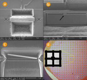
Layout reconstruction requires the images of all the layers inside the chip to be combined. The images are normally taken automatically using a motorised stage to move the sample and special software to combine all the images together.
Normally, for semiconductor chips fabricated with 0.13 µm or smaller technology, images are created using a SEM which has a resolution better than 10 nm.
Read Lattice CPLD embeded firmware
Read Lattice CPLD embeded firmware from locked memory, the file format of CPLD can be JED, unlock CPLD tamper resistance system by cut off the security fuse.
Read Lattice CPLD embeded firmware from locked memory, the file format of CPLD can be JED, unlock CPLD tamper resistance system by cut off the security fuse
The main disadvantage of high resolution microscopes is the short working distance between the objective and a specimen, especially at high magnifications (about 0.3 mm with 100× objective). As a result partially decapsulated chips cannot be observed and full decapsulation of the die is required. Using microscopes with a long working distance, for example the Mitutoyo FS70 [121] with 13 mm working distance on 200× objective, helps solve this problem but at a cost: the resolution is at most 0.4 µm because the NA cannot be high.
Another problem of the high-resolution objectives is a very short depth of focus, which makes the out-of-focus planes look blurred, thus reducing the image quality. This is more noticeable on multilayer chips where the distance between the top and the bottom layer is more than 1 µm.
Confocal microscopy reduces this effect as all out-of-focus planes become dark or appear in different colours depending from their depth. Such confocal systems are very expensive, especially the ones that use laser scanning, and therefore can be afforded by relatively large labs only. Even second-hand confocal microscopes start from £10,000.
Reverse Microchip PIC18F2220 MCU Flash Program
Reverse Microchip PIC18F2220 MCU Flash Program
During interrupts and subroutine calls, the return address PC is stored on the Stack. The Stack is effectively allocated in the general data SRAM, and consequently the Stack size is only limited by the total SRAM size and the usage of the SRAM from Reverse Microchip PIC18F2220 MCU Flash Program. After reset the Stack Pointer (SP) points to the highest address in the internal SRAM.
The SP is read/write accessible in the I/O memory space, enabling easy implementation of multiple stacks or stack areas. The data SRAM can easily be accessed through the five different addressing modes supported in the AVR CPU.The AVR architecture has two main memory spaces, the Program Memory and the Data Memory.
In addition, the XMEGA A3 features an EEPROM Memory for non-volatile data storage. All three memory spaces are linear and require no paging. The available memory size configurations are shown in ”Ordering Information” on page 2. In addition each device has a Flash memory signature row for calibration data, device identification, serial number etc. Non-volatile memory spaces can be locked for further write or read/write operations.
This prevents unrestricted access to the application software. The XMEGA A3 devices contains On-chip In-System Programmable Flash memory for program storage, see Figure 7-1 on page 10. Since all AVR instructions are 16- or 32-bits wide, each Flash address location is 16 bits. The Program Flash memory space is divided into Application and Boot sections.
Reverse Microchip PIC18F2220 MCU Flash Program
Both sections have dedicated Lock Bits for setting restrictions on write or read/write operations. The Store Program Memory (SPM) instruction must reside in the Boot Section when used to write to the Flash memory before the code.
A third section inside the Application section is referred to as the Application Table section which has separate Lock bits for storage of write or read/write protection. The Application Table section can be used for storing non-volatile data or application software from MCU CRACK.
Copy Encrypted Microchip PIC18F2330 Heximal
Copy Encrypted Microchip PIC18F2330 Heximal
The Flash Program Memory and firmware data memory are organized in pages which can be Copy Encrypted Microchip PIC18F2330 Heximal. The pages are word accessible for the Flash and byte accessible for the firmware. Table 7-2 on page 14 shows the Flash Program Memory organization.
Flash write and erase operations are performed on one page at a time, while reading the Flash is done one byte at a time. For Flash access the Z-pointer (Z[m:n]) is used for addressing. The most significant bits in the address (FPAGE) gives the page number and the least significant address bits (FWORD) gives the word.
Table 7-3 on page 14 shows firmware memory organization for the PIC18F2320 devices. Efirmware write and erase operations can be performed one page or one byte at a time, while reading the firmware is done one byte at a time.
Copy Encrypted Microchip PIC18F2330 Heximal
For firmware access the NVM Address Register (ADDR[m:n]) is used for addressing. The most significant bits in the address (E2PAGE) gives the page number and the least significant address bits (E2BYTE) gives the byte.
The PIC18F2320 has a Direct Memory Access (DMA) Controller to move data between memories and peripherals in the data space. The DMA controller uses the same data bus as the CPU to transfer data. It has 4 channels that can be configured independently. Each DMA channel can perform data transfers in blocks of configurable size from 1 to 64K bytes.
A repeat counter can be used to repeat each block transfer for single transactions up to 16M bytes. Each DMA channel can be configured to access the source and destination memory address with incrementing, decrementing or static addressing. The addressing is independent for source and destination address.
When the transaction is complete the original source and destination address can automatically be reloaded to be ready for the next transaction. The DMAC can access all the peripherals through their I/O memory registers, and the DMA may be used for automatic transfer of data to/from communication modules, as well as automatic data retrieval from ADC conversions, data transfer to DAC conversions, or data transfer to or from port pins.
A wide range of transfer triggers is available from the peripherals, Event System and software. Each DMA channel has different transfer triggers. To allow for continuous transfers, two channels can be interlinked so that the second takes over the transfer when the first is finished and vice versa. The DMA controller can read from memory mapped firmware, but it cannot write to the firmware or access the Flash before CRACK MCU.
Decrypt Microchip PIC18F2321 MCU Heximal File
Decrypt Microchip PIC18F2321 MCU Heximal File
Inter-peripheral communication and signalling with minimum latency CPU and DMA independent operation which can affect the Decrypt Microchip PIC18F2321 MCU Heximal File
8 Event Channels allows for up to 8 signals to be routed at the same time
Events can be generated by
– Timer/Counters (TCxn)
– Real Time Counter (RTC)
– Analog to Digital Converters (ADCx)
– Analog Comparators (ACx)
– Ports (PORTx)
– System Clock (ClkSYS)
– Software (CPU)
Events can be used by secured MCU mcu reading out
– Timer/Counters (TCxn)
– Analog to Digital Converters (ADCx)
– Digital to Analog Converters (DACx)
– Ports (PORTx)
– DMA Controller (DMAC)
– IR Communication Module (IRCOM)
Decrypt Microchip PIC18F2321 MCU Heximal File
The same event can be used by multiple peripherals for synchronized timing
Advanced Features
– Manual Event Generation from software (CPU)
– Quadrature Decoding
– Digital Filtering
Functions in Active and Idle mode
The Event System is a set of features for inter-peripheral communication. It enables the possibility for a change of state in one peripheral to automatically trigger actions in one or more peripherals. What changes in a peripheral that will trigger actions in other peripherals are configurable by software. It is a simple, but powerful system as it allows for autonomous control of peripherals without any use of interrupts, CPU or DMA resources when MCU CRACK.
The indication of a change in a peripheral is referred to as an event, and is usually the same as the interrupt conditions for that peripheral. Events are passed between peripherals using a dedicated routing network called the Event Routing Network. Figure 9-1 on page 17 shows a basic block diagram of the Event System with the Event Routing Network and the peripherals to which it is connected.
This highly flexible system can be used for simple routing of signals, pin functions or for sequencing of events. The maximum latency is two CPU clock cycles from when an event is generated in one peripheral, until the actions are triggered in one or more other peripherals. The Event System is functional in both Active and Idle modes.
Extract Chip PIC16C57A Program
Extract Chip PIC16C57A Program from microcontroller PIC16C57A flash memory, and then reprogramme heximal file into blank MCU PIC16C57A for copying, unlocking microprocessor PIC16C57A secured fuse bit;
Extract Chip PIC16C57A Program from microcontroller PIC16C57A flash memory, and then reprogramme heximal file into blank MCU PIC16C57A for cloning, unlocking microprocessor PIC16C57A secured fuse bit
The Oscillator Calibration (OSCCAL) register is used to calibrate the internal 4 MHz oscillator. It contains four to six bits for calibration. Increasing the cal value increases the frequency. See Section 7.2.5 for more information on the internal oscillator if microcontroller PIC16C65B eeprom breaking.
As a program instruction is executed, the Program Counter (PC) will contain the address of the next program instruction to be executed.
The PC value is increased by one every instruction cycle, unless an instruction changes the PC. For a GOTO instruction, bits 8:0 of the PC are provided by the GOTO instruction word. The PC Latch (PCL) is mapped to PC<7:0> after Extract Chip program.
Bit 5 of the STATUS register provides page information to bit 9 of the PC For a CALL instruction, or any instruction where the PCL is the destination, bits 7:0 of the PC again are provided by the instruction word.
However, PC<8> does not come from the instruction word, but is always cleared. The Program Counter is set upon a RESET, which means that the PC addresses the last location in the last page i.e., the oscillator calibration instruction if microcontroller PIC16F677 code copying.
After executing MOVLW XX, the PC will roll over to location 00h, and begin executing user code. The STATUS register page preselect bits are cleared upon a RESET, which means that page 0 is preselected. Therefore, upon a RESET, a GOTO instruction will automatically cause the program to jump to page 0 until the value of the page bits is altered.