 Restoring Locked PIC12F635 Microprocessor Flash Code
Restoring Locked PIC12F635 Microprocessor Flash Code is a process to read embedded program out from PIC12F635 secured MCU and then copy firmware to new microcontroller PIC12F635;
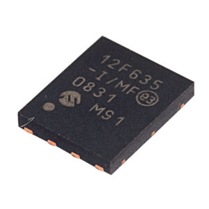
La restauration du code flash du microprocesseur PIC12F635 verrouillé est un processus permettant de lire le programme intégré à partir du MCU sécurisé PIC12F635, puis de copier le micrologiciel sur le nouveau microcontrôleur PIC12F635
The Two-Speed Start-up feature helps to minimize the latency period from oscillator start-up to code execution by allowing the microcontroller to use the INTRC oscillator as a clock source until the primary clock source is available. It is enabled by setting the IESO bit in Configuration Register 1H (CONFIG1H<7>).
Two-Speed Start-up is available only if the primary oscil- lator mode is LP, XT, HS or HSPLL (crystal-based modes). Other sources do not require an OST start-up delay to read microcontroller pic12f509 flash heximal; for these, Two-Speed Start-up is disabled.
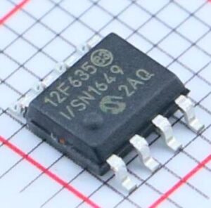
Восстановление заблокированного кода флэш-памяти микропроцессора PIC12F635 — это процесс считывания встроенной программы из защищенного микроконтроллера PIC12F635 с последующим копированием прошивки на новый микроконтроллер PIC12F635.
When enabled, Resets and wake-ups from Sleep mode cause the device to configure itself to run from the internal oscillator block as the clock source, following the time-out of the Power-up Timer after a Power-on Reset is enabled. This allows almost immediate code execution while the primary oscillator starts and the OST is running to clone microchip pic12f510 microcontroller flash program. Once the OST times out, the device automatically switches to PRI_RUN mode.
 Unlock Microchip PIC12F615 MCU Flash Memory
Unlock Microchip PIC12F615 MCU Flash Memory and extract embedded firmware from PIC12F615 microcontroller original IC MCU PIC12F615 chip protection can be broken off;
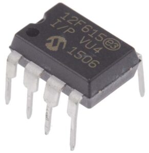
Entsperren Sie den Microchip PIC12F615 MCU-Flash-Speicher und extrahieren Sie die eingebettete Firmware aus dem PIC12F615-Mikrocontroller. Der ursprüngliche IC-MCU-PIC12F615-Chipschutz kann abgebrochen werden.
For PIC12F615 devices, the WDT is driven by the INTRC source. When the WDT is enabled, the clock source is also enabled. The nominal WDT period is 4 ms and has the same stability as the INTRC oscillator to break microchip pic12f1571 mcu protection.
The 4 ms period of the WDT is multiplied by a 16-bit postscaler. Any output of the WDT postscaler is selected by a multiplexer, controlled by bits in Configuration Register 2H. Available periods range from 4 ms to
131.072 seconds (2.18 minutes). The WDT and postscaler are cleared when any of the following events occur: execute a SLEEP or CLRWDT instruction by breaking microchip pic12f508 processor flash memory, the IRCF bits (OSCCON<6:4>) are changed or a clock failure has occurred.
Entsperren Sie den Microchip PIC12F615 MCU-Flash-Speicher und extrahieren Sie die eingebettete Firmware aus dem PIC12F615-Mikrocontroller. Der ursprüngliche IC-MCU-PIC12F615-Chipschutz kann abgebrochen werden.
Adjustments to the internal oscillator clock period using the OSCTUNE register also affect the period of the WDT by the same factor. For example, if the INTRC period is increased by 3%, then the WDT period is increased by 3%.
Register 19-14 shows the WDTCON register. This is a readable and writable register, which contains a control bit that allows software to override the WDT enable Configuration bit, only if the Configuration bit has disabled the WDT.
 Locked Microchip PIC12F615 Processor Data Restoration
Locked Microchip PIC12F615 Processor Data Restoration is a process to copy embedded firmware from original MCU PIC12F615 flash memory after break off the tamper resistance system of PIC12F615 locked microcontroller;

A Restauração de Dados do Processador PIC12F615 de Microchip Bloqueado é um processo para copiar o firmware incorporado da memória flash MCU PIC12F615 original após interromper o sistema de resistência à violação do microcontrolador bloqueado PIC12F615;
The Configuration bits can be programmed (read as ‘0’), or left unprogrammed (read as ‘1’), to select vari- ous device configurations. These bits are mapped starting at program memory location 300000h.
The user will note that address 300000h is beyond the user program memory space. In fact, it belongs to the configuration memory space (300000h-3FFFFFh), which can only be accessed using table reads and table writes.
Programming the Configuration registers is done in a manner similar to programming the Flash memory. The EECON1 register WR bit starts a self-timed write to the Configuration register. In normal operation mode, a TBLWT instruction, with the TBLPTR pointing to the Configuration register, sets up the address and the data for the Configuration register write.

Il ripristino dei dati del processore PIC12F615 del microchip bloccato è un processo per copiare il firmware incorporato dalla memoria flash originale dell’MCU PIC12F615 dopo aver interrotto il sistema di resistenza alle manomissioni del microcontrollore bloccato PIC12F615;
Setting the WR bit starts a long write to the Configuration register. The Configuration registers are written a byte at a time. To write or erase a configuration cell by breaking pic12f635 locked microprocessor fuse bit, a TBLWT instruction can write a ‘1’ or a ‘0’ into the cell. For additional details on Flash programming, refer to Section 6.5 “Writing to Flash Program Memory”.
bit 7 IESO: Internal External Switchover bit
1 = Internal External Switchover mode enabled
0 = Internal External Switchover mode disabled bit 6 FSCM: Fail-Safe Clock Monitor Enable bit
1 = Fail-Safe Clock Monitor enabled
0 = Fail-Safe Clock Monitor disabled
bit 5-4 Unimplemented: Read as ‘0’
bit 3-0 FOSC<3:0>: Oscillator Selection bits
11xx = External RC oscillator, CLKO function on RA6
1001 = Internal RC oscillator, CLKO function on RA6 and port function on RA7 1000 = Internal RC oscillator, port function on RA6 and port function on RA7 0111 = External RC oscillator, port function on RA6 when breaking pic12f609 locked mcu flash memory;
0110 = HS oscillator, PLL enabled (clock frequency = 4 x FOSC1)
0101 = EC oscillator, port function on RA6 0100 = EC oscillator, CLKO function on RA6 0010 = HS oscillator
0001 = XT oscillator
0000 = LP oscillator
 Recover PIC12F612 Secured Microchip MCU Flash Heximal
recover PIC12F612 Secured Microchip MCU flash heximal after attack PIC12F612 locked microcontroller security fuse bit, then dump embedded firmware from encrypted microprocessor PIC12F612 from its flash and eeprom memory;
recupere PIC12F612 Secured Microchip MCU flash heximal después del ataque PIC12F612 bloqueó el bit de fusible de seguridad del microcontrolador, luego descargue el firmware integrado del microprocesador cifrado PIC12F612 de su memoria flash y eeprom;
A complete discussion of device Resets and interrupts is available in previous sections of this data sheet.
In addition to their Power-up and Oscillator Start-up Timers provided for Resets, PIC12F612 devices have a Watchdog Timer, which is either permanently enabled via the Configuration bits, or software controlled (if configured as disabled) when break pic12f629 microcontroller flash memory.
The inclusion of an internal RC oscillator also provides the additional benefits of a Fail-Safe Clock Monitor (FSCM) and Two-Speed Start-up. FSCM provides for background monitoring of the peripheral clock and automatic switchover in the event of its failure.
recuperați PIC12F612 Secured Microcip MCU flash heximal după atac PIC12F612 blocat bitul siguranței de securitate al microcontrolerului, apoi descărcați firmware-ul încorporat de la microprocesorul criptat PIC12F612 din memoria flash și eeprom;
Two- Speed Start-up enables code to be executed almost immediately on start-up, while the primary clock source completes its start-up delays to copy pic12f675 secured microcontroller flash memory. All of these features are enabled and configured by setting the appropriate Configuration register bits.
 Microchip PIC12F609 Processor Flash Binary Duplication
Microchip PIC12F609 Processor Flash Binary Duplication can help engineer to unlock microcontroller pic12f609 heximal, and copy embedded firmware to new microprocessor pic12f609;
La duplicación binaria flash del procesador PIC12F609 de Microchip puede ayudar al ingeniero a desbloquear el microcontrolador pic12f609 heximal y copiar el firmware incorporado al nuevo microprocesador pic12f609
Depending on the power source for the device voltage, the voltage normally decreases relatively slowly. This means that the LVD module does not need to be constantly operating when breaking off pic12f615 mcu software. To decrease the current require- ments, the LVD circuitry only needs to be enabled for short periods, where the voltage is checked. After doing the check, the LVD module may be disabled.
Each time that the LVD module is enabled, the circuitry requires some time to stabilize. After the circuitry has stabilized, all status flags may be cleared in the process of breaking pic12f609 ic chip flash memory. The module will then indicate the proper state of the system.
Ataque el microcontrolador PIC12F609 bloqueado y deshabilite el bit de fusible de seguridad, restaure el archivo heximal en la memoria flash MCU PIC12F609;
The following steps are needed to set up the LVD module:
- Write the value to the LVDL3:LVDL0 bits (LVDCON register), which selects the desired LVD trip
- Ensure that LVD interrupts are disabled (the LVDIE bit is cleared or the GIE bit is cleared).
- Enable the LVD module (set the LVDEN bit in the LVDCON register).
- Wait for the LVD module to stabilize (the IRVST bit to become set).
- Clear the LVD interrupt flag, which may have falsely become set, until the LVD module has stabilized (clear the LVDIF bit).
- Enable the LVD interrupt (set the LVDIE and the GIE bits).
 Replicate PIC12F519 Microprocessor Flash Program
Replicate PIC12F519 Microprocessor Flash Program can help engineer to unlock ic chip secured pic12f519 binary from its flash memory, to readout microchip locked pic12f519 source code;
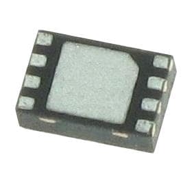
Çoğaltma PIC12F519 Mikroişlemci Flash Programı, mühendisin ic çip korumalı pic12f519 ikili dosyasını flash belleğinden açmasına, mikroçip kilitli pic12f519 kaynak kodunu okumasına yardımcı olabilir
The LVD module has an additional feature that allows the user to supply the trip voltage to the module from an external source. This mode is enabled when bits, LVDL3:LVDL0, are set to ‘1111’. In this state, the com- parator input is multiplexed from the external input pin when breaking microcontroller pic12f629 flash, LVDIN (Figure 18-3). This gives users flexibility, because it allows them to configure the Low-Voltage Detect interrupt to occur at any voltage in the valid operating range.
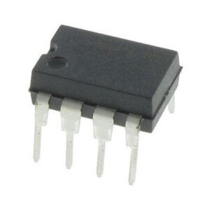
Kilitli mikrodenetleyici PIC12F519’un kurcalamaya karşı direnç sistemini kırma ve PIC12F519 MCU flash bellekten onaltılık dosyayı kurtarma;
bit 7-6 Unimplemented: Read as ‘0’
bit 5 IRVST: Internal Reference Voltage Stable Flag bit
1 = Indicates that the Low-Voltage Detect logic will generate the interrupt flag at the specified voltage range
0 = Indicates that the Low-Voltage Detect logic will not generate the interrupt flag at the specified volt- age range and the LVD interrupt should not be enabled by breaking dspic30f4011 mcu flash memory;
bit 4 LVDEN: Low-Voltage Detect Power Enable bit
1 = Enables LVD, powers up LVD circuit
0 = Disables LVD, powers down LVD circuit
bit 3-0 LVDL<3:0>: Low-Voltage Detection Limit bits(1)
1111 = External analog input is used (input comes from the LVDIN pin)
1110 = 4.04V-5.15V
1101 = 3.76V-4.79V
1100 = 3.58V-4.56V
1011 = 3.41V-4.34V
1010 = 3.23V-4.11V
1001 = 3.14V-4.00V
1000 = 2.96V-3.77V
0111 = 2.70V-3.43V
0110 = 2.53V-3.21V
0101 = 2.43V-3.10V
0100 = 2.25V-2.86V
0011 = 2.16V-2.75V
0010 = 1.99V-2.53V
0001 = Reserved
0000 = Reserved
Note 1: LVDL<3:0> modes, which result in a trip point below the valid operating voltage of the device, are not tested.
 Clone Microchip PIC12F510 Microcontroller Flash Program
Clone Microchip PIC12F510 Microcontroller Flash Program and rewrite the heximal file to new MCU PIC12F510, the lock bit of PIC12F510 microprocessor will be unlocked and original firmware can be copied from pic12f510 MCU;
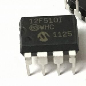
Klonuokite mikroschemą PIC12F510 mikrovaldiklio Flash programa ir perrašykite šešioliktainį failą į naują MCU PIC12F510, PIC12F510 mikroprocesoriaus blokavimo bitas bus atrakintas ir originali programinė įranga gali būti nukopijuota iš pic12f510 MCU.
An A/D conversion can be started by the “special event trigger” of the CCP1 module. This requires that the CCP1M3:CCP1M0 bits (CCP1CON<3:0>) be programmed as ‘1011’ and that the A/D module is enabled (ADON bit is set). When the trigger occurs, the GO/ DONE bit will be set, starting the A/D acquisition and conversion and the Timer1 (or Timer3) counter will be reset to zero.
Timer1 (or Timer3) is reset to auto-matically repeat the A/D acquisition period with minimal software overhead (moving ADRESH/ADRESL to the desired location). The appropriate analog input channel must be selected and the minimum acquisition period is either timed by the user to unlock pic12f510 mcu fuse bit, or an appropriate TACQ time selected before the “special event trigger” sets the GO/DONE bit (starts a conversion).
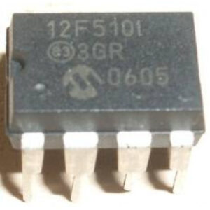
Klon Mikrochip PIC12F510 Mikrokontroller Flash Programm a schreift d’heximal Datei op den neie MCU PIC12F510, de Sperrbit vum PIC12F510 Mikroprozessor gëtt opgehuewen an d’originell Firmware kann vum pic12f510 MCU kopéiert ginn
If the A/D module is not enabled (ADON is cleared), the “special event trigger” will be ignored by the A/D module, but will still reset the Timer1 (or Timer3) counter.
x = unknown, u = unchanged, q = depends on CONFIG1H<3:0>, – = unimplemented, read as ‘0’.
Shaded cells are not used for A/D conversion.
Note 1: RA5 port bit is available only as an input pin when the MCLRE bit in the Configuration register is ‘0’.
2: RA6 and TRISA6 are available only when the primary oscillator mode selection offers RA6 as a port pin; otherwise, RA6 always reads ‘0’, TRISA6 always reads ‘1’ and writes to both are ignored (see CONFIG1H<3:0>).
3: RA7 and TRISA7 are available only when the internal RC oscillator is configured as the primary oscillator in CON- FIG1H<3:0> by cracking microcontroller pic12f510 flash memory program; otherwise, RA7 always reads ‘0’, TRISA7 always reads ‘1’ and writes to both are ignored.
 Read Microcontroller PIC12F509 Flash Heximal
Read Microcontroller PIC12F509 Flash Heximal needs to crack pic mcu pic12f509 security fuse bit, extract mcu pic12f509 embedded firmware from its flash memory;
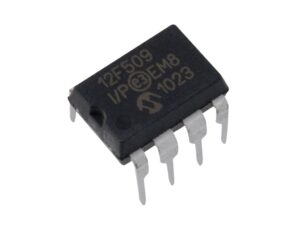
Leggi il microcontrollore PIC12F509 Flash Heximal ha bisogno di rompere il bit del fusibile di sicurezza pic mcu pic12f509, estrarre il firmware incorporato mcu pic12f509 dalla sua memoria flash;
Figure 17-3 shows the operation of the A/D converter after the GO bit has been set and the ACQT2:ACQT0 bits are cleared. A conversion is started after the following instruction to allow entry into Low-Power Sleep mode before the conversion begins.
Figure 17-4 shows the operation of the A/D converter after the GO bit has been set and the ACQT2:ACQT0 bits are set to ‘010’ and selecting a 4 TAD acquisition time before the conversion starts.
Clearing the GO/DONE bit during a conversion will abort the current conversion. The A/D Result register pair will NOT be updated with the partially completed A/ D conversion sample when break off pic12f509 eeprom and flash memory fuse bit. This means the ADRESH:ADRESL registers will continue to contain the value of the last completed conversion (or the last value written to the ADRESH:ADRESL registers).
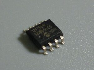
Copia il programma di memoria flash del processore PIC12F509 del microchip e riscrivi il file esadecimale o binario sul nuovo microcontrollore PIC12F509 per la clonazione dell’MCU
After the A/D conversion is completed or aborted, a 2 TAD wait is required before the next acquisition can be started. After this wait, acquisition on the selected channel is automatically started.
 Microchip PIC12F508 Processor Flash Memory Breaking
Microchip PIC12F508 Processor Flash Memory Breaking will disable the protection over the flash memory, original embedded firmware will be read through programmer;
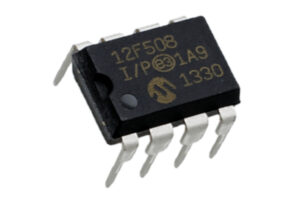
Przerwanie pamięci flash procesora Microchip PIC12F508 spowoduje wyłączenie ochrony pamięci flash, oryginalne wbudowane oprogramowanie sprzętowe zostanie odczytane przez programator
If the low-power mode clock frequency is less than 1 MHz, the A/D RC clock source should be selected. Operation in the Low-Power Sleep mode requires the A/ D RC clock to be selected. If bits, ACQT2:ACQT0, are set to ‘000’ and a conversion is started, the conversion will be delayed one instruction cycle to allow execution of the SLEEP instruction and entry to Low-Power Sleep mode by recovering pic12f508 mcu source code. The IDLEN and SCS bits in the OSCCON register must have already been cleared prior to starting the conversion.
The ADCON1, TRISA and TRISB registers all configure the A/D port pins. The port pins needed as analog inputs must have their corresponding TRIS bits set (input). If the TRIS bit is cleared (output), the digital output level (VOH or VOL) will be converted. The A/D operation is independent of the state of the CHS2:CHS0 bits and the TRIS bits.
Mikrokontroler Microchip PIC12F508 łamie i wyodrębnia plik szesnastkowy z jego pamięci flash i pamięci eeprom,
When reading the Port register, all pins configured as analog input channels will read as cleared (a low level). Pins con- figured as digital inputs will convert an analog input. Analog levels on a digitally configured input will be accurately converted to decrypt locked chip pic12f508 firmware from its flash memory.
Analog levels on any pin defined as a digital input may cause the digital input buffer to consume current out of the device’s specification limits.
 Reverse DSP MCU TMS320F28062PZT Flash Firmware
Reverse DSP MCU TMS320F28062PZT Flash Firmware is a process to unlock dsp microcontroller tms320f28062 encryption over its flash memory, and then the binary code will be readout from microprocessor tms320f28062pzt flash memory;
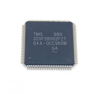
Reverse DSP MCU TMS320F28062PZT Flash Firmware is a process to unlock dsp microcontroller tms320f28062 encryption over its flash memory, and then the binary code will be readout from microprocessor tms320f28062pzt flash memory
The peripheral – I/O multiplexing implemented in the device prevents all available peripherals from being used at the same time. This is because more than one peripheral function may share an I/O pin. It is, however, possible to turn on the clocks to all the peripherals at the same time, although such a configuration is not useful. If this is done, the current drawn by the device will be more than the numbers specified in the current consumption tables.
The 2803x devices incorporate a method to reduce the device current consumption. Because each peripheral unit has an individual clock-enable bit, significant reduction in current consumption can be achieved by turning off the clock to any peripheral module that is not used in a given application. Furthermore, any one of the three low-power modes could be taken advantage of to reduce the current consumption even further. Table 7-1 indicates the typical reduction in current consumption achieved by turning off the clocks.
All peripheral clocks (except CPU Timer clock) are disabled upon reset. Writing to/reading from peripheral registers is possible only after the peripheral clocks are turned; This number represents the current drawn by the digital portion of the ADC module. Turning off the clock to the ADC module results in the elimination of the current drawn by the analog portion of the ADC (IDDA) as well.
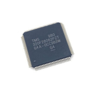
Обратное прошивка DSP MCU TMS320F28062PZT Flash — это процесс разблокировки шифрования микроконтроллера tms320f28062 dsp через его флэш-память, после чего двоичный код будет считан из флэш-памяти микропроцессора tms320f28062pzt.
For peripherals with multiple instances, the current quoted is per For example, the 2 mA value quoted for ePWM is for one ePWM module.The baseline IDD current (current when the core is executing a dummy loop with no peripherals enabled) is 40 mA, typical. To arrive at the IDD current for a given application, the current-drawn by the peripherals (enabled by that application) must be added to the baseline IDD current.