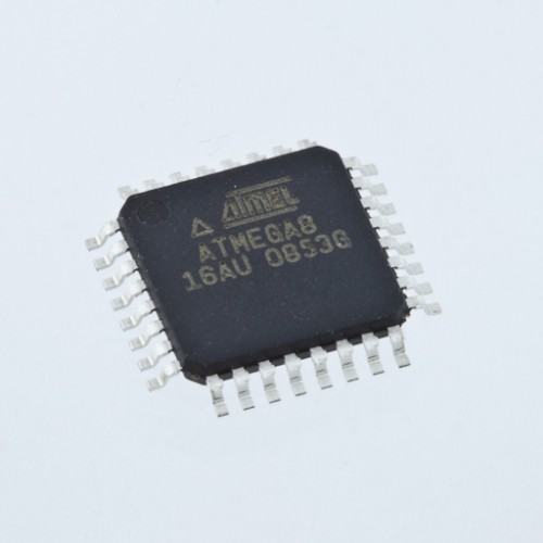
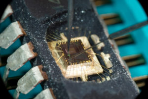
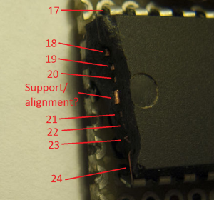
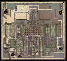
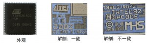
 Attack Chip ATmega8A Binary
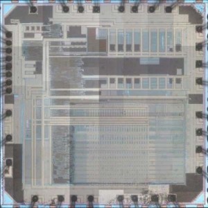
Attack Chip ATmega8A secured system, unlock microcontroller ATmega8A flash and eeprom memory, extract binary from both of the memories in the format of heximal which can be used for microcontroller copying
Attack Chip ATmega8A secured system, unlock microcontroller ATmega8A flash and eeprom memory, extract binary from both of the memories in the format of heximal which can be used for microcontroller copying;
Features
· High-performance, Low-power AVR® 8-bit Microcontroller
· Advanced RISC Architecture
– 130 Powerful Instructions – Most Single-clock Cycle Execution
– 32 x 8 General Purpose Working Registers when Chip PIC16F84A binary copying
– Fully Static Operation
– Up to 16 MIPS Throughput at 16 MHz
– On-chip 2-cycle Multiplier
High Endurance Non-volatile Memory segments
– 8K Bytes of In-System Self-programmable Flash program memory
– 512 Bytes EEPROM
– 1K Byte Internal SRAM
– Write/Erase Cycles: 10,000 Flash/100,000 EEPROM
– Data retention: 20 years at 85°C/100 years at 25°C(1)
– Optional Boot Code Section with Independent Lock Bits
· In-System Programming by On-chip Boot Program
· True Read-While-Write Operation
crack ATmega8A microprocessor and extract heximal code from flash memory
8-bit with 8K Bytes In-System Programmable
– Programming Lock for Software Security
Peripheral Features
– Two 8-bit Timer/Counters with Separate Prescaler, one Compare Mode
– One 16-bit Timer/Counter with Separate Prescaler, Compare Mode, and Capture Mode
– Real Time Counter with Separate Oscillator after IC C8051F530 Firmware attacking
– Three PWM Channels
– 8-channel ADC in TQFP and QFN/MLF package
· Eight Channels 10-bit Accuracy
– 6-channel ADC in PDIP package
· Six Channels 10-bit Accuracy
– Byte-oriented Two-wire Serial Interface
– Programmable Serial USART
– Master/Slave SPI Serial Interface
– Programmable Watchdog Timer with Separate On-chip Oscillator
– On-chip Analog Comparator
Special Microcontroller Features
– Power-on Reset and Programmable Brown-out Detection
– Internal Calibrated RC Oscillator
– External and Internal Interrupt Sources
– Five Sleep Modes: Idle, ADC Noise Reduction, Power-save, Power-down, and Standby
I/O and Packages
– 23 Programmable I/O Lines
– 28-lead PDIP, 32-lead TQFP, and 32-pad QFN/MLF
Operating Voltages
– 2.7 – 5.5V for ATmega8A
Speed Grades
– 0 – 16 MHz for ATmega8A
Power Consumption at 4 Mhz, 3V, 25°C
Flash ATmega8A
– Active: 3.6 mA
– Idle Mode: 1.0 mA
– Power-down Mode: 0.5 µA
Attack Microcontroller PIC16C63A Heximal
Attack Microcontroller PIC16C63A protective memory and readout heximal of MCU PIC16C63A flash memory, microprocessor PIC16C63A unlocking process will normally start from chip surface decapsulation;
Attack Microcontroller PIC16C63A protective memory and readout heximal of MCU PIC16C63A flash memory, microprocessor PIC16C63A unlocking process will normally start from chip surface decapsulation
Devices included in this data sheet:
PIC16C7X Peripheral Features:
· Timer0: 8-bit timer/counter with 8-bit prescaler
· Timer1: 16-bit timer/counter with prescaler can be incremented during SLEEP via external
PIC16CXX Microcontroller Core Features:
· High performance RISC CPU
· Only 35 single word instructions to learn
· All single cycle instructions except for program branches which are two cycle
· Operating speed: DC – 20 MHz clock input
DC – 200 ns instruction cycle
· 4 K x 14 words of Program Memory,
192 x 8 bytes of Data Memory (RAM)
· Interrupt capability
· Eight-level deep hardware stack
· Direct, indirect and relative addressing modes
· Power-on Reset (POR)
· Power-up Timer (PWRT) and Oscillator Start-up Timer (OST)
· Watchdog Timer (WDT) with its own on-chip RC oscillator for reliable operation
· Programmable code protection
· Power-saving SLEEP mode crystal/clock
· Timer2: 8-bit timer/counter with 8-bit period register, prescaler and postscaler
· Capture, Compare, PWM modules
– Capture is 16-bit, max. resolution is 200 ns
– Compare is 16-bit, max. resolution is 200 ns
– PWM max. resolution is 10-bit
· 8-bit multichannel Analog-to-Digital converter
· Synchronous Serial Port (SSP) with SPITM and I2CTM
· Universal Synchronous Asynchronous Receiver Transmitter (USART/SCI)
· Parallel Slave Port (PSP), 8-bits wide with external RD, WR and CS controls when Attack Microcontroller
· Brown-out detection circuitry for Brown-out Reset (BOR) Pin Diagram: PDIP, Windowed CERDIP
· Selectable oscillator options
· Low power, high speed CMOS EPROM technology
· Wide operating voltage range: 2.5V to 5.5V
· High Sink/Source Current 25/25 mA
· Commercial, Industrial and Automotive temperature ranges
· Low power consumption:
– < 5 mA @ 5V, 4 MHz
– 23 mA typical @ 3V, 32 kHz
– < 1.2 mA typical standby current
Attack MCU PIC16CE625 Program
Attack MCU PIC16CE625 locked memory and extract program from Microcontroller PIC16CE625 flash memory, disable the security fuse bit after crack Microprocessor PIC16CE625 so the microprobes will be able to get access to the internal memory
Attack MCU PIC16CE625 locked memory and extract program from Microcontroller PIC16CE625 flash memory, disable the security fuse bit after crack Microprocessor PIC16CE625 so the microprobes will be able to get access to the internal memory;
Interrupt capability 16 special function hardware registers
8-level deep hardware stack
Direct, Indirect and Relative addressing modes
Peripheral Features:
· 13 I/O pins with individual direction control
· High current sink/source for direct LED drive
· Analog comparator module with:
– Two analog comparators
– Programmable on-chip voltage reference (VREF) module
– Programmable input multiplexing from device inputs and internal voltage reference
– Comparator outputs can be output signals
· Timer0: 8-bit timer/counter with 8-bit programmable prescaler
Special Microcontroller Features:
· In-Circuit Serial Programming (ICSP™) (via two pins)
· Power-on Reset (POR)
· Power-up Timer (PWRT) and Oscillator Start-up Timer (OST)
· Brown-out Reset
· Watchdog Timer (WDT) with its own on-chip RC oscillator for reliable operation
Special Microcontroller Features (cont’d)
· 1,000,000 erase/write cycle EEPROM data memory
· EEPROM data retention > 40 years
· Programmable code protection
· Power saving SLEEP mode
· Selectable oscillator options
· Four user programmable ID locations
CMOS Technology:
· Low-power, high-speed CMOS EPROM/EEPROM technology
· Fully static design
· Wide operating voltage range – 2.5V to 5.5V
· Commercial, industrial and extended temperature range
· Low power consumption
– < 2.0 mA @ 5.0V, 4.0 MHz
– 15 mA typical @ 3.0V, 32 kHz
– < 1.0 mA typical standby current @ 3.0V
Break Microcontroller PIC18F8722 Flash

Break Microcontroller PIC18F8722 Flash memory tamper resistance system off, and then extract IC PIC18F8722 code from flash memory, the content can be reprogrammed to new unit for Microcontroller PIC18F8722 cloning
Break Microcontroller PIC18F8722 Flash memory tamper resistance system off, and then extract IC PIC18F8722 code from flash memory, the content can be reprogrammed to new unit for Microcontroller PIC18F8722 cloning;
Power-Managed Modes:
Peripheral Highlights (Continued):
Run: CPU on, peripherals on
Idle: CPU off, peripherals on
Sleep: CPU off, peripherals off
Idle mode currents down to 15 µA typical
Sleep current down to 0.2 µA typical
Timer1 Oscillator: 1.8 µA, 32 kHz, 2V
Watchdog Timer: 2.1 µA
Two-Speed Oscillator Start-up
· Three Enhanced Capture/Compare/PWM (ECCP) modules
– One, two or four PWM outputs
– Selectable polarity
– Programmable dead-time
– Auto-Shutdown and Auto-Restart
· Two Master Synchronous Serial Port (MSSP) modules supporting 2/3/4-wire SPI™ (all 4 modes) and I2C™ Master and Slave modes
Flexible Oscillator Structure:
· Four Crystal modes, up to 25 MHz
· 4X Phase Lock Loop (PLL) (available for crystal and internal oscillators)
· Two External RC modes, up to 4 MHz
· Two External Clock modes, up to 40 MHz
· Internal oscillator block:
– 8 user selectable frequencies, from 31 kHz to 8 MHz
– Provides a complete range of clock speeds from 31 kHz to 32 MHz when used with PLL
– User tunable to compensate for frequency drift
· Secondary oscillator using Timer1 @ 32 kHz
· Fail-Safe Clock Monitor:
– Allows for safe shutdown if peripheral clock stops External Memory Interface (PIC18F8627/8722 only):
· Address capability of up to 2 Mbytes
· 8-bit or 16-bit interface
Peripheral Highlights:
· Two Enhanced Addressable USART modules
– Supports RS-485, RS-232 and LIN 1.2
– RS-232 operation using internal oscillator block (no external crystal required)
– Auto-wake-up on Start bit
– Auto-baud detect
· 10-bit, up to 16-channel Analog-to-Digital Converter module (A/D)
– Auto-acquisition capability
– Conversion available during Sleep
· Dual analog comparators with input multiplexing
Special Microcontroller Features:
· C compiler optimized architecture:
– Optional extended instruction set designed to optimize re-entrant code
· 100,000 erase/write cycle Enhanced Flash program memory typical
· 1,000,000 erase/write cycle Data EEPROM memory typical
· Flash/Data EEPROM Retention: 100 years typical
· Self-programmable under software control
High current sink/source 25 mA/25 mA
Four programmable external interrupts
Four input change interrupts
Two Capture/Compare/PWM (CCP) modules
· Priority levels for interrupts
· 8 X 8 Single Cycle Hardware Multiplier
· Extended Watchdog Timer (WDT):
– Programmable period from 4 ms to 131s
· Single-supply In-Circuit Serial Programming™ (ICSP™) via two pins
· In-Circuit Debug (ICD) via two pins
· Wide operating voltage range: 2.0V to 5.5V
Attack IC C8051F530 Firmware
Attack IC C8051F530 protective system and remove its security fuse bit, extract firmware out from MCU C8051F530 flash memory, copy heximal to blank Microcontroller C8051F530 which will provide the same functions
Attack IC C8051F530 protective system and remove its security fuse bit, extract firmware out from MCU C8051F530 flash memory, copy heximal to blank Microcontroller C8051F530 which will provide the same functions;
Analog Peripherals
– 12-Bit ADC
· ±1 LSB INL (C8051F52x/C8051F53x); no missing codes
· Programmable throughput up to 200 ksps
· Up to 6/16 external inputs
· Data dependent windowed interrupt generator
· Built-in temperature sensor
– Comparator
· Programmable hysteresis and response time
· Configurable as wake-up or reset source
· Low current
– POR/Brownout Detector
– Voltage Reference—1.5 to 2.2 V (programmable)
On-Chip Debug
– On-chip debug circuitry facilitates full-speed, non-intrusive in-system debug (No emulator required)
– Provides breakpoints, single stepping
– Inspect/modify memory and registers
– Complete development kit
Supply Voltage 2.7 to 5.25 V
– Built-in LDO regulator
High Speed 8051 µC Core
– Pipelined instruction architecture; executes 70% of instructions in 1 or 2 system clocks
– Up to 25 MIPS throughput with 25 MHz system clock
Memory
– 8/4/2 kB Flash; In-system byte programmable in 512 byte sectors
– 256 bytes internal data RAM
Digital Peripherals
– 16/6 port I/O; push-pull or open-drain, 5 V tolerant
– Hardware SPI™, and UART serial port
– Hardware LIN (both master and slave, compatible with V1.3 and V2.0)
– Three general purpose 16-bit counter/timers
– Programmable 16-bit counter/timer array with three capture/compare modules, WDT
Clock Sources
– Internal oscillators: 24.5 MHz ±0.5% accuracy supports UART and LIN-Master operation
– External oscillator: Crystal, RC, C, or Clock (1 or 2 pin modes)
– Can switch between clock sources on-the-fly
Packages:
– 10-Pin QFN (3 x 3 mm)
– 20-pin QFN (4 x 4 mm)
– 20-pin TSSOP
Temperature Range: –40 to +125 °C
Break Chip PIC16F917 Heximal
Break Chip PIC16F917 tamper resistance system and readout MCU PIC16F917 heximal from flash memory and eeprom memory, the program and data will be exactly the same as master original PIC16F917 microprocessor
Break Chip PIC16F917 tamper resistance system and readout MCU PIC16F917 heximal from flash memory and eeprom memory, the program and data will be exactly the same as master original PIC16F917 microprocessor;
High-Performance RISC CPU:
· Only 35 instructions to learn:
– All single-cycle instructions except branches
· Operating speed:
– DC – 20 MHz oscillator/clock input
– DC – 200 ns instruction cycle
· Program Memory Read (PMR) capability
· Interrupt capability
· 8-level deep hardware stack
· Direct, Indirect and Relative Addressing modes
Special Microcontroller Features:
· Precision Internal Oscillator:
– Factory calibrated to ±1%
– Software selectable frequency range of 8 MHz to 32 kHz
– Software tunable
– Two-Speed Start-up mode
– Crystal fail detect for critical applications
– Clock mode switching during operation for power savings
· Power-saving Sleep mode
· Wide operating voltage range (2.0V-5.5V)
· Industrial and Extended temperature range
· Power-on Reset (POR)
· Power-up Timer (PWRT) and Oscillator Start-up Timer (OST)
· Brown-out Reset (BOR) with software control option
· Enhanced Low-Current Watchdog Timer (WDT) with on-chip oscillator (software selectable nominal 268 seconds with full prescaler) with software enable
· Multiplexed Master Clear with pull-up/input pin
· Programmable code protection
· High-Endurance Flash/EEPROM cell:
– 100,000 write Flash endurance
– 1,000,000 write EEPROM endurance
– Flash/Data EEPROM retention: > 40 years
Low-Power Features:
· Standby Current:
– <100 nA @ 2.0V, typical
· Operating Current:
– 8.5 ìA @ 32 kHz, 2.0V, typical
– 100 ìA @ 1 MHz, 2.0V, typical
· Watchdog Timer Current:
– 1 ìA @ 2.0V, typical
Peripheral Features:
· Liquid Crystal Display module:
– Up to 60 pixel drive capability on 28-pin devices
– Up to 96 pixel drive capability on 40-pin devices
– Four commons
· Up to 35 I/O pins and 1 input-only pin:
– High-current source/sink for direct LED drive
– Interrupt-on-pin change
– Individually programmable weak pull-ups
· In-Circuit Serial Programming™ (ICSP™) via two pins
· Analog comparator module with:
– Two analog comparators
– Programmable on-chip voltage reference (CVREF) module (% of VDD)
– Comparator inputs and outputs externally accessible
· A/D Converter:
– 10-bit resolution and up to 8 channels
· Timer0: 8-bit timer/counter with 8-bit programmable prescaler
· Enhanced Timer1:
– 16-bit timer/counter with prescaler
– External Gate Input mode
– Option to use OSC1 and OSC2 as Timer1 oscillator if INTOSCIO or LP mode is selected
· Timer2: 8-bit timer/counter with 8-bit period register, prescaler and postscaler
· Addressable Universal Synchronous
Asynchronous Receiver Transmitter (AUSART)
· Up to 2 Capture, Compare, PWM modules:
– 16-bit Capture, max. resolution 12.5 ns
– 16-bit Compare, max. resolution 200 ns
– 10-bit PWM, max. frequency 20 kHz
· Synchronous Serial Port (SSP) with I2C™
Copy Chip PIC16F870 Program
Copy Chip PIC16F870 Program and data out from microcontroller PIC16F870 flash memory and eeprom memory, reset the status of MCU PIC16F870 from locked to unlocked one after disable its security fuse bit by MCU crack technique
Copy Chip PIC16F870 Program and data out from microcontroller PIC16F870 flash memory and eeprom memory, reset the status of MCU PIC16F870 from locked to unlocked one after disable its security fuse bit by MCU crack technique;
Microcontroller Core Features:
· High performance RISC CPU
· Only 35 single word instructions to learn
· All single cycle instructions except for program branches which are two-cycle
· Operating speed: DC – 20 MHz clock input DC – 200 ns instruction cycle
· 2K x 14 words of FLASH Program Memory
128 x 8 bytes of Data Memory (RAM) 64 x 8 bytes of EEPROM Data Memory
· Pinout compatible to the PIC16CXXX 28 and 40-pin devices
· Interrupt capability (up to 11 sources)
· Eight level deep hardware stack
· Direct, Indirect and Relative Addressing modes;
· Power-on Reset (POR)
· Power-up Timer (PWRT) and
Oscillator Start-up Timer (OST)
· Watchdog Timer (WDT) with its own on-chip RC oscillator for reliable operation when MCU STM32F107RCT6 code recovery
· Programmable code protection
· Power saving SLEEP mode
· Selectable oscillator options
· Low power, high speed CMOS FLASH/EEPROM technology
· Fully static design
· In-Circuit Serial Programmingä (ICSPä) via two pins
· Single 5V In-Circuit Serial Programming capability
· In-Circuit Debugging via two pins
· Processor read/write access to program memory
· Wide operating voltage range: 2.0V to 5.5V
· High Sink/Source Current: 25 mA
· Commercial and Industrial temperature ranges
· Low power consumption:
– < 1.6 mA typical @ 5V, 4 MHz
– 20 mA typical @ 3V, 32 kHz
– < 1 mA typical standby current
Peripheral Features:
· Timer0: 8-bit timer/counter with 8-bit prescaler
· Timer1: 16-bit timer/counter with prescaler, can be incremented during SLEEP via external crystal/clock
· Timer2: 8-bit timer/counter with 8-bit period register, prescaler and postscaler
· One Capture, Compare, PWM module
– Capture is 16-bit, max. resolution is 12.5 ns
– Compare is 16-bit, max. resolution is 200 ns
– PWM max. resolution is 10-bit
· 10-bit multi-channel Analog-to-Digital converter only
· Universal Synchronous Asynchronous Receiver
Transmitter (USART/SCI) with 9-bit address detection
· Parallel Slave Port (PSP) 8-bits wide, with external RD, WR and CS controls (40/44-pin only)
· Brown-out detection circuitry for Brown-out Reset (BOR)
Copy IC PIC16F84A Binary
Copy IC PIC16F84A Binary out from microcontroller PIC16F84A flash memory, and reprogramme the firmware into blank MCU PIC16F84A which will provide the same functions as original version
Copy IC PIC16F84A Binary out from microcontroller PIC16F84A flash memory, and reprogramme the firmware into blank MCU PIC16F84A which will provide the same functions as original version, the status of master original MICROPROCESSOR PIC16F84A can be unlocked;
The PIC16F8X is a group in the PIC16CXX family of low-cost, high-performance, CMOS, fully-static, 8-bit microcontrollers. This group contains the following devices:
· PIC16F83
· PIC16F84
Table 1-1 lists the features of the PIC16F8X. A simplified block diagram of the PIC16F8X is shown in Figure 3-1.
The PIC16F8X fits perfectly in applications ranging from high speed automotive and appliance motor control to low-power remote sensors, electronic locks, security devices and smart cards. The Flash/EEPROM technology makes customization of application after Copy microcontroller programs (transmitter codes, motor speeds, receiver frequencies, security codes, etc.) extremely fast and All PICmicro™ microcontrollers employ an advanced RISC architecture. PIC16F8X devices have enhanced core features, eight-level deep stack, and multiple internal and external interrupt sources.
The separate instruction and data buses of the Harvard architecture allow a 14-bit wide instruction word with a separate 8-bit wide data bus. The two stage instruction pipeline allows all instructions to execute in a single cycle, except for program branches (which require two cycles). A total of 35 instructions (reduced instruction set) are available. Additionally, a large register set is used to achieve a very high performance level.
PIC16F8X microcontrollers typically achieve a 2:1 code compression and up to a 4:1 speed improvement (at 20 MHz) over other 8-bit microcontrollers in their class. The small footprint packages make this microcontroller series perfect for all applications with space limitations. Low-cost, low-power, high performance, ease-of-use and I/O flexibility of making the PIC16F8X very versatile even in areas where no microcontroller use has been considered (e.g., timer functions; serial communication; capture, compare and PWM functions; and co-processor applications).
The serial in-system programming feature (via two pins) offers flexibility of customizing the product after complete assembly and testing. This feature can be used to serialize a product, store calibration data, or program the device with the current firmware before shipping after IC program can be restored.
The PIC16F8X has up to 68 bytes of RAM, 64 bytes of Data EEPROM memory, and 13 I/O pins. A timer/ Family and Upward Compatibility counter is also available.
The PIC16CXX family has special features to reduce external components, thus reducing cost, enhancing system reliability and reducing power consumption.
There are four oscillator options, of which the single pin RC oscillator provides a low-cost solution, the LP Those users familiar with the PIC16C5X family of microcontrollers will realize that this is an enhanced version of the PIC16C5X architecture. Please refer to Appendix A for a detailed list of enhancements. Code written for PIC16C5X devices can be easily ported to PIC16F8X devices (Appendix B). oscillator minimizes power consumption, XT is a standard crystal, and the HS is for High Speed crystals.
Development Support
The SLEEP (power-down) mode offers power saving.
The user can wake the chip from sleep through several external and internal interrupts and resets.
A highly reliable Watchdog Timer with its own on-chip RC oscillator provides protection against software lock-up.
The devices with Flash program memory allow the same device package to be used for prototyping and production. In-circuit reprogrammability allows the code to be updated without the device being removed from the end application.
This is useful in the development of many applications where the device may not be easily accessible, but the prototypes may require code updates. This is also useful for remote applications where the code may need to be updated (such as rate information)
The PIC16CXX family is supported by a full-featured macro assembler, a software simulator, an in-circuit emulator, a low-cost development programmer and a full-featured programmer. A “C” compiler and fuzzy logic support tools are also available.
Break MCU MC9S12XDG128 Heximal
Break MCU MC9S12XDG128 and extract Heximal from Microcontroller MC9S12XDG128 flash memory, the security fuse bit of microprocessor MC9S12XDG128 can be disable and turn the status from locked to unlocked one;
Break MCU MC9S12XDG128 and extract Heximal from Microcontroller MC9S12XDG128 flash memory, the security fuse bit of microprocessor MC9S12XDG128 can be disable and turn the status from locked to unlocked one
The MC9S12XD family will retain the low cost, power consumption, EMC and code-size efficiency advantages currently enjoyed by users of Freescale’s existing 16-Bit MC9S12 MCU Family.
Based around an enhanced S12 core, the MC9S12XD family will deliver 2 to 5 times the performance of a 25-MHz S12 whilst retaining a high degree of pin and code compatibility with the S12.
The MC9S12XD family introduces the performance boosting XGATE module. Using enhanced DMA functionality, this parallel processing module offloads the CPU by providing high-speed data processing and transfer between peripheral modules, RAM, Flash EEPROM and I/O ports. Providing up to 80 MIPS of performance additional to the CPU, the XGATE can access all peripherals, Flash EEPROM and the RAM block after Break Microcontroller samsung s3f9454 software.
The MC9S12XD family is composed of standard on-chip peripherals including up to 512 Kbytes of Flash EEPROM, 32 Kbytes of RAM, 4 Kbytes of EEPROM, six asynchronous serial communications interfaces (SCI), three serial peripheral interfaces (SPI), an 8-channel IC/OC enhanced capture timer, an 8-channel, 10-bit analog-to-digital converter, a 16-channel, 10-bit analog-to-digital converter, an 8-channel pulse-width modulator (PWM), five CAN 2.0 A, B software compatible modules (MSCAN12), two inter-IC bus blocks, and a periodic interrupt timer. The MC9S12XD family has full 16-bit data paths throughout.
The non-multiplexed expanded bus interface available on the 144-pin versions allows an easy interface to external memories The inclusion of a PLL circuit allows power consumption and performance to be adjusted to suit operational requirements. System power consumption can be further improved with the new “fast exit from stop mode” feature before Microchip PIC32MX440F512H Binary reading.
In addition to the I/O ports available in each module, up to 25 further I/O ports are available with interrupt capability allowing wake-up from stop or wait mode. Family members in 144-pin LQFP will be available with external bus interface and parts in 112-pin LQFP or 80-pin QFP package without external bus interface. See Appendix E Derivative Differences for package options.
Break IC S3F9454B Firmware
Break IC S3F9454B protective system and readout firmware from samsung
Break IC S3F9454B protective system and readout firmware from samsung Microcontroller S3F9454B, the format of firmware will be heximal which can be reprogramme to blank MCU S3F9454B flash memory;
OVERVIEW
The SAM88RCRI instruction set is designed to support the large register file. It includes a full complement of 8-bit arithmetic and logic operations. There are 41 instructions. No special I/O instructions are necessary because I/O control and data registers are mapped directly into the register file. Flexible instructions for bit addressing, rotate, and shift operations complete the powerful data manipulation capabilities of the SAM88RCRI instruction set after MCU STM32F107RCT6 code recovery.
REGISTER ADDRESSING
To access an individual register, an 8-bit address in the range 0-255 or the 4-bit address of a working register is specified. Paired registers can be used to construct 13-bit program memory or data memory addresses. For detailed information about register addressing, please refer to Chapter 2, “Address Spaces”.
ADDRESSING MODES
There are six addressing modes: Register (R), Indirect Register (IR), Indexed (X), Direct (DA), Relative (RA), and Immediate (IM). For detailed descriptions of these addressing modes, please refer to Chapter 3, “Addressing Modes” when microcontroller PIC16F684 firmware copying.
Circuit Engineering Company Limited continues to be recognized as the Southern China Leader in Services for IC Break, MCU attack, Chip Recover, Microcontroller Copy service. With the advancement of today’s modern circuit board technology, it is more important than ever to have specialists available to help you at a moment’s notice. Our engineering and commercial teams collectively have a vast amount of electronic experience covering field include Consumer Electronics, Industrial Automation Electronics, Wireless Communication Electronics., etc. For more information please contact us through email.