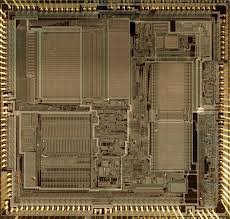
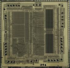
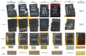
 Break Chip PIC16F716 Heximal
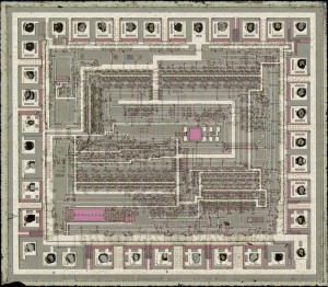
Break Chip PIC16F716 and extract Heximal out from MCU PIC16F716 flash memory, the security fuse bit of Microcontroller PIC16F716 can be removed or disable for the original MCU PIC16F716
Break Chip PIC16F716 and extract Heximal out from MCU PIC16F716 flash memory, the security fuse bit of Microcontroller PIC16F716 can be removed or disable for the original MCU PIC16F716;
Microcontroller Core Features:
· High-performance RISC CPU
· Only 35 single-word instructions to learn
– All single-cycle instructions except for
program branches which are two-cycle
· Operating speed: DC – 20 MHz clock input
DC – 200 ns instruction cycle
· Interrupt capability (up to 7 internal/external interrupt sources)
· 8-level deep hardware stack
· Direct, Indirect and Relative Addressing modes
Special Microcontroller Features:
· Power-on Reset (POR)
· Power-up Timer (PWRT) and
Oscillator Start-up Timer (OST)
· Watchdog Timer (WDT) with its own on-chip RC
oscillator for reliable operation
· Dual level Brown-out Reset circuitry
– 2.5 VBOR (Typical)
– 4.0 VBOR (Typical)
· Programmable code protection
· Power-Saving Sleep mode
· Selectable oscillator options
· Fully static design
· In-Circuit Serial Programming (ICSP™)
CMOS Technology:
· Wide operating voltage range:
– Industrial: 2.0V to 5.5V
– Extended: 3.0V to 5.5V
· High Sink/Source Current 25/25 mA
· Wide temperature range:
– Industrial: -40°C to 85°C
– Extended: -40°C to 125°C
Low-Power Features:
· Standby Current:
– 100 nA @ 2.0V, typical
· Operating Current:
– 14 ìA @ 32 kHz, 2.0V, typical
– 120 ìA @ 1 MHz, 2.0V, typical
– 1 ìA @ 2.0V, typical
· Timer1 Oscillator Current:
– 3.0 ìA @ 32 kHz, 2.0V, typical
Peripheral Features:
· Timer0: 8-bit timer/counter with 8-bit prescaler can be incremented during Sleep via external crystal/clock
· Timer2: 8-bit timer/counter with 8-bit period register, prescaler and postscaler
· Enhanced Capture, Compare, PWM module:
– Capture is 16-bit, max. resolution is 12.5 ns
– Compare is 16-bit, max. resolution is 200 ns
– PWM maximum resolution is 10-bit
– Enhanced PWM:
– Single, Half-Bridge and Full-Bridge modes
– Digitally programmable dead-band delay
– Auto-shutdown/restart
· 8-bit multi-channel Analog-to-Digital Converter
· 13 I/O pins with individual direction control
· Programmable weak pull-ups on PORTB
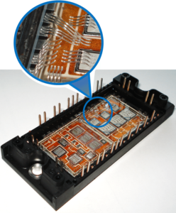
Break Microcontroller MC68376BACAB25 Program
We can Break Microcontroller MC68376BACAB25 Program, please view below Microcontroller MC68376BACAB25 features for your reference:
The MC68336 and the MC68376 are highly-integrated 32-bit microcontrollers, combining high-performance data manipulation capabilities with powerful peripheral subsystems.
MC68300 microcontrollers are built up from standard modules that interface through a common intermodule bus (IMB). Standardization facilitates rapid development of devices tailored for specific applications when Break Microcontroller.
The MC68336 incorporates a 32-bit CPU (CPU32), a system integration module (SIM), a time processor unit (TPU), a configurable timer module (CTM4), a queued serial module (QSM), a 10-bit queued analog-to-digital converter module (QADC), a 3.5-Kbyte TPU emulation RAM module (TPURAM), and a 4-Kbyte standby RAM module (SRAM) if Break Microcontroller.
The MC68376 includes all of the aforementioned modules, plus a CAN 2.0B protocol controller module (TouCAN™) and an 8-Kbyte masked ROM (MRM).
The MC68336/376 can either synthesize the system clock signal from a fast reference or use an external clock input directly after Break Microcontroller. Operation with a 4.194 MHz reference frequency is standard. The maximum system clock speed is 20.97 MHz. System hardware and software allow changes in clock rate during operation. Because MCU operation is fully static, register and memory contents are not affected by clock rate changes before Break Microcontroller.
High-density complementary metal-oxide semiconductor (HCMOS) architecture makes the basic power consumption of the MCU low. Power consumption can be minimized by stopping the system clock. The CPU32 instruction set includes a low-power stop (LPSTOP) instruction that efficiently implements this capability after Break Microcontroller.
Documentation for the Modular Microcontroller Family follows the modular construction of the devices in the product line. Each microcontroller has a comprehensive user’s manual that provides sufficient information for normal operation of the device before Break Microcontroller.
The user’s manual is supplemented by module reference manuals that provide detailed information about module operation and applications. Refer to Motorola publication Advanced Microcontroller Unit (AMCU) Literature (BR1116/D) for a complete listing of documentation when Break IC.
Break MCU MC68HC11F1CFN3 Heximal
Break MCU MC68HC11F1CFN3 tamper resistance system and read heximal file out from Microcontroller MC68HC11F1, status of Microprocessor will be reset from locked to unlocked one
Break MCU MC68HC11F1CFN3 tamper resistance system and read heximal file out from Microcontroller MC68HC11F1, status of Microprocessor will be reset from locked to unlocked one;
Features
· MC68HC11 CPU
· Power Saving STOP and WAIT Modes
· 4 Kbytes of On-Chip ROM
· 192 Bytes of On-Chip RAM (All Saved During Standby)
· 16-Bit Timer System
— 3 Input Capture (IC) Channels
— 4 Output Compare (OC) Channels
— One IC or OC Channel (Software Selectable)
· 8-Bit Pulse Accumulator
· Real-Time Interrupt Circuit
· Computer Operating Properly (COP) Watchdog System
· Synchronous Serial Peripheral Interface (SPI)
· Asynchronous Nonreturn to Zero (NRZ) Serial Communications Interface (SCI)
· 26 Input/Output (I/O) Pins
— 16 Bidirectional I/O Pins
— 3 Input Only Pins
— 3 Output Only Pins (One Output Only Pin in the 40-Pin Package)
· Available in a 44-Pin Plastic Leaded Chip Carrier (PLCC) and 40-Pin Dual In-Line Package (DIP) 2.1 VDD, VSS, and EVSS
Power is supplied to the MCU through VDD and VSS. VSS is the power supply, and VSS is ground. EVSS, available on the 44-pin PLCC, is an additional ground pin that must be grounded with VSS. The MCU operates from a single 5-volt (nominal) power supply. Very fast signal transitions occur on the MCU pins. The short rise and fall times place high, short duration current demands on the power supply. To prevent noise problems, provide good power supply bypassing at the MCU. Also, use bypass capacitors that have good high-frequency characteristics and situate them as close to the MCU as possible. Bypass requirements vary, depending on how heavily the MCU pins are loaded.
2.2 Reset (RESET)
An active low bidirectional control signal, RESET, acts as an input to initialize the MCU to a known startup state. It also acts as an open-drain output to indicate that an internal failure has been detected in either the clock monitor or COP watchdog circuit. The CPU distinguishes between internal and external reset conditions by sensing whether the reset pin rises to a logic one in less than two E-clock cycles after a reset has occurred. It is not advisable to connect an external resistor-capacitor (RC) power-up delay circuit to the reset pin of M68HC11 devices because the circuit charge time 2.3 Crystal Driver and External Clock Input (XTAL, EXTAL)
These two pins provide the interface for either a crystal or a CMOS compatible clock to control the internal clock generator circuitry. The frequency applied to these pins is four times higher than the desired E-clock rate.
The XTAL pin is normally left unterminated when an external CMOS compatible clock input is connected to the EXTAL pin. However, a 10 kΩ to 100 kΩ load resistor connected from XTAL to ground can be used to reduce RFI noise emission. The XTAL output is normally intended to drive only a crystal. The XTAL output can be buffered with a high impedance buffer, or it can be used to drive the EXTAL input of another M68HC11.
Break IC LPC2132FBD64 Firmware
Break IC LPC2132FBD64 program memory and readout firmware from Microcontroller
Break IC LPC2132FBD64 program memory and readout firmware from Microcontroller LPC2132FBD64, focus ion beam technique will be applied to reset the status of MCU LPC2132FBD64 from locked to unlocked one;
The LPC2132 microcontrollers are based on a 32/16 bit ARM7TDMI-S CPU with real-time emulation and embedded trace support, that combines the microcontroller with 32 kB, 64 kB, 128 kB, 256 kB and 512 kB of embedded high speed Flash memory.
A 128-bit wide memory interface and a unique accelerator architecture enable 32-bit code execution at maximum clock rate. For critical code size applications, the alternative 16-bit Thumb mode reduces code by more than 30 % with minimal performance penalty after Copying IC PIC16F84A binary.
Due to their tiny size and low power consumption, these microcontrollers are ideal for applications where miniaturization is a key requirement, such as access control and point-of-sale. With a wide range of serial communications interfaces and on-chip SRAM options of 8/16/32 kB, they are very well suited for communication gateways and protocol converters, soft modems, voice recognition and low end imaging, providing both large buffer size and high processing power. Various 32-bit timers, single or dual 10-bit 8 channel ADC(s), 10-bit DAC, PWM channels and 47 GPIO lines with up to nine edge or level sensitive external interrupt pins make these microcontrollers particularly suitable for industrial control and medical systems after attacking C8051F530 firmware.
16/32-bit ARM7TDMI-S microcontroller in a tiny LQFP64 package.
8/16/32 kB of on-chip static RAM and 32/64/128/256/512 kB of on-chip Flash program memory. 128 bit wide interface/accelerator enables high speed 60 MHz operation. In-System/In-Application Programming (ISP/IAP) via on-chip boot-loader software.
Single Flash sector or full chip erase in 400 ms and programming of 256 bytes in 1 ms. EmbeddedICE RT and Embedded Trace interfaces offer real-time debugging with the on-chip RealMonitor software and high speed tracing of instruction execution.
One (LPC2132) or two (LPC2134/36/38) 8 channel 10-bit A/D converters provides a total of up to 16 analog inputs, with conversion times as low as 2.44 µs per channel. Single 10-bit D/A converter provides variable analog output (LPC2132). Two 32-bit timers/external event counters (with four capture and four compare channels each), PWM unit (six outputs) and watchdog after attack microcontroller PIC16C63A heximal.
Low power Real-time clock with independent power and dedicated 32 kHz clock input.
Multiple serial interfaces including two UARTs (16C550), two Fast I2C-bus (400 kbit/s),
SPI and SSP with buffering and variable data length capabilities.
Vectored interrupt controller with configurable priorities and vector addresses.
Up to 47 5 V tolerant general purpose I/O pins in tiny LQFP64 package.
Up to nine edge or level sensitive external interrupt pins available.
60 MHz maximum CPU clock available from programmable on-chip PLL with settling time of 100 µs.
On-chip integrated oscillator operates with external crystal in range of 1 MHz to
30 MHz and with external oscillator up to 50 MHz.
Power saving modes include Idle and Power-down
Individual enable/disable of peripheral functions as well as peripheral clock scaling down for additional power optimization.
Processor wake-up from Power-down mode via external interrupt or BOD.
Single power supply chip with POR and BOD circuits:
CPU operating voltage range of 3.0 V to 3.6 V (3.3 V ± 10 %) with 5 V tolerant I/O pads.
Recover Chip MC68HC11A0FN3 Binary
Recover Chip MC68HC11A0FN3 Binary from Microcontroller MC68HC11A0FN3 program memory, unlock microprocessor MC68HC11A0FN3 security fuse bit and extract heximal out from memory
Recover Chip MC68HC11A0FN3 Binary from Microcontroller MC68HC11A0FN3 program memory, unlock microprocessor MC68HC11A0FN3 security fuse bit and extract heximal out from memory;
· Power Saving STOP and WAIT Modes
· 4 Kbytes of On-Chip ROM
· 192 Bytes of On-Chip RAM (All Saved During Standby)
· 16-Bit Timer System
— 3 Input Capture (IC) Channels
— 4 Output Compare (OC) Channels
— One IC or OC Channel (Software Selectable)
· 8-Bit Pulse Accumulator
· Real-Time Interrupt Circuit
· Computer Operating Properly (COP) Watchdog System
· Synchronous Serial Peripheral Interface (SPI)
· Asynchronous Nonreturn to Zero (NRZ) Serial Communications Interface (SCI)
· 26 Input/Output (I/O) Pins
— 16 Bidirectional I/O Pins
— 3 Input Only Pins
— 3 Output Only Pins (One Output Only Pin in the 40-Pin Package)
· Available in a 44-Pin Plastic Leaded Chip Carrier (PLCC) and 40-Pin Dual In-Line Package (DIP)
2.1 VDD, VSS, and EVSS
Power is supplied to the MCU through VDD and VSS. VSS is the power supply, and VSS is ground. EVSS, available on the 44-pin PLCC, is an additional ground pin that must be grounded with VSS. The MCU operates from a single 5-volt (nominal) power supply before MCU PIC32MX440F512H binary copying. Very fast signal transitions occur on the MCU pins.
The short rise and fall times place high, short duration current demands on the power supply. To prevent noise problems, provide good power supply bypassing at the MCU. Also, use bypass capacitors that have good high-frequency characteristics and situate them as close to the MCU as possible. Bypass requirements vary, depending on how heavily the MCU pins are loaded.
2.2 Reset (RESET)
An active low bidirectional control signal, RESET, acts as an input to initialize the MCU to a known startup state. It also acts as an open-drain output to indicate that an internal failure has been detected in either the clock monitor or COP watchdog circuit. The CPU distinguishes between internal and external reset conditions by sensing whether the reset pin rises to a logic one in less than two E-clock cycles after a reset has occurred. It is not advisable to connect an external resistor-capacitor (RC) power-up delay circuit to the reset pin of M68HC11 devices because the circuit charge time.
2.3 Crystal Driver and External Clock Input (XTAL, EXTAL)
These two pins provide the interface for either a crystal or a CMOS compatible clock to control the internal clock generator circuitry. The frequency applied to these pins is four times higher than the desired E-clock rate after Recover MCU PIC16F913 bin.
The XTAL pin is normally left unterminated when an external CMOS compatible clock input is connected to the EXTAL pin. However, a 10 kΩ to 100 kΩ load resistor connected from XTAL to ground can be used to reduce RFI noise emission. The XTAL output is normally intended to drive only a crystal. The XTAL output can be buffered with a high impedance buffer, or it can be used to drive the EXTAL input of another M68HC11.
Recover Microcontroller 430G2452 Heximal
Recover Microcontroller 430G2452 Heximal out from MCU MSP430G2452 is a process start from Crack MCU MSP430G2452 protective system and disable its security fuse bit by focus ion beam, then copy the code fro new microcontroller
Recover Microcontroller 430G2452 Heximal out from MCU MSP430G2452 is a process start from Crack MCU MSP430G2452 protective system and disable its security fuse bit by focus ion beam, then copy the code fro new microcontroller;
FEATURES
Low Supply Voltage Range: 1.8 V to 3.6 V Ultra-Low Power Consumption
– Active Mode: 220 µA at 1 MHz, 2.2 V
– Standby Mode: 0.5 µA
– Off Mode (RAM Retention): 0.1 µA
Five Power-Saving Modes Ultra-Fast Wake-Up From Standby Mode in Less Than 1 µs 16-Bit RISC Architecture, 62.5-ns Instruction Cycle Time.
Basic Clock Module Configurations
– Internal Frequencies up to 16 MHz With
Four Calibrated Frequencies
– Internal Very-Low-Power Low-Frequency (LF) Oscillator
– 32-kHz Crystal
– External Digital Clock Source
One 16-Bit Timer_A With Three Capture/Compare Registers Up to 16 Touch-Sense Enabled I/O Pins
Universal Serial Interface (USI) Supporting SPI and I2C 10-Bit 200-ksps Analog-to-Digital (A/D)
Converter With Internal Reference, Sample-and-Hold, and Autoscan (MSP430G2x52 Only) On-Chip Comparator for Analog Brownout Detector Serial Onboard Programming, No External Programming Voltage Needed, Programmable Code Protection by Security Fuse On-Chip Emulation Logic With Spy-Bi-Wire Interface Family Members are Summarized:
Package Options
– TSSOP: 14 Pin, 20 Pin
– PDIP: 20 Pin
– QFN: 16 Pin
For Complete Module Descriptions, See the MSP430x2xx Family User’s Guide (SLAU144)
DESCRIPTION
The Texas Instruments MSP430™ family of ultra-low-power microcontrollers consist of several devices featuring different sets of peripherals targeted for various applications. The architecture, combined with five low-power modes, is optimized to achieve extended battery life in portable measurement applications.
The device features a powerful 16-bit RISC CPU, 16-bit registers, and constant generators that contribute to maximum code efficiency. The digitally controlled oscillator (DCO) allows wake-up from low-power modes to active mode in less than 1 µs.
The MSP430G2x52 and MSP430G2x12 series of microcontrollers are ultra-low-power mixed signal microcontrollers with built-in 16-bit timers, and up to 16 I/O touch sense enabled pins and built-in communication capability using the universal serial communication interface and have a versatile analog comparator.
The MSP430G2x52 series have a 10-bit A/D converter. For configuration details see Table 1. Typical applications include low-cost sensor systems that capture analog signals, convert them to digital values, and then process the data for display or for transmission to a host system when attacking Microcontrolle ST62T15C6 firmware memory.
Recover MCU PIC18F2520 Binary
Recover MCU PIC18F2520 Binary from Microcontroller PIC18F2520 program memory, reset the security fuse bit inside the protective system from locked to unlocked one by Crack MCU PIC18F2520
Recover MCU PIC18F2520 Binary from Microcontroller PIC18F2520 program memory, reset the security fuse bit inside the protective system from locked to unlocked one by Crack MCU PIC18F2520;
Power Management Features:
Peripheral Highlights (Continued):
Run: CPU on, Peripherals on
Idle: CPU off, Peripherals on
Sleep: CPU off, Peripherals off
Ultra Low 50nA Input Leakage
Run mode Currents Down to 11 ìA Typical
Idle mode Currents Down to 2.5 ìA Typical
Sleep mode Current Down to 100 nA Typical
Timer1 Oscillator: 900 nA, 32 kHz, 2V
Watchdog Timer: 1.4 ìA, 2V Typical
Two-Speed Oscillator Start-up
· Master Synchronous Serial Port (MSSP) module
Supporting 3-Wire SPI (all 4 modes) and I2C™
Master and Slave modes
· Enhanced Addressable USART module:
– Supports RS-485, RS-232 and LIN/J2602
– RS-232 operation using internal oscillator block (no external crystal required)
– Auto-wake-up on Start bit
– Auto-Baud Detect
· 10-Bit, up to 13-Channel Analog-to-Digital (A/D)
Flexible Oscillator Structure:
· Four Crystal modes, up to 40 MHz
· 4x Phase Lock Loop (PLL) – Available for Crystal and Internal Oscillators
· Two External RC modes, up to 4 MHz
· Two External Clock modes, up to 40 MHz
· Internal Oscillator Block:
– Fast wake from Sleep and Idle, 1 ìs typical
– 8 use-selectable frequencies, from 31 kHz to 8 MHz
– Provides a complete range of clock speeds from 31 kHz to 32 MHz when used with PLL
– User-tunable to compensate for frequency drift
· Secondary Oscillator using Timer1 @ 32 kHz
· Fail-Safe Clock Monitor:
– Allows for safe shutdown if peripheral clock stops
Peripheral Highlights:
Converter module:
– Auto-acquisition capability
– Conversion available during Sleep
· Dual Analog Comparators with Input Multiplexing
· Programmable 16-Level High/Low-Voltage
Detection (HLVD) module:
– Supports interrupt on High/Low-Voltage Detection
Special Microcontroller Features:
· C Compiler Optimized Architecture:
– Optional extended instruction set designed to
optimize re-entrant code
· 100,000 Erase/Write Cycle Enhanced Flash
Program Memory Typical
· 1,000,000 Erase/Write Cycle Data EEPROM
Memory Typical
· Flash/Data EEPROM Retention: 100 Years Typical
· Self-Programmable under Software Control
High-Current Sink/Source 25 mA/25 mA
Three Programmable External Interrupts
Four Input Change Interrupts
Up to 2 Capture/Compare/PWM (CCP) modules,
· Priority Levels for Interrupts
· 8 x 8 Single-Cycle Hardware Multiplier
· Extended Watchdog Timer (WDT):
– Programmable period from 4 ms to 131s one with Auto-Shutdown (28-pin devices)
· Enhanced Capture/Compare/PWM (ECCP) module (40/44-pin devices only):
– One, two or four PWM outputs
– Selectable polarity
– Programmable dead time
– Auto-shutdown and auto-restart
· Single-Supply 5V In-Circuit Serial
Programming™ (ICSP™) via Two Pins
· In-Circuit Debug (ICD) via Two Pins
· Wide Operating Voltage Range: 2.0V to 5.5V
· Programmable Brown-out Reset (BOR) with
Software Enable Option
Recover IC AT89C4051 Heximal
Recover IC AT89C4051 Heximal from flash memory and eeprom memory, decapsulate MCU AT89C4051 silicon package by MCU cracking, so the microprobe will be able to get access to the databus of Microcontroller AT89C4051
Recover IC AT89C4051 Heximal from flash memory and eeprom memory, decapsulate MCU AT89C4051 silicon package by MCU cracking, so the microprobe will be able to get access to the databus of Microcontroller AT89C4051;
Features
· Compatible with MCS®51 Products
· 4K Bytes of Reprogrammable Flash Memory
– Endurance: 1,000 Write/Erase Cycles
2.7V to 6V Operating Range
Fully Static Operation: 0 Hz to 24 MHz
Two-level Program Memory Lock
128 x 8-bit Internal RAM
15 Programmable I/O Lines
Two 16-bit Timer/Counters
Six Interrupt Sources
Programmable Serial UART Channel
Direct LED Drive Outputs
On-chip Analog Comparator
Low-power Idle and Power-down Modes
Brown-out Detection
Power-On Reset (POR)
Green (Pb/Halide-free/RoHS Compliant) Packaging
The AT89C4051 is a low-voltage, high-performance CMOS 8-bit microcontroller with
4K bytes of Flash programmable and erasable read-only memory. The device is manufactured using Atmel’s high-density nonvolatile memory technology and is compatible with the industry-standard MCS-51 instruction set. By combining a versatile 8-bit CPU with Flash on a monolithic chip, the Atmel AT89C4051 is a powerful microcontroller which provides a highly-flexible and cost-effective solution to many embedded control applications.
The AT89C4051 provides the following standard features: 4K bytes of Flash, 128 bytes of RAM, 15 I/O lines, two 16-bit timer/counters, a five-vector, two-level interrupt architecture, a full duplex serial port, a precision analog comparator, on-chip oscillator and clock circuitry. In addition, the AT89C4051 is designed with static logic for operation down to zero frequency and supports two software-selectable power saving modes. The Idle Mode stops the CPU while allowing the RAM, timer/counters, serial port and interrupt system to continue functioning. The power-down mode saves the RAM contents but freezes the oscillator disabling all other chip functions until the next hardware reset for MCU Attacking.
Circuit Engineering Company Limited continues to be recognized as the Southern China Leader in Services for IC Break, MCU attack, Chip Recover, Microcontroller Copy service. With the advancement of today’s modern circuit board technology, it is more important than ever to have specialists available to help you at a moment’s notice. Our engineering and commercial teams collectively have a vast amount of electronic experience covering field include Consumer Electronics, Industrial Automation Electronics, Wireless Communication Electronics., etc. For more information please contact us through email.
Copy Microcontroller P87C51X2BBD Binary
Copy Microcontroller P87C51X2BBD Binary from locked memory include flash and eeprom, remove the security fuse bit of MCU P87C51X2 by MCU Cracking technology and readout firmware from opened Microprocessor
Copy Microcontroller P87C51X2BBD Binary from locked memory include flash and eeprom, remove the security fuse bit of MCU P87C51X2 by MCU Cracking technology and readout firmware from opened Microprocessor;
FEATURES
· 80C51 Central Processing Unit
– 4 kbytes ROM/EPROM (P80/P87C51X2)
– 8 kbytes ROM/EPROM (P80/P87C52X2)
– 16 kbytes ROM/EPROM (P80/P87C54X2)
– 32 kbytes ROM/EPROM (P80/P87C58X2)
– 128 byte RAM (P80/P87C51X2 and P80C31X2)
– 256 byte RAM (P80/P87C52/54X2/58X2 and P80C32X2)
– Boolean processor
– Fully static operation
– Low voltage (2.7 V to 5.5 V at 16 MHz) operation
· 12-clock operation with selectable 6-clock operation (via software or via parallel programmer)
· Memory addressing capability
– Up to 64 kbytes ROM and 64 kbytes RAM
· Power control modes:
– Clock can be stopped and resumed
– Idle mode
– Power-down mode
· CMOS and TTL compatible
· Two speed ranges at VCC = 5 V
– 0 to 30 MHz with 6-clock operation
– 0 to 33 MHz with 12-clock operation
· PLCC, DIP, TSSOP or LQFP packages
· Extended temperature ranges
· Dual Data Pointers
· Security bits:
– ROM (2 bits)
– OTP (3 bits)
· Encryption array – 64 bytes
· Four interrupt priority levels
· Six interrupt sources
· Four 8-bit I/O ports
· Full-duplex enhanced UART
– Framing error detection
– Automatic address recognition
· Three 16-bit timers/counters T0, T1 (standard 80C51) and additional T2 (capture and compare)
· Programmable clock-out pin
· Asynchronous port reset
· Low EMI (inhibit ALE, slew rate controlled outputs, and 6-clock mode)
· Wake-up from Power Down by an external interrupt.
Circuit Engineering Company Limited continues to be recognized as the Southern China Leader in Services for IC Break, MCU recover, Chip Recover, Microcontroller Copy service. With the advancement of today’s modern circuit board technology, it is more important than ever to have specialists available to help you at a moment’s notice. Our engineering and commercial teams collectively have a vast amount of electronic experience covering field include Consumer Electronics, Industrial Automation Electronics, Wireless Communication Electronics., etc. For more information please contact us through email.
Copy MCU ATmega32A Software
Copy MCU ATmega32A Software from master microcontroller ATmega32A program memory, and reprogramme the firmware into blank new Microprocessor ATmega32A for MCU cloning;
Copy MCU ATmega32A Software from master microcontroller ATmega32A program memory, and reprogramme the firmware into blank new Microprocessor ATmega32A for MCU cloning
Features
· High-performance, Low-power AVR® 8-bit Microcontroller
· Advanced RISC Architecture
– 131 Powerful Instructions – Most Single-clock Cycle Execution
– 32 x 8 General Purpose Working Registers
– Fully Static Operation
– Up to 16 MIPS Throughput at 16 MHz
– On-chip 2-cycle Multiplier
High Endurance Non-volatile Memory segments
– 32K Bytes of In-System Self-programmable Flash program memory after firmware MCU PIC16F84 extraction
– 1024 Bytes EEPROM
– 2K Byte Internal SRAM
– Write/Erase Cycles: 10,000 Flash/100,000 EEPROM
– Data retention: 20 years at 85°C/100 years at 25°C(1)
– Optional Boot Code Section with Independent Lock Bits
· In-System Programming by On-chip Boot Program
· True Read-While-Write Operation
– Programming Lock for Software Security
JTAG (IEEE std. 1149.1 Compliant) Interface
– Boundary-scan Capabilities According to the JTAG Standard
– Extensive On-chip Debug Support
– Programming of Flash, EEPROM, Fuses, and Lock Bits through the JTAG Interface
Peripheral Features
– Two 8-bit Timer/Counters with Separate Prescalers and Compare Modes
– One 16-bit Timer/Counter with Separate Prescaler, Compare Mode, and Capture Mode
– Real Time Counter with Separate Oscillator
– Four PWM Channels
– 8-channel, 10-bit ADC
· 8 Single-ended Channels
· 7 Differential Channels in TQFP Package Only
· 2 Differential Channels with Programmable Gain at 1x, 10x, or 200x
– Byte-oriented Two-wire Serial Interface
– Programmable Serial USART
– Master/Slave SPI Serial Interface
– Programmable Watchdog Timer with Separate On-chip Oscillator
– On-chip Analog Comparator
Special Microcontroller Features
– Power-on Reset and Programmable Brown-out Detection
– Internal Calibrated RC Oscillator
– External and Internal Interrupt Sources
– Six Sleep Modes: Idle, ADC Noise Reduction, Power-save, Power-down, Standby and Extended Standby
I/O and Packages
– 32 Programmable I/O Lines
– 40-pin PDIP, 44-lead TQFP, and 44-pad QFN/MLF
Operating Voltages
– 2.7 – 5.5V for ATmega32A
Speed Grades
– 0 – 16 MHz for ATmega32A
Power Consumption at 1 MHz, 3V, 25°C for ATmega32A
Summary
– Active: 0.6 mA
– Idle Mode: 0.2 mA
– Power-down Mode: < 1 µA