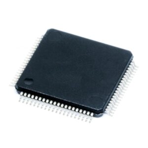
 Reverse Engineer DSP TMS320F28030PAG Microcontroller Flash Memory
Reverse Engineer DSP TMS320F28030PAG Microcontroller Flash Memory and restore dsp cpu tms320f28030pagt source code, copy flash program to new tms320f28030pag texas instrument dsp mcu;
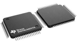
Reverse Engineer DSP TMS320F28030PAG Microcontroller Flash Memory and restore dsp cpu tms320f28030pagt source code, copy flash program to new tms320f28030pag texas instrument dsp mcu
Section 6.2.1 describes the signals. With the exception of the JTAG pins, the GPIO function is the default at reset, unless otherwise mentioned. The peripheral signals that are listed under them are alternate functions. Some peripheral functions may not be available in all devices. See Table 5-1 for details. Inputs are not 5-V tolerant. All GPIO pins are I/O/Z and have an internal pullup, which can be selectively enabled/disabled on a per-pin basis. This feature only applies to the GPIO pins. The pullups on the PWM pins are not enabled at reset. The pullups on other GPIO pins are enabled upon reset. The AIO pins do not have an internal pullup.

memoria flash del microcontrolador DSP TMS320F28030PAG de ingeniería inversa y restauración del código fuente dsp cpu tms320f28030pagt, copia del programa flash al nuevo instrumento tms320f28030pag texas dsp mcu;
When the on-chip VREG is used, the GPIO19, GPIO34, GPIO35, GPIO36, GPIO37, and GPIO38 pins could glitch during power up. This potential glitch will finish before the boot mode pins are read and will not affect boot behavior. If glitching is unacceptable in an application, 1.8 V could be supplied externally.
Alternatively, adding a current-limiting resistor (for example, 470 Ω) in series with these pins and any external driver could be considered to limit the potential for degradation to the pin and/or external circuitry. There is no power-sequencing requirement when using an external 1.8-V supply. However, if the 3.3-V transistors in the level-shifting output buffers of the I/O pins are powered before the 1.8-V transistors, it is possible for the output buffers to turn on, causing a glitch to occur on the pin during power up. To avoid this behavior, power the VDD pins before or with the VDDIO pins, ensuring that the VDD pins have reached 0.7 V before the VDDIO pins reach 0.7 V.
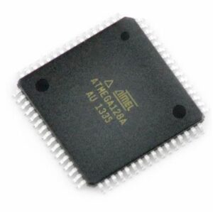
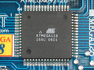
 Encrypted ATMEL ATMEGA128A MCU Flash Decoding
Encrypted ATMEL ATMEGA128A MCU Flash Decoding will help engineer to copy atmega128a microcontroller flash heximal file out after readout atmega128a microprocessor’s content software from its flash and eeprom memory;
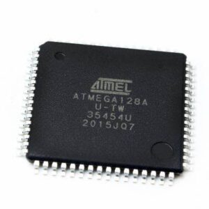
Encrypted ATMEL ATMEGA128A MCU Flash Decoding will help engineer to copy atmega128a microcontroller flash heximal file out after readout atmega128a microprocessor’s content software from its flash and eeprom memory
In this mode, the Watchdog Timer is always enabled, and the WDE bit will always read as one. A timed sequence is needed when changing the Watchdog Time-out period. To change the Watchdog Time-out, the following procedure must be followed:
- In the same operation, write a logical one to WDCE and WDE. Even though the WDE always is set, the WDE must be written to one to start the timed sequence
Within the next four clock cycles, in the same operation, write the WDP bits as desired, but with the WDCE bit cleared. The value written to the WDE bit is irrelevant to break atmega128a mcu fuse bit inside the flash memory.
La decodificación flash MCU ATMEL ATMEGA128A cifrada ayudará al ingeniero a copiar el archivo heximal flash del microcontrolador atmega128a después de leer el software de contenido del microprocesador atmega128a de su memoria flash y eeprom
This section describes the specifics of the interrupt handling performed by the ATmega8. For a general explanation of the AVR interrupt handling, refer to “Reset and Interrupt Handling” on page 14.
Table 19 on page 47 shows reset and Interrupt Vectors placement for the various combinations of BOOTRST and IVSEL settings. If the program never enables an interrupt source, the Interrupt Vectors are not used, and regular program code can be placed at these locations. This is also the case if the Reset Vector is in the Application section while the Interrupt Vectors are in the boot section or vice versa to break atmega128a ic chip flash memory.
- When the BOOTRST Fuse is programmed, the device will jump to the Boot Loader address at reset, see “Boot Loader Support – Read-While-Write Self-Programming” on page 202
- When the IVSEL bit in GICR is set, Interrupt Vectors will be moved to the start of the boot Flash The address of each Interrupt Vector will then be the address in this table added to the start address of the boot Flash section;
- The Boot Reset Address is shown in Table 82 on page 213. For the BOOTRST Fuse “1” means unprogrammed while “0” means programmed
The most typical and general program setup for the Reset and Interrupt Vector Addresses in ATmega128A is:
| addressLabels | Code | Comments | ||
| $000 | rjmp | RESET | ; Reset Handler | |
| $001 | rjmp | EXT_INT0 | ; IRQ0 Handler | |
| $002 | rjmp | EXT_INT1 | ; IRQ1 Handler | |
| $003 | rjmp | TIM2_COMP | ; Timer2 Compare Handler | |
| $004 | rjmp | TIM2_OVF | ; Timer2 Overflow Handler | |
| $005 | rjmp | TIM1_CAPT | ; Timer1 Capture Handler | |
| $006 | rjmp | TIM1_COMPA | ; Timer1 CompareA Handler | |
| $007 | rjmp | TIM1_COMPB | ; Timer1 CompareB Handler | |
| $008 | rjmp | TIM1_OVF | ; Timer1 Overflow Handler | |
| $009 | rjmp | TIM0_OVF | ; Timer0 Overflow Handler | |
| $00a | rjmp | SPI_STC | ; SPI Transfer Complete Handler | |
| $00b | rjmp | USART_RXC | ; USART RX Complete Handler | |
| $00c | rjmp | USART_UDRE | ; UDR Empty Handler | |
| $00d | rjmp | USART_TXC | ; USART TX Complete Handler | |
| $00e | rjmp | ADC | ; ADC Conversion Complete Handler | |
| $00f | rjmp | EE_RDY | ; EEPROM Ready Handler | |
| $010 | rjmp | ANA_COMP | ; Analog Comparator Handler | |
| $011 | rjmp | TWSI | ; Two-wire Serial Interface Handler | |
| $012 | rjmp | SPM_RDY | ; Store Program Memory Ready Handler | |
| ; | ||||
| $013 | RESET: ldi | r16,high(RAMEND); Main program start | ||
| $014 | out | SPH,r16 ; Set Stack Pointer to top of RAM | ||
| $015 | ldi | r16,low(RAMEND) | ||
| $016 | out | SPL,r16 | ||
| $017 | sei | ; Enable interrupts | ||
| $018 | <instr> xxx | |||
| … | … | … | ||
 Crack Locked ATMEGA128L AVR Chip
Crack Locked ATMEGA128L AVR Chip and readout atmega128l microcontroller flash memory firmware, the secured heximal file of atmega128l mcu can be deciphered from its flash memory;
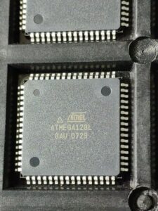
Crack Locked ATMEGA128L AVR Chip and readout atmega128l microcontroller flash memory firmware, the secured heximal file of atmega128l mcu can be deciphered from its flash memory;
When the WDE is written to logic one, the Watchdog Timer is enabled, and if the WDE is written to logic zero, the Watchdog Timer function is disabled to break off atmega128l chipset fuse bit. WDE can only be cleared if the WDCE bit has logic level one. To disable an enabled Watchdog Timer, the following procedure must be followed:
- In the same operation, write a logic one to WDCE and WDE. A logic one must be written to WDE even though it is set to one before the disable operation starts
- Within the next four clock cycles, write a logic 0 to This disables the Watchdog
- Bits .0 – WDP2, WDP1, WDP0: Watchdog Timer Prescaler 2, 1, and 0
The WDP2, WDP1, and WDP0 bits determine the Watchdog Timer prescaling when the Watch- dog Timer is enabled. The different prescaling values and their corresponding Timeout Periods are shown in Table 17.
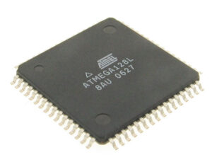
rompa el chip ATMEGA128L avr bloqueado y lea el firmware de la memoria flash del microcontrolador atmega128l, el archivo heximal seguro de atmega128l mcu se puede descifrar desde su memoria flash
The following code example shows one assembly and one C function for turning off the WDT. The example assumes that interrupts are controlled (for example, by disabling interrupts glob- ally) so that no interrupts will occur during execution of these functions.
In this mode, the Watchdog Timer is initially disabled, but can be enabled by writing the WDE bit to 1 without any restriction. A timed sequence is needed when changing the Watchdog Time-out period or disabling an enabled Watchdog Timer by breaking atmega128l microcontroller flash memory. To disable an enabled Watchdog Timer and/or changing the Watchdog Time-out, the following procedure must be followed:
- In the same operation, write a logic one to WDCE and WDE. A logic one must be written to WDE regardless of the previous value of the WDE bit
- Within the next four clock cycles, in the same operation, write the WDE and WDP bits as desired, but with the WDCE bit cleared
 Copy AVR Microcontroller ATMEGA128 Flash Heximal
Copy AVR Microcontroller ATMEGA128 Flash Heximal needs to unlock avr secured mcu atmega128 protection, the un-encrypted avr microprocessor atmega128 flash memory binary will be extracted;
Copy AVR Microcontroller ATMEGA128 Flash Heximal needs to unlock avr secured mcu atmega128 protection, the un-encrypted avr microprocessor atmega128 flash memory binary will be extracted
The Power-on Reset will not work unless the supply voltage has been below VPOT (falling), VBOT may be below nominal minimum operating voltage for some devices. For devices where this is the case, the device is tested down to VCC = VBOT during the production test to break avr atmega128 mcu fuse bit and readout program. This guarantees that a Brown-out Reset will occur before VCC drops to a voltage where correct operation of the microcontroller is no longer guaranteed. The test is performed using BOD-LEVEL = 1 for ATmega8L and BODLEVEL = 0 for ATmega8. BODLEVEL = 1 is not applicable for ATmega128;
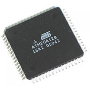
copia AVR microcontrolador ATMEGA128 flash heximal necesita para desbloquear avr asegurado mcu atmega128 protección, el no cifrado avr microprocesador atmega128 memoria flash binario será extraído;
A Power-on Reset (POR) pulse is generated by an On-chip detection circuit. The detection level is defined in Table 15 on page 38. The POR is activated whenever VCC is below the detection level. The POR circuit can be used to trigger the Start-up Reset, as well as to detect a failure in supply voltage.
A Power-on Reset (POR) circuit ensures that the device is reset from Power-on. Reaching the Power-on Reset threshold voltage invokes the delay counter when break atmega128 microcontroller firmware, which determines how long the device is kept in RESET after VCC rise. The RESET signal is activated again, without any delay, when VCC decreases below the detection level.
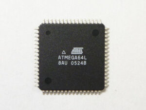
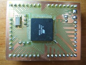
 Locked AVR Chip ATMEGA64A Heximal Duplication
Locked AVR Chip ATMEGA64A Heximal Duplication means original microcontroller atmega64a will be unlocked and embedded firmware of opened atmega64a microprocessor flash memory will be readout;
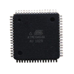
Locked AVR Chip ATMEGA64A Heximal Duplication means original microcontroller atmega64a will be unlocked and embedded firmware of opened atmega64a microprocessor flash memory will be readout
When the SM2..0 bits are written to 010, the SLEEP instruction makes the MCU enter Power- down mode. In this mode, the External Oscillator is stopped, while the external interrupts, the Two-wire Serial Interface address watch, and the Watchdog continue operating (if enabled).
Only an External Reset, a Watchdog Reset, a Brown-out Reset, a Two-wire Serial Interface address match interrupt, or an external level interrupt on INT0 or INT1, can wake up the MCU. This sleep mode basically halts all generated clocks, allowing operation of asynchronous mod- ules only.
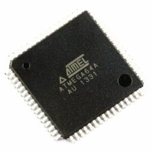
bloqueado chip AVR ATMEGA64A duplicación heximal significa microcontrolador original atmega64a será desbloqueado y el firmware incrustado de la memoria flash del microprocesador atmega64a abierto será readout;
Note that if a level triggered interrupt is used for wake-up from Power-down mode, the changed level must be held for some time to wake up the MCU. Refer to “External Interrupts” on page 66 for details of breaking off avr atmega64a flash memory binary program.
When waking up from Power-down mode, there is a delay from the wake-up condition occurs until the wake-up becomes effective. This allows the clock to restart and become stable after having been stopped. The wake-up period is defined by the same CKSEL Fuses that define the Reset Time-out period, as described in “Clock Sources” on page 26.
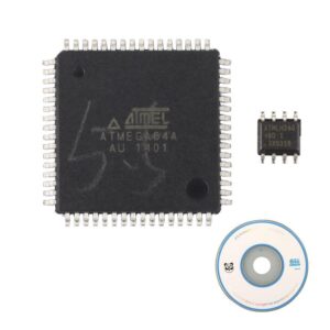
reverse atmega64a avr microcontroller protection and clone atmega64a avr mcu flash and eeprom memory data
When the SM2..0 bits are written to 011, the SLEEP instruction makes the MCU enter Power- save mode. This mode is identical to Power-down, with one exception:
If Timer/Counter2 is clocked asynchronously, that is, the AS2 bit in ASSR is set, Timer/Counter2 will run during sleep. The device can wake up from either Timer Overflow or Output Compare event from Timer/Counter2 if the corresponding Timer/Counter2 interrupt enable bits are set in TIMSK in the process of decrypting microcontroller atmega64a memory data, and the global interrupt enable bit in SREG is set.
 Secured AVR Microcontroller ATMEGA64L Binary Replication
Secured AVR Microcontroller ATMEGA64L Binary Replication will need to attack avr atmega64l encrypted mcu fuse bit then readout embedded firmware from atmega64l microprocessor flash memory;
Secured AVR Microcontroller ATMEGA64L Binary Replication will need to attack avr atmega64l encrypted mcu fuse bit then readout embedded firmware from atmega64l microprocessor flash memory
Idle mode enables the MCU to wake up from external triggered interrupts as well as internal ones like the Timer Overflow and USART Transmit Complete interrupts. If wake-up from the Analog Comparator interrupt is not required, the Analog Comparator can be powered down by setting the ACD bit in the Analog Comparator Control and Status Register – ACSR when break off secured microcontroller atmega64l flash memory. This will reduce power consumption in Idle mode. If the ADC is enabled, a conversion starts automati- cally when this mode is entered.

asegurado microcontrolador AVR ATMEGA64L replicación binaria tendrá que atacar avr atmega64l cifrado mcu fusible bit a continuación, leer el firmware embebido de la memoria flash del microprocesador atmega64l;
When the SM2..0 bits are written to 001, the SLEEP instruction makes the MCU enter ADC Noise Reduction mode, stopping the CPU but allowing the ADC, the external interrupts, the Two-wire Serial Interface address watch, Timer/Counter2 and the Watchdog to continue operating (if enabled). This sleep mode basically halts clkI/O, clkCPU, and clkFLASH, while allowing the other clocks to run.
This improves the noise environment for the ADC, enabling higher resolution measurements. If the ADC is enabled, a conversion starts automatically when this mode is entered. Apart form the ADC Conversion Complete interrupt, only an External Reset, a Watchdog Reset, a Brown-out Reset, a Two-wire Serial Interface address match interrupt, a Timer/Counter2 interrupt, an SPM/EEPROM ready interrupt by copying atmega64l microprocessor flash memory code to new MCU avr chip, or an external level interrupt on INT0 or INT1, can wake up the MCU from ADC Noise Reduction mode.
 AVR MCU ATMEGA64 Flash Firmware Cloning
AVR MCU ATMEGA64 Flash Firmware Cloning is a process to attack encrypted atmega64 chip flash memory and readout embedded firmware from atmega64 mcu;
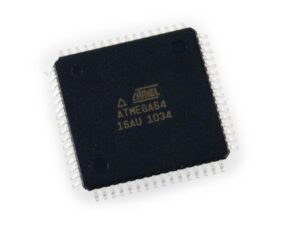
AVR MCU ATMEGA64 Flash Firmware Cloning is a process to attack encrypted atmega64 chip flash memory and readout embedded firmware from atmega64 mcu
The Oscillator can operate in three different modes, each optimized for a specific frequency range. The operating mode is selected by the fuses CKSEL3..1. These options should only be used when not operating close to the maximum frequency of the device, and only if frequency stability at start-up is not important for the application to copy atmega64l chip eeprom memory content. These options are not suitable for crystals.
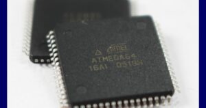
AVR MCU ATMEGA64 flash firmware clonación es un proceso para atacar cifrado atmega64 chip de memoria flash y lectura de firmware embebido de atmega64 mcu;
These options are intended for use with ceramic resonators and will ensure frequency stability at start-up. They can also be used with crystals when not operating close to the maximum frequency of the device, and if frequency stability at start-up is not important for the application.
To use a 32.768kHz watch crystal as the clock source for the device, the Low-frequency Crystal Oscillator must be selected by setting the CKSEL Fuses to “1001”. The crystal should be connected as shown in Figure 11 on page 27. By programming the CKOPT Fuse, the user can enable internal capacitors on XTAL1 and XTAL2 to recover atmega64l mcu flash binary file, thereby removing the need for external capac- itors. The internal capacitors have a nominal value of 36pF.
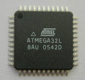
 Reverse Engineer AVR Chip ATMEGA32L Microcontroller
Reverse Engineer AVR Chip ATMEGA32L Microcontroller flash memory protection system is a process to crack mcu atmega32l flash memory fuse bit and readout heximal software from atmega32l mcu flash memory;
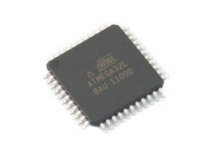
Reverse Engineer AVR Chip ATMEGA32L Microcontroller flash memory protection system is a process to crack mcu atmega32l flash memory fuse bit and readout heximal software from atmega32l mcu flash memory
XTAL1 and XTAL2 are input and output, respectively, of an inverting amplifier which can be con- figured for use as an On-chip Oscillator, as shown in Figure 11. Either a quartz crystal or a ceramic resonator may be used. The CKOPT Fuse selects between two different Oscillator amplifier modes.
When CKOPT is programmed, the Oscillator output will oscillate a full rail-to- rail swing on the output. This mode is suitable when operating in a very noisy environment or when the output from XTAL2 drives a second clock buffer to restore atmega32l mcu flash memory code. This mode has a wide frequency range. When CKOPT is unprogrammed, the Oscillator has a smaller output swing.
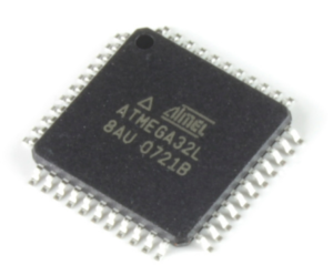
ingeniería inversa AVR chip ATMEGA32L microcontrolador sistema de protección de memoria flash es un proceso para romper mcu atmega32l memoria flash fusible bit y lectura de software heximal de atmega32l mcu memoria flash;
This reduces power consumption considerably. This mode has a limited frequency range and it cannot be used to drive other clock buffers. For resonators, the maximum frequency is 8MHz with CKOPT unprogrammed and 16MHz with CKOPT programmed. C1 and C2 should always be equal for both crystals and resonators.
The optimal value of the capacitors depends on the crystal or resonator in use, the amount of stray capacitance, and the electromagnetic noise of the environment to break atmega32l mcu encryption fuse bit. Some initial guidelines for choosing capacitors for use with crystals are given in Table 4. For ceramic resonators, the capacitor values given by the manufacturer should be used.
 Reverse ATMEL AVR MCU ATmega32A Heximal Code
Reverse ATMEL AVR MCU ATmega32A Heximal Code is a process to unlock atmega32a locked microcontroller fuse bit and read embedded firmware out from atmega32a avr chip flash memory;
The AVR Stack Pointer is implemented as two 8-bit registers in the I/O space. The number of bits actually used is implementation dependent. Note that the data space in some implementations of the AVR architecture is so small that only SPL is needed. In this case, the SPH Register will not be present.
This section describes the general access timing concepts for instruction execution. The Atmel®AVR® CPU is driven by the CPU clock clkCPU, directly generated from the selected clock source for the chip. No internal clock division is used.
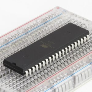
revertir ATMEL AVR MCU ATmega32A código heximal es un proceso para desbloquear atmega32a microcontrolador bloqueado bit fusible y leer el firmware embebido a cabo a partir de atmega32a avr chip de memoria flash
Figure 5 shows the parallel instruction fetches and instruction executions enabled by the Harvard architecture and the fast-access Register File concept. This is the basic pipe-lining concept to obtain up to 1 MIPS per MHz with the corresponding unique results for functions per cost, functions per clocks, and functions per power-unit to copy avr mcu atmega32a software.
Figure 6 shows the internal timing concept for the Register File. In a single clock cycle an ALU operation using two register operands is executed, and the result is stored back to the destination register.
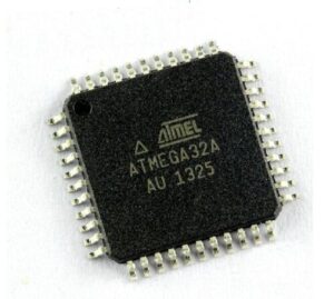
Reverse ATMEL AVR MCU ATmega32A Heximal Code is a process to unlock atmega32a locked microcontroller fuse bit and read embedded firmware out from atmega32a avr chip flash memory
The Atmel®AVR® provides several different interrupt sources. These interrupts and the separate Reset Vector each have a separate Program Vector in the Program memory space. All interrupts are assigned individual enable bits which must be written logic one together with the Global Interrupt Enable bit in the Status Register in order to enable the interrupt by breaking of avr microcontroller atmega32a protection fuse bit.
Depending on the Program Counter value, interrupts may be automatically disabled when Boot Lock Bits BLB02 or BLB12 are programmed. This feature improves software security. See the section “Memory Programming” on page 215 for details.
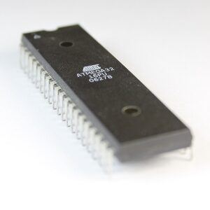
 ATMEL AVR Microcontroller ATmega32 Flash Memory Breaking
ATMEL AVR Microcontroller ATmega32 Flash Memory Breaking is a process to clone embedded code from atmega32 mcu flash memory, the firmware of flash memory of avr mcu atmega32 can be readout;
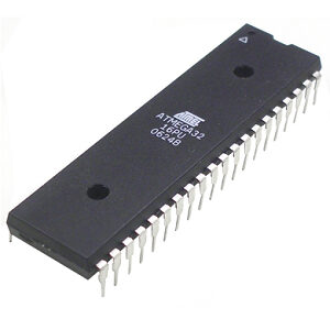
ATMEL AVR Microcontroller ATmega32 Flash Memory Breaking is a process to clone embedded code from atmega32 mcu flash memory, the firmware of flash memory of avr mcu atmega32 can be readout
The Register File is optimized for the AVR Enhanced RISC instruction set. In order to achieve the required performance and flexibility, the following input/output schemes are supported by the Register File:
- One 8-bit output operand and one 8-bit result input
- Two 8-bit output operands and one 8-bit result input
- Two 8-bit output operands and one 16-bit result input
- One 16-bit output operand and one 16-bit result input
Figure 3 shows the structure of the 32 general purpose working registers in the CPU.
Most of the instructions operating on the Register File have direct access to all registers, and most of them are single cycle instructions.
ATMEL AVR microcontrolador ATmega32 romper la memoria flash es un proceso para clonar código embebido de la memoria flash mcu atmega32, el firmware de la memoria flash de avr mcu atmega32 puede ser readout;
As shown in Figure 3, each register is also assigned a Data memory address, mapping them directly into the first 32 locations of the user Data Space. Although not being physically implemented as SRAM locations, this memory organization provides great flexibility in access of the registers to copy avr microcontroller atmega32 flash software, as the X-pointer, Y-pointer, and Z-pointer Registers can be set to index any register in the file.
The registers R26..R31 have some added functions to their general purpose usage. These reg- isters are 16-bit address pointers for indirect addressing of the Data Space. The three indirect address registers X, Y and Z are defined as described in Figure 4.
The Stack is mainly used for storing temporary data, for storing local variables and for storing return addresses after interrupts and subroutine calls. The Stack Pointer Register always points to the top of the Stack. Note that the Stack is implemented as growing from higher memory loca- tions to lower memory locations. This implies that a Stack PUSH command decreases the Stack Pointer.

crack avr atmel microprocessor atmega32 fuse bit and extract embedded code from atmega32 mcu flash memory
The Stack Pointer points to the data SRAM Stack area where the Subroutine and Interrupt Stacks are located. This Stack space in the data SRAM must be defined by the program before any subroutine calls are executed or interrupts are enabled. The Stack Pointer must be set to point above 0x60 by recovering atmega32 microprocessor flash memory content.
The Stack Pointer is decremented by one when data is pushed onto the Stack with the PUSH instruction, and it is decremented by two when the return address is pushed onto the Stack with subroutine call or interrupt. The Stack Pointer is incremented by one when data is popped from the Stack with the POP instruction, and it is incremented by two when address is popped from the Stack with return from subroutine RET or return from interrupt RETI.
