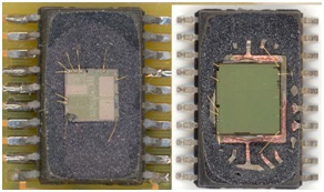
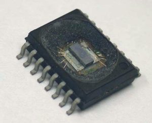
 Recover Chip PIC16F620A Binary
We can Recover Chip PIC16F620A Binary, please view the Chip PIC16F620A features for your reference:
Family and Upward Compatibility
Those users familiar with the PIC16C5X family of microcontrollers will realize that this is an enhanced version of the PIC16C5X architecture. Please refer to Appendix A for a detailed list of enhancements. Code written for the PIC16C5X can be easily ported to PIC16C62X family of devices (Appendix B).
The PIC16C62X family fills the niche for users wanting to migrate up from the PIC16C5X family and not needing various peripheral features of other members of the PIC16XX mid-range microcontroller family when Crack MCU.
Development Support
The PIC16C62X family is supported by a full-featured macro assembler, a software simulator, an in-circuit emulator, a low-cost development programmer and a full-featured programmer which can be usd to Attack Microchip Microcontroller IC Chip Source Code. A “C” compiler and fuzzy logic support tools are also available.
PIC16C62X DEVICE VARIETIES
A variety of frequency ranges and packaging options are available. Depending on application and production requirements the proper device option can be selected using the information in the PIC16C62X Product Identification System section at the end of this data sheet which is important for Attack Microchip IC MCU Encrypted Code.
When placing orders, please use this page of the data sheet to specify the correct part number from Recover Chip PIC16F620A Binary.
Circuit Engineering Company Limited continues to be recognized as the Southern China Leader in Services for IC Read, MCU Recover, Chip Extract, Microcontroller Reverse engineering service.
With the advancement of today’s modern circuit board technology, it is more important than ever to have specialists available to help you at a moment’s notice.
Our engineering and commercial teams collectively have a vast amount of electronic experience covering field include Consumer Electronics, Industrial Automation Electronics, Wireless Communication Electronics., etc. For more information please contact us through email.
Reverse Engineering Microcontroller PIC16C622 Program
PIC16C62X devices have special features to reduce external components, thus reducing system cost, enhancing system reliability and reducing power consumption to Reverse Engineering Microcontroller PIC16C622 Program. There are four oscillator options, of which the single pin RC oscillator provides a low-cost solution, the LP oscillator minimizes power consumption, XT is a standard crystal, and the HS is for High Speed crystals.
The SLEEP (power-down) mode offers power savings. The user can wake up the chip from SLEEP through several external and internal interrupts and reset.
A highly reliable Watchdog Timer with its own on-chip RC oscillator provides protection against software lock- up.
A UV-erasable CERDIP-packaged version is ideal for code development while the cost-effective One-Time Programmable (OTP) version is suitable for production in any volume.
Table 1-1 shows the features of the PIC16C62X mid-range microcontroller families.
A simplified block diagram of the PIC16C62X is shown in below Figure.
Reverse Engineering Microcontroller PIC16C622 Program
The PIC16C62X series fit perfectly in applications ranging from battery chargers to low-power remote sensors. The EPROM technology makes customization of application programs (detection levels, pulse generation, timers, etc.) extremely fast and convenient. The small footprint packages make this microcontroller series perfect for all applications with space limitations. Low-cost, low-power, high-performance, ease of use and I/O flexibility make the PIC16C62X very versatile from Reverse Engineering Microcontroller PIC16C622 Program.
Circuit Engineering Company Limited continues to be recognized as the Southern China Leader in Services for IC Read, MCU Reverse engineering, Chip Extract, Microcontroller Unlock service. With the advancement of today’s modern circuit board technology, it is more important than ever to have specialists available to help you at a moment’s notice. Our engineering and commercial teams collectively have a vast amount of electronic experience covering field include Consumer Electronics, Industrial Automation Electronics, Wireless Communication Electronics., etc. For more information please contact us through email.
Recover Chip PIC16C621 Program
We can Recover Chip PIC16C621 Program, please view the Chip PIC16C621 features for your reference:
Special Microcontroller Features (cont’d)
Programmable code protection
Power saving SLEEP mode
Selectable oscillator options
Serial in-circuit programming (via two pins)
Four user programmable ID locations
CMOS Technology:
· Low-power, high-speed CMOS EPROM technology
· Fully static design
· Wide operating voltage range
– PIC16C62X – 2.5V to 6.0V
– PIC16C62XA – 2.5V to 5.5V
– PIC16CR620A – 2.0V to 5.5V
· Commercial, industrial and extended temperature range
· Low power consumption
– < 2.0 mA @ 5.0V, 4.0 MHz
– 15 µA typical @ 3.0V, 32 kHz
– < 1.0 µA typical standby current @ 3.0V
GENERAL DESCRIPTION
The PIC16C62X are 18 and 20 Pin ROM/EPROM-based members of the versatile PICmicro™ family of low-cost, high-performance, CMOS, fully-static, 8-bit microcontrollers. All PICmicro™ microcontrollers employ an advanced RISC architecture.
The PIC16C62X have enhanced core features, eight-level deep stack, and multiple internal and external interrupt sources when Attack MCU PIC16CE625 Program. The separate instruction and data buses of the Harvard architecture allow a 14-bit wide instruction word with the separate 8-bit wide data.
Recover Chip PIC16C621 Program
The two-stage instruction pipeline allows all instructions to execute in a single-cycle, except for program branches (which require two cycles). A total of 35 instructions (reduced instruction set) are available.
Additionally, a large register set gives some of the architectural innovations used to achieve a very high performance.
Reverse Engineering Microcontroller PIC16C620 Code
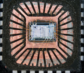
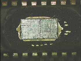
Reverse engineering Microcontroller PIC16C620 Code including the memory content from both eeprom and flash, in order to do that we need to strip off the layer from silicon to metal one and get access to the die finally:
High Performance RISC CPU:
· Only 35 instructions to learn
· All single-cycle instructions (200 ns), except for program branches which are two-cycle
· Operating speed:
– DC – 20 MHz clock input
– DC – 200 ns instruction cycle
Interrupt capability can decide if the difficulty of Recovering Microcontroller PIC16F506 Binary
16 special function hardware registers
8-level deep hardware stack
Direct, Indirect and Relative addressing modes
Reverse Engineering Microcontroller PIC16C620 Code
Peripheral Features:
· 13 I/O pins with individual direction control
· High current sink/source for direct LED drive
· Analog comparator module with:
– Two analog comparators
– Programmable on-chip voltage reference (VREF) module
– Programmable input multiplexing from device inputs and internal voltage reference after Reverse engineering Microcontroller PIC16C620 Code
– Comparator outputs can be output signals
· Timer0: 8-bit timer/counter with 8-bit programmable prescaler
Special Microcontroller Features:
· Power-on Reset (POR)
· Power-up Timer (PWRT) and Oscillator Start-up Timer (OST)
· Brown-out Reset
· Watchdog Timer (WDT) with its own on-chip RC oscillator for reliable operation.
Circuit Engineering Company Limited continues to be recognized as the Southern China Leader in Services for IC Reverse engineering, MCU Crack, Chip Extract, Microcontroller Unlock service.
With the advancement of today’s modern circuit board technology, it is more important than ever to have specialists available to help you at a moment’s notice.
Our engineering and commercial teams collectively have a vast amount of electronic experience covering field include Consumer Electronics, Industrial Automation Electronics, Wireless Communication Electronics., etc. For more information please contact us through email.
Recover Chip PIC16HV785 Hex
Recover Chip PIC16HV785 Hex include the content from both its eeprom and flash, belows we can introduce the program memory organization:
PROGRAM MEMORY ORGANIZATION
The PIC16F785/HV785 has a 13-bit program counter capable of addressing an 8k x 14 program memory space. Only the first 2k x 14 (0000h-07FFh) for the PIC16F785/HV785 is physically implemented. Accessing a location above these boundaries will cause a wrap around within the first 2k x 14 space. The Reset vector is at 0000h and the interrupt vector is at 0004h.
Recover Chip PIC16HV785 Hex
DATA MEMORY ORGANIZATION
The data memory is partitioned into four banks, which contain the General Purpose Registers (GPR) and the Special Function Registers (SFR). The Special Function Registers are located in the first 32 locations of each bank. Register locations 20h-7Fh in Bank 0 and A0h-BFh in Bank 1 are General Purpose Registers, implemented as static RAM.
The last sixteen register locations in Bank 1 (F0h-FFh), Bank 2 (170h-17Fh), and Bank 3 (1F0h-1FFh) point to addresses 70h-7Fh in Bank 0. All other RAM is unimplemented and returns ‘0’ when read.
PROGRAM MEMORY MAP AND STACK FOR THE PIC16F785/HV785
Seven address bits are required to access any location in a data memory bank which can also facilitate the process of IC Cloning. Two additional bits are required to access the four banks. When data memory is accessed directly, the seven Least Significant address bits are contained within the opcode and the two Most Significant bits are contained in the STATUS register for the purpose of recover chip PIC16HV785 Hex.
RP0 and RP1 bits of the STATUS register are the two Most Significant data memory address bits and are also known as the bank select bits. Table 2-1 lists how to access the four banks of registers.
Reverse Engineering Microcontroller PIC16F747 Code
We can Reverse engineering Microcontroller PIC16F747 Code, please view the Microcontroller PIC16F747 features for your reference:
Special Microcontroller Features:
· Fail-Safe Clock Monitor for protecting critical applications against crystal failure when Reverse engineering Microcontroller code;
· Two-Speed Start-up mode for immediate code execution
· Power-on Reset (POR), Power-up Timer (PWRT) and Oscillator Start-up Timer (OST)
· Programmable Code Protection can be used also for Break Microcontroller PIC18F4220 Binary
· Processor Read Access to Program Memory
· Power-Saving Sleep mode
· In-Circuit Serial Programming (ICSP) via two pins
· MPLAB® In-Circuit Debug (ICD) via two pins
· MCLR pin function replaceable with input only pin
DEVICE OVERVIEW
This document contains device specific information about the following devices:
PIC16F737/767 devices are available only in 28-pin packages, while PIC16F747 devices are available in 40-pin and 44-pin packages. All devices in the PIC16F7X7 family share common architecture with the following differences:
· The PIC16F737 and PIC16F767 have one-half of the total on-chip memory of the PIC16F747 and PIC16F777.
· The 28-pin devices have 3 I/O ports, while the 40/44-pin devices have 5.
· The 28-pin devices have 16 interrupts, while the 40/44-pin devices have 17.
· The 28-pin devices have 11 A/D input channels, while the 40/44-pin devices have 14.
· The Parallel Slave Port is implemented only on the 40/44-pin devices.
· Low-Power modes: RC_RUN allows the core and peripherals to be clocked from the INTRC, while SEC_RUN allows the core and peripherals to be clocked from the low-power Timer1. Refer to Section 4.7 “Power-Managed Modes” for further details for the purpose of Reverse engineering Microcontroller code.
Reverse Engineering Microcontroller PIC16F747 Code
· Internal RC oscillator with eight selectable frequencies, including 31.25 kHz, 125 kHz, 250 kHz, 500 kHz, 1 MHz, 2 MHz, 4 MHz and 8 MHz. The INTRC can be configured as a primary or secondary clock source when Crack MCU. Refer to Section 4.5 “Internal Oscillator Block” for further details.
Break IC PIC12F635 Program
We can break IC PIC12F635 Program, please view the PIC12F635 features for your reference:
High-Performance RISC CPU:
· Only 35 instructions to learn:
– All single-cycle instructions except branches
· Operating speed:
– DC – 20 MHz oscillator/clock input
– DC – 200 ns instruction cycle
· Interrupt capability
· 8-level deep hardware stack
· Direct, Indirect and Relative Addressing modes
Special Microcontroller Features:
· Precision Internal Oscillator:
– Factory calibrated to ±1%
– Software selectable frequency range of 8 MHz to 31 kHz
– Software tunable
– Two-Speed Start-up mode
– Crystal fail detect for critical applications
· Clock mode switching for low power operation
· Power-saving Sleep mode
· Wide operating voltage range (2.0V-5.5V)
· Industrial and Extended Temperature range
· Power-on Reset (POR)
· Wake-up Reset (WUR)
Break IC PIC12F635 Program
· Independent weak pull-up/pull-down resistors
· Programmable Low-Voltage Detect (PLVD)
· Power-up Timer (PWRT) and Oscillator Start-up Timer (OST)
· Brown-out Detect (BOD) with software control option
· Enhanced Low-Current Watchdog Timer (WDT) with on-chip oscillator (software selectable nominal 268 seconds with full prescaler) with software enable
· Multiplexed Master Clear with pull-up/input pin
· Programmable code protection (program and data independent)
· High-Endurance Flash/EEPROM cell to crack MCU
– 100,000 write Flash endurance
– 1,000,000 write EEPROM endurance
– Flash/Data EEPROM Retention: > 40 years for the purpose of break IC PIC12F635 Program
Low Power Features:
· Standby Current:
– 1 nA @ 2.0V, typical
· Operating Current:
– 8.5 ìA @ 32 kHz, 2.0V, typical
– 100 ìA @ 1 MHz, 2.0V, typical
· Watchdog Timer Current:
– 1 ìA @ 2.0V, typical
Break IC PIC12F609 Flash Heximal
Break IC PIC12F609 Flash Heximal means the flash memory will have to set up as unlock status, in order to do that we must have an clear idea about its organization:
Program Memory Organization
The PIC12F609 has a 13-bit program counter capable of addressing an 8K x 14 program memory space. Only the first 1K x 14 (0000h-03FFh) for the PIC12F609 is physically implemented. Accessing a location above these boundaries will cause a wraparound within the first 1K x 14 space. The Reset vector is at 0000h and the interrupt vector is at 0004h.
Break IC PIC12F609 Flash Heximal
Data Memory Organization
The data memory (see Figure 2-2) is partitioned into two banks, which contain the General Purpose Registers (GPR) and the Special Function Registers (SFR). The Special Function Registers are located in the first 32 locations of each bank. Register locations 40h-7Fh in Bank 0 are General Purpose Registers, implemented as static RAM. Register locations F0h-FFh in Bank 1 point to addresses 70h-7Fh in Bank 0. All other RAM is unimplemented and returns ‘0’ when read. The RP0 bit of the STATUS register is the bank select bit.
The Special Function Registers are registers used by the CPU and peripheral functions for controlling the desired operation of the device. These registers are static RAM which can be manipulated by Recover MCU PIC16F877 Program.
The special registers can be classified into two sets: core and peripheral. The Special Function Registers associated with the “core” are described in this section. Those related to the operation of the peripheral features are described in the section of that peripheral feature.
The STATUS register, shown in Register 2-1, contains:
· the arithmetic status of the ALU
· the Reset status
· the bank select bits for data memory (RAM)
The STATUS register can be the destination for any instruction, like any other register. If the STATUS register is the destination for an instruction that affects the Z, DC or C bits, then the write to these three bits is disabled. These bits are set or cleared according to the device logic in order to Break IC PIC16F876A Binary. Furthermore, the TO and PD bits are not writable. Therefore, the result of an instruction with the STATUS register as destination may be different than intended for the purpose of Break IC PIC12F609 Flash Heximal.
Break IC PIC16F616 Heximal
Break IC PIC16F616 Heximal starts from get some knowledge about its structure:
PIC16F616/16HV616 only:
· A/D Converter:
– 10-bit resolution
– 8 external input channels
– 2 internal reference channels
· Timer2: 8-bit timer/counter with 8-bit period register, prescaler and postscaler
· Enhanced Capture, Compare, PWM module:
– 16-bit Capture, max. resolution 12.5 ns
– 16-bit Compare, max. resolution 200 ns
– 10-bit PWM with 1, 2 or 4 output channels, programmable “dead time”, max. frequency 20 kHz
Program Memory Organization of PIC16F616/16HV616
The PIC16F610/616/16HV610/616 has a 13-bit program counter capable of addressing an 8k x 14 program memory space. Only the first 1K x 14 (0000h-3FF) for the PIC16F610/16HV610 and the first 2K x 14 (0000h-07FFh) for the PIC16F616/16HV616 is physically implemented to facilitate the process of Recover MCU PIC16F648A Firmware.
Accessing a location above these boundaries will cause a wraparound within the first 1K x 14 space (PIC16F610/16HV610) and 2K x 14 space (PIC16F616/16HV616). The Reset vector is at 0000h and the interrupt vector is at 0004h to ease the process of MCU Cracking.
The data memory (see Figure 2-4) is partitioned into two banks, which contain the General Purpose Registers (GPR) and the Special Function Registers (SFR). The Special Function Registers are located in the first 32 locations of each bank.
Break IC PIC16F616 Heximal
PIC16F610/16HV610 Register locations 40h-7Fh in Bank 0 are General Purpose Registers, implemented PC gram counter capable of addressing an 8k x 14 program memory space. Only the first 1K x 14 (0000h-3FF) for the PIC16F610/16HV610 and the first 2K x 14 (0000h-07FFh) for the PIC16F616/16HV616 is physically implemented to facilitate the process of Copy Microcontroller PIC16F737 Flash.
Accessing a location above these boundaries will cause a wraparound within the first 1K x 14 space (PIC16F610/16HV610) and 2K x 14 space (PIC16F616/16HV616). The Reset vector is at 0000h and the interrupt vector is at 0004h after Break IC PIC16F616 Heximal
Break IC PIC16F610 Binary
We can break IC PIC16F610 Binary, please view the Microchip IC PIC16F610 features for your reference:
High-Performance RISC CPU:
· Only 35 instructions to learn:
– All single-cycle instructions except branches
· Operating speed:
– DC – 20 MHz oscillator/clock input
– DC – 200 ns instruction cycle
· Interrupt capability
· 8-level deep hardware stack
· Direct, Indirect and Relative Addressing modes
Break IC PIC16F610 Binary
Special Microcontroller Features:
· Precision Internal Oscillator:
– Factory calibrated to ±1%, typical
– User selectable frequency: 4 MHz or 8 MHz
· Power-Saving Sleep mode
· Voltage range:
– PIC16F610/616: 2.0V to 5.5V
– PIC16HV610/616: 2.0V to user defined maximum (see note)
· Industrial and Extended Temperature range
· Power-on Reset (POR)
· Power-up Timer (PWRT) and Oscillator Start-up Timer (OST)
· Brown-out Reset (BOR)
· Watchdog Timer (WDT) with independent oscillator for reliable operation only after the process of Attack MCU PIC12F675 Binary has been completed.
· Multiplexed Master Clear with pull-up/input pin
· Programmable code protection
· High Endurance Flash:
– 100,000 write Flash endurance
– Flash retention: > 40 years for the purpose of break IC PIC16F610 Binary
Low-Power Features:
· Standby Current:
– 50 nA @ 2.0V, typical
· Operating Current:
– 20 ìA @ 32 kHz, 2.0V, typical
– 220 ìA @ 4 MHz, 2.0V, typical
· Watchdog Timer Current:
– 1 ìA @ 2.0V, typical
Peripheral Features:
· Shunt Voltage Regulator (PIC16HV610/616 only):
– 5 volt regulation
– 4 mA to 50 mA shunt range
· 11 I/O pins and 1 input only
– High current source/sink for direct LED drive
– Interrupt-on-Change pins
– Individually programmable weak pull-ups
· Analog Comparator module with:
– Two analog comparators
– Programmable on-chip voltage reference (CVREF) module (% of VDD)
– Fixed Voltage Reference
– Comparator inputs and outputs externally accessible
– SR Latch
– Built-In Hysteresis (user selectable)
· Timer0: 8-bit timer/counter with 8-bit programmable prescaler
· Enhanced Timer1:
– 16-bit timer/counter with prescaler
– External Timer1 Gate (count enable)
– Option to use OSC1 and OSC2 in LP mode as Timer1 oscillator if INTOSC mode selected
– Timer1 oscillator
· In-Circuit Serial ProgrammingTM (ICSPTM) via two pins