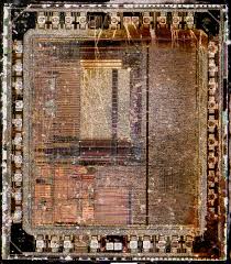
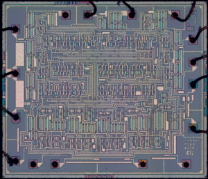
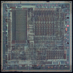
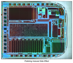
 Break IC TS83C51U2 Heximal
Break IC TS83C51U2 Heximal
We can Break IC TS83C51U2 Heximal, please view the IC TS83C51U2 features for your reference:
In this document, UART_0 will make reference to the first UART (present in all Atmel Wireless & Microcontrollers C51 derivatives) and UART_1 will make reference to the second UART, only present in the TS80C51U2 part.
The second UART (UART_1) can be seen as an alternate function of Port 1 (P1.2 or P1.6 for RXD1 and P1.3 or P1.7 for TXD1) or can be connected to (pin6 or pin12) and (pin28 or pin34) of 44-pin package (see Pin configuration). UART_1 is fully compliant with the first one allowing an internal baud rate generator to be the clock source.
This common internal baud rate generator can be used independently by each UART or both as clock source allowing to program various speeds.
The TS80C51U2 provides 7 sources of interrupt with four priority levels. UART_1 has a lower priority than Timer
The Serial Ports are full duplex meaning they can transmit and receive simultaneously. They are also receive buffered, meaning they can start reception of a second byte before a previously received byte has been break from the receive register from Break IC TS83C51U2 Heximal.
The Serial Port receive and transmit registers of UART_1 are both accessed at Special Function Register SBUF_1. Writing to SBUF_1 loads the transmit register and breaking SBUF_1 accesses a physical separate receive register.
Break IC TS83C51U2 Heximal
The UART_1 port control and status is the Special Function Register SCON_1. This register contains not only the mode selection bit but also the 9th bit for transmit and receive (TB8_1 and RB8_1) and the serial port interrupt bits (TI_1 and RI_1).
The automatic address recognition feature is enabled when multiprocessor communication is enabled. Implemented in hardware, automatic address recognition enhances the multiprocessor communication feature by allowing the Serial Port to examine address of each incoming frame and provides filtering capability after Break IC TS83C51U2 Heximal.
The UART_1 also comes with Frame error detection, similar to the UART_0. The Special Function Registers (SFRs) of the TS80C51U2 fall into the following categories:
C51 core registers: ACC, B, DPH, DPL, PSW, SP, AUXR1
I/O port registers: P0, P1, P2, P3 after Break IC
Timer registers: T2CON, T2MOD, TCON, TH0, TH1, TH2, TMOD, TL0, TL1, TL2, RCAP2L, RCAP2H
Serial I/O port registers for UART_0: SADDR_0, SADEN_0, SBUF_0, SCON_0
Serial I/O port registers for UART_1: SADDR_1, SADEN_1, SBUF_1, SCON_1
Baud Rate Generator registers: BRL, BDRCON, BDRCON_1
Power and clock control registers: PCON
HDW Watchdog Timer Reset: WDTRST, WDTPRG
Interrupt system registers: IE, IP, IPH
Others: AUXR, CKCONIn comparison to the original 80C52, the TS80C51U2 implements some new features, which are:
The X2 option
The second full duplex enhanced UART.
The Baud Rate generator.
The Dual Data Pointer.
The Watchdog.
The 4 level interrupt priority system.
The power-off flag.
The ONCE mode.
The ALE disabling.
Some enhanced features are also located in the UARTs and the timer 2
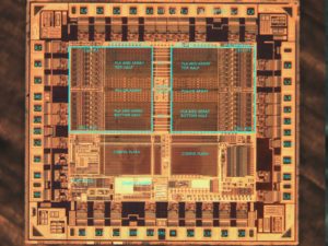
Break IC TS83C51U2 Binary
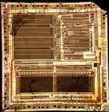
We can Break IC TS83C51U2 Binary, please view the IC TS83C51U2 features for your reference:
In this document, UART_0 will make reference to the first UART (present in all Atmel Wireless & Microcontrollers C51 derivatives) and UART_1 will make reference to the second UART, only present in the TS80C51U2 part. The second UART (UART_1) can be seen as an alternate function of Port 1 (P1.2 or P1.6 for RXD1 and P1.3 or P1.7 for TXD1) or can be connected to (pin6 or pin12) and (pin28 or pin34) of 44-pin package (see Pin configuration). UART_1 is fully compliant with the first one allowing an internal baud rate generator to be the clock source if Break IC.
This common internal baud rate generator can be used independently by each UART or both as clock source allowing to program various speeds.The TS80C51U2 provides 7 sources of interrupt with four priority levels. UART_1 has a lower priority than Timer, The Serial Ports are full duplex meaning they can transmit and receive simultaneously.
They are also receive buffered, meaning they can start reception of a second byte before a previously received byte has been break from the receive register.
The Serial Port receive and transmit registers of UART_1 are both accessed at Special Function Register SBUF_1. Writing to SBUF_1 loads the transmit register and breaking SBUF_1 accesses a physical separate receive register.
The UART_1 port control and status is the Special Function Register SCON_1. This register contains not only the mode selection bit but also the 9th bit for transmit and receive (TB8_1 and RB8_1) and the serial port interrupt bits (TI_1 and RI_1) before Break IC TS83C51U2 Binary.
Break IC TS83C51U2 Binary
The automatic address recognition feature is enabled when multiprocessor communication is enabled. Implemented in hardware, automatic address recognition enhances the multiprocessor communication feature by allowing the Serial Port to examine address of each incoming frame and provides filtering capability.
The UART_1 also comes with Frame error detection, similar to the UART_0. The Special Function Registers (SFRs) of the TS80C51U2 fall into the following categories:
C51 core registers: ACC, B, DPH, DPL, PSW, SP, AUXR1
I/O port registers: P0, P1, P2, P3 after Break IC
Timer registers: T2CON, T2MOD, TCON, TH0, TH1, TH2, TMOD, TL0, TL1, TL2, RCAP2L, RCAP2H
Serial I/O port registers for UART_0: SADDR_0, SADEN_0, SBUF_0, SCON_0
Serial I/O port registers for UART_1: SADDR_1, SADEN_1, SBUF_1, SCON_1
Baud Rate Generator registers: BRL, BDRCON, BDRCON_1
Power and clock control registers: PCON
HDW Watchdog Timer Reset: WDTRST, WDTPRG
Interrupt system registers: IE, IP, IPH
Others: AUXR, CKCONIn comparison to the original 80C52, the TS80C51U2 implements some new features, which are:
The X2 option
The second full duplex enhanced UART.
The Baud Rate generator.
The Dual Data Pointer.
The Watchdog.
The 4 level interrupt priority system.
The power-off flag.
The ONCE mode.
The ALE disabling.
Some enhanced features are also located in the UARTs and the timer 2.
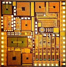
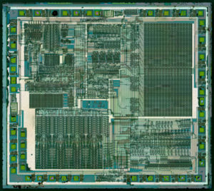
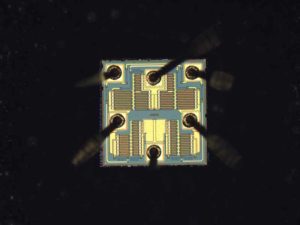
Recover Mcu TS80C51U2 Flash
Recover Mcu TS80C51U2 Flash
Recover Mcu TS80C51U2 Flash
We can Recover Mcu TS80C51U2 Flash, please view the Mcu TS80C51U2 features for your reference:
TS80C51U2 is high performance CMOS ROM, OTP and EPROM versions of the 80C51 CMOS single mcu 8-bit microcontroller. The TS80C51U2 retains all features of the 80C51 with extended ROM/EPROM capacity (16 Kbytes), 256 bytes of internal RAM, a 7-source , 4-level interrupt system, an on-mcu oscilator and three timer/counters. In addition, the TS80C51U2 has a second UART, enhanced functions on both UART, enhanced timer 2, a hardware watchdog timer, a dual data pointer, a baud rate generator and a X2 speed improvement mechanism. The fully static design of the TS80C51U2 allows to reduce system power consumption by bringing the clock frequency down to any value, even DC, without loss of data.
The TS80C51U2 has 2 software-selectable modes of reduced activity for further reduction in power consumption. In the idle mode the CPU is frozen while the timers, the serial port and the interrupt system are still operating. In the power-down mode the RAM is saved and all other functions are inoperative.
80C52 Compatible
8051 pin and instruction compatible
Four 8-bit I/O ports
Three 16-bit timer/counters
256 bytes scratchpad RAM
High-Speed Architecture
40 MHz @ 5V, 30MHz @ 3V
X2 Speed Improvement capability (6 clocks/machine cycle)
Recover Mcu TS80C51U2 Flash
30 MHz @ 5V, 20 MHz @ 3V (Equivalent to 60 MHz @ 5V, 40 MHz @ 3V) before Recover Mcu TS80C51U2 Flash
Second UART
Baud Rate Generator
Dual Data Pointer
On-mcu ROM/EPROM (16K-bytes)
Programmable Clock Out and Up/Down Timer/ Counter 2
Hardware Watchdog Timer (One-time enabled with Reset-Out)
Asynchronous port reset
Interrupt Structure with
7 Interrupt sources
4 level priority interrupt system
Full duplex Enhanced UARTs
Framing error detection
Automatic address recognition
Low EMI (inhibit ALE)
Power Control modes after Recover Mcu
Idle mode
Power-down mode
Power-off Flag
Once mode (On-mcu Emulation)
Power supply: 4.5-5.5V, 2.7-5.5V
Temperature ranges: Commercial (0 to 70oC) and
Industrial (-40 to 85oC)
Packages: PDIL40, PLCC44, VQFP44 1.4, CQPJ44 (window), CDIL40 (window)
Break MCU AT87LV51 Software
We can Break MCU AT87LV51 Software, please view the Mcu AT87LV51 features for your reference:
The AT87LV51 is a low-voltage, high-performance CMOS 8-bit mcu with 4K bytes of QuickFlash One-Time Programmable (OTP) memory when Recover MCU Microchip CF755 Dump. The device is manufactured using Atmel’s high-density nonvolatile memory technology and is compatible with the industry standard MCS-51 instruction set and pinout.
The on-chip QuickFlash allows the program memory to be user programmed by a conventional nonvolatile memory programmer. By combining a versatile 8-bit CPU with QuickFlash on a monolithic chip, the Atmel AT87LV51 is a powerful mcu that provides a highly flexible and cost-effective solution to many embedded control applications.
The AT87LV51 provides the following standard features: 4K bytes of QuickFlash OTP program memory, 128 bytes of RAM, 32 I/O lines, two 16-bit timer/counters, a five-vector, 2-level interrupt architecture, a full duplex serial port, on-chip oscillator, and clock circuitry. In addition, the AT87LV51 is designed with static logic for operation down to zero frequency and supports two software-selectable power-saving modes after Break MCU AT87LV51 Software.
The Idle mode stops the CPU while allowing the RAM, timer/counters, serial port and interrupt system to continue functioning. The Power-down mode saves the RAM contents but freezes the oscillator disabling all other chip functions until the next hardware reset. XTAL1 and XTAL2 are the input and output, respectively, of an inverting amplifier, which can be configured for use as an on-chip oscillator.
Either a quartz crystal or ceramic resonator may be used. To drive the device from an external clock source, XTAL2 should be left unconnected while XTAL1 is driven as shown in below Figure. There are no requirements on the duty cycle of the external clock signal, since the input to the internal clocking circuitry is through a divide-by-two flip-flop, but minimum and maximum voltage high and low time specifications must be observed.
Break MCU AT87LV51 Software
In Idle Mode, the CPU puts itself to sleep while all the on chip peripherals remain active. The mode is invoked by software. The content of the on-chip RAM and all the Special Function registers remains unchanged during this mode. The Idle mode can be terminated by any enabled interrupt or by a hardware reset when Break MCU AT87LV51 Software.
It should be noted that when Idle is terminated by a hardware reset, the device normally resumes program execution from where it left off, up to two machine cycles before the internal reset algorithm takes control. On-chip hardware inhibits access to internal RAM in this event to Unlock Microcontroller, but access to the port pins is not inhibited.
To eliminate the possibility of an unexpected write to a port pin when Idle is terminated by reset, the instruction following the one that invokes Idle should not be one that writes to a port pin or to external memory.
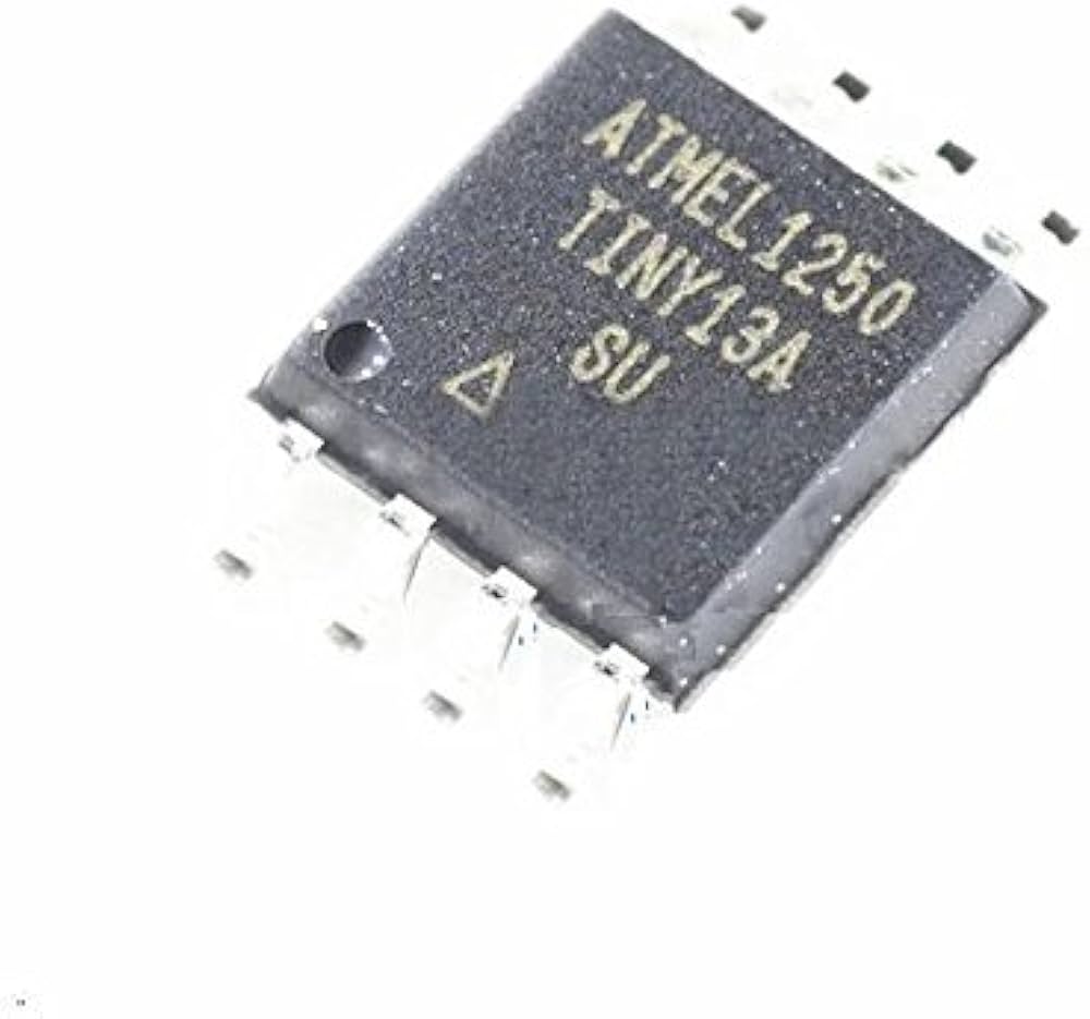
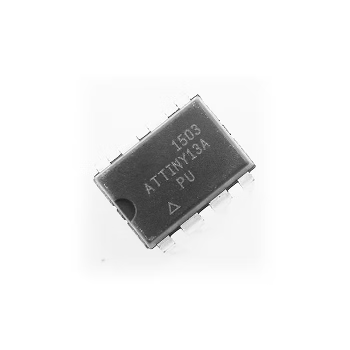
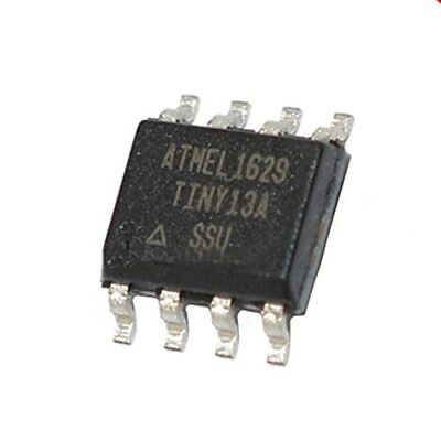
Recover Microcontroller ATtiny13A Heximal
Recovering microcontroller ATtiny13A heximal involves a process of cracking or decoding the secured firmware stored in its flash memory and EEPROM memory of encrypted MCU ATtiny13A. The ATtiny13A, like many microcontrollers (MCUs), may have encrypted or locked firmware to protect its program and source code. However, using reverse engineering techniques, experts can break these ATtiny13A microprocessor’s protective layers and unlock the microprocessor’s memory to retrieve the heximal data.
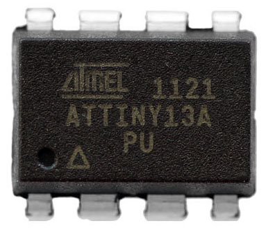
Recovering microcontroller ATtiny13A heximal involves a process of cracking or decoding the secured firmware stored in its flash memory and EEPROM memory of encrypted MCU ATtiny13A. The ATtiny13A, like many microcontrollers (MCUs), may have encrypted or locked firmware to protect its program and source code. However, using reverse engineering techniques, experts can break these ATtiny13A microprocessor’s protective layers and unlock the microprocessor’s memory to retrieve the heximal data.
The recovery process starts by analyzing the microcontroller’s architecture to identify encryption protocols. Once these protections are bypassed, the binary or heximal firmware can be extracted. This data is essential for restoring or replicating the original program, enabling system recovery or hardware duplication.
Decoding or decrypting the ATtiny13A’s firmware allows developers to restore lost data or replicate the software for new devices. However, these actions must be conducted within legal and ethical guidelines to avoid violating intellectual property rights.
The AVR core combines a rich instruction set with 32 general purpose working registers which will provide benefit for Recover Microcontroller ATtiny13A Heximal. All 32 registers are directly connected to the Arithmetic Logic Unit (ALU), allowing two independent registers to be accessed in one single instruction executed in one clock cycle. The resulting architecture is more code efficient while achieving throughputs up to ten times faster than conventional CISC microcontrollers.
The ATtiny13A provides the following features: 1K byte of In-System Programmable Flash, 64 bytes EEPROM, 64 bytes SRAM, 6 general purpose I/O lines, 32 general purpose working registers, one 8-bit Timer/Counter with compare modes, Internal and External Interrupts, a 4-channel, 10-bit ADC, a programmable Watchdog Timer with internal Oscillator, and three software selectable power saving modes if Recover Microcontroller ATTINY13A Heximal.
mbalekake microcontroller ATtiny13A heximal melu proses cracking utawa dekoding perangkat kukuh aman disimpen ing memori lampu kilat lan memori EEPROM saka ndhelik MCU ATtiny13A. ATtiny13A, kaya akeh mikrokontroler (MCU), bisa uga duwe perangkat kukuh sing dienkripsi utawa dikunci kanggo nglindhungi program lan kode sumber. Nanging, kanthi nggunakake teknik rekayasa terbalik, para ahli bisa ngilangi lapisan pelindung mikroprosesor ATtiny13A iki lan mbukak kunci memori mikroprosesor kanggo njupuk data heksimal.
The Idle mode stops the CPU while allowing the SRAM, Timer/Counter, ADC, Analog Comparator, and Interrupt system to continue functioning. The Power-down mode saves the register contents, disabling all chip functions until the next Interrupt or Hardware Reset. The ADC Noise Reduction mode stops the CPU and all I/O modules except ADC, to minimize switching noise during ADC conversions.
The device is manufactured using Atmel’s high density non-volatile memory technology. The On-chip ISP Flash allows the Program memory to be re-programmed In-System through an SPI serial interface, by a conventional non-volatile memory programmer or by an On-chip boot code running on the AVR core.
The ATtiny13A AVR is supported with a full suite of program and system development tools including: C Compilers, Macro Assemblers, Program Debugger/Simulators, and Evaluation kits if Recover MICROCONTROLLER.
మైక్రోకంట్రోలర్ ATtiny13A హెక్సిమల్ని పునరుద్ధరించడం అనేది దాని ఫ్లాష్ మెమరీలో నిల్వ చేయబడిన సురక్షిత ఫర్మ్వేర్ మరియు ఎన్క్రిప్టెడ్ MCU ATtiny13A యొక్క EEPROM మెమరీని క్రాకింగ్ లేదా డీకోడింగ్ చేసే ప్రక్రియను కలిగి ఉంటుంది. ATtiny13A, అనేక మైక్రోకంట్రోలర్ల (MCUలు) వలె, దాని ప్రోగ్రామ్ మరియు సోర్స్ కోడ్ను రక్షించడానికి ఫర్మ్వేర్ను ఎన్క్రిప్ట్ చేసి లేదా లాక్ చేసి ఉండవచ్చు. అయినప్పటికీ, రివర్స్ ఇంజనీరింగ్ పద్ధతులను ఉపయోగించి, నిపుణులు ఈ ATtiny13A మైక్రోప్రాసెసర్ యొక్క రక్షణ పొరలను విచ్ఛిన్నం చేయవచ్చు మరియు హెక్సిమల్ డేటాను తిరిగి పొందడానికి మైక్రోప్రాసెసర్ మెమరీని అన్లాక్ చేయవచ్చు.
For compatibility with future devices, reserved bits should be written to zero if accessed. Reserved I/O memory addresses should never be written when Break IC PIC16F684 Binary.
I/O Registers within the address range 0x00 – 0x1F are directly bit-accessible using the SBI and CBI instructions. In these registers, the value of single bits can be checked by using the SBIS and SBIC instructions.ome of the Status Flags are cleared by writing a logical one to them. Note that, unlike most other AVRs, the CBI and SBI instructions will only operation the specified bit, and can therefore be used on registers containing such Status Flags. The CBI and SBI instructions work with registers 0x00 to 0x1F.
Recover Microcontroller ATtiny13A Heximal
This documentation contains simple code examples that briefly show how to use various parts of the device. These code examples assume that the part specific header file is included before compilation. Be aware that not all C compiler vendors include bit definitions in the header files and interrupt handling in C is compiler dependent. Please confirm with the C compiler documentation for more details.
Die Wiederherstellung des Mikrocontrollers ATtiny13A Heximal umfasst einen Prozess zum Knacken oder Dekodieren der gesicherten Firmware, die im Flash-Speicher und EEPROM-Speicher des verschlüsselten MCU ATtiny13A gespeichert ist. Der ATtiny13A kann, wie viele Mikrocontroller (MCUs), eine verschlüsselte oder gesperrte Firmware haben, um sein Programm und seinen Quellcode zu schützen. Mithilfe von Reverse-Engineering-Techniken können Experten jedoch diese Schutzschichten des ATtiny13A-Mikroprozessors durchbrechen und den Speicher des Mikroprozessors entsperren, um die Heximal-Daten abzurufen.
Recover Microcontroller AT80F51 Eeprom
We can Recover Microcontroller AT80F51 Eeprom, please view the Microcontroller AT80F51 features for your reference:
The AT80F51 is a low-power, high-performance CMOS 8-bit microcomputer with 4K bytes of QuickFlash Memory. The device is manufactured using Atmel’s high density nonvolatile memory technology and is compatible with the industry standard MCS- 51™ instruction set and pinout.
The on-microcontroller QuickFlash allows custom codes to be quickly programmed in the factory. By combining a versatile 8-bit CPU with Quick-Flash on a monolithic microcontroller which carry out the same method as Recover MCU PIC16F876 Binary, the Atmel AT80F51 is a powerful microcomputer which provides a highly flexible and cost effective solution to many embedded control applications.
The AT80F51 provides the following standard features: 4K bytes of QuickFlash, 128 bytes of RAM, 32 I/O lines, two 16-bit timer/counters, a five vector two-level interrupt architecture, a full duplex serial port, on-microcontroller oscillator and clock circuitry. In addition, the AT80F51 is designed with static logic for operation down to zero frequency and supports two software selectable power saving modes through the purpose of Recover MCU PIC16F877 Heximal.
The Idle Mode stops the CPU while allowing the RAM, timer/counters, serial port and interrupt system to continue functioning. The Power Down Mode saves the RAM contents but freezes the oscillator disabling all other microcontroller functions until the next hardware reset.
Recover Microcontroller AT80F51 Eeprom
XTAL1 and XTAL2 are the input and output, respectively, of an inverting amplifier which can be configured for use as an on-microcontroller oscillator, as shown in Figure 1. Either a quartz In idle mode, the CPU puts itself to sleep while all the on- microcontroller peripherals remain active. The mode is invoked by software.
The content of the on-microcontroller RAM and all the special functions registers remain unchanged during this mode. The idle mode can be terminated by any enabled interrupt or by a hardware reset. It should be noted that when idle is terminated by a hardware reset, the device normally resumes program execution when Crack MCU, from where it left off, up to two machine cycles before the internal reset algorithm takes control when Recover Microcontroller AT80F51 Eeprom.
On-microcontroller hardware inhibits access to internal RAM in this event, but access to the port pins is not inhibited. To eliminate the possibility of nated. The only exit from power down is a hardware reset. Reset redefines the SFRs but does not change the on-microcontroller RAM. The reset should not be activated before VCC is restored to its normal operating level and must be held active long enough to allow the oscillator to restart and stabilize.
Recover MCU PIC16HV540 Binary
Recover MCU PIC16HV540 Binary
We can Recover MCU PIC16HV540 Binary, please view the MCU PIC16HV540 features for your reference:
High-Performance RISC CPU:
· Only 33 single word instructions to learn
· All instructions are single cycle (200 ns) except for program branches which are two-cycle
· Operating speed: DC – 20 MHz clock input DC – 200 ns instruction cycle
· 12-bit wide instructions
· 8-bit wide data path
· Seven special function hardware registers
· Four-level deep hardware stack
· Direct, indirect and relative addressing modes for data and instructions to Recover IC program
Peripheral Features:
· 8-bit real time clock/counter (TMR0) with 8-bit programmable prescaler
· Power-On Reset (POR)
· Brown-Out Protection
· Device Reset Timer (DRT) with short RC oscillator start-up time
· Programmable Watchdog Timer (WDT) with its own on-chip RC oscillator for reliable operation
· Sleep Timer
· 8 High Voltage I/O
· 4 Regulated I/O
· Wake up from SLEEP on-pin change
· Programmable code protection
· Power saving SLEEP mode
· Selectable oscillator options:
– RC: Low-cost RC oscillator
– XT: Standard crystal/resonator
– HS: High speed crystal/resonator
– LP: Power saving, low frequency crystal
· Glitch filtering on MCLR and pin change inputs
Recover MCU PIC16HV540 Binary
CMOS Technology:
· Selectable on-chip 3V/5V Regulator
· Low-power, high-speed CMOS EPROM technology for the purpose of Decrypt IC program
· Fully static design
· Wide-operating voltage range:
– 3.5V to 15V
· Temperature range:
– Commercial: 0°C to 70°C
– Industrial: -40°C to 85°C
· Low-power consumption
– < 2 mA typical @ 5V, 4 MHz
– 15 µA typical @ 3V, 32 kHz
– < 4.5 µA typical standby current @ 15V (with WDT disabled), 0°C to 70°C
The PIC16HV540 from Microchip Technology is a low- cost, high-performance, 8-bit, fully-static, EPROM- based CMOS microcontroller. It is pin and software compatible with the PIC16C5X family of devices. It employs a RISC architecture with only 33 single word single cycle instructions when Crack MCU. All instructions are single cycle except for program branches, which take two cycles. The PIC16HV540 delivers performance an order of magnitude higher than its competitors in the same price category after Recover MCU PIC16HV540 Binary.
The 12-bit wide instructions are highly orthogonal resulting in 2:1 code compression over other 8-bit microcontrollers in its class. The easy-to-use and easy-to-remember instruction set reduces development time significantly.
The PIC16HV540 is the first One-Time-Programmable (OTP) microcontroller with an on-chip 3 volt and 5 volt regulator. This eliminates the need for an external regulator in many applications powered from 9 Volt or 12 Volt batteries or unregulated 6 volt, 9 volt or 12 volt mains adapters.
The PIC16HV540 is ideally suited for applications that require very low standby current at high voltages. These typically require expensive low current regulators.
Break MCU PIC12CE674 Software
The high performance of the PIC12CE67X family can be attributed to a number of architectural features commonly found in RISC microprocessors which is critical part for Break MCU PIC12CE674 Software. To begin with, the PIC12CE67X uses a Harvard architecture, in which program and data are accessed from separate memories using separate buses.
This improves bandwidth over traditional von Neumann architecture in which program and data are fetched from the same memory using the same bus. Separating program and data buses also allow instructions to be sized differently than the 8-bit wide data word. Instruction opcodes are 14-bits wide making it possible to have all single word instructions.
A 14-bit wide program memory access bus fetches a 14-bit instruction in a single instruction cycle. A two-stage pipeline overlaps fetch and execution of instructions to facilitate the process of Copy MCU PIC18F4685 Software. Consequently, all instructions (35) execute in a single cycle (400 ns @ 10 MHz) except for program branches.
The table below lists program memory (EPROM), data memory (RAM), and non-volatile memory (EEPROM) for each PIC12C67X device. The PIC12C67X can directly or indirectly address its register files or data memory. All special function registers, including the program counter, are mapped in the data memory after Break MCU PIC12CE674 Software.
The PIC12C67X has an orthogonal (symmetrical) instruction set that makes it possible to carry out any operation on any register using any addressing mode to Crack MCU. This symmetrical nature and lack of ‘special optimal situations’ make programming with the PIC12C67X simple yet efficient.
In addition, the learning curve is reduced significantly. PIC12C67X devices contain an 8-bit ALU and working register. The ALU is a general purpose arithmetic unit. It performs arithmetic and Boolean functions between the data in the working register and any register file.
Break MCU PIC12CE674 Software
The ALU is 8-bits wide and capable of addition, subtraction, shift and logical operations. Unless otherwise mentioned, arithmetic operations are two’s complement in nature. In two-operand instructions, typically one operand is the working register (W register).
The other operand is a file register or an immediate constant. In single operand instructions, the operand is either the W register or a file register only after the completion of Recover IC PIC16F873 Heximal. The W register is an 8-bit working register used for ALU operations. It is not an addressable register.
Depending on the instruction executed, the ALU may affect the values of the Carry (C), Digit Carry (DC), and Zero (Z) bits in the STATUS register. The C and DC bits operate as a borrow bit and a digit borrow out bit, respectively, in subtraction. See the SUBLW and SUBWF instructions for examples.
Break Microcontroller PIC12C672 Heximal
The PIC12C67X devices are low-cost, high-performance, CMOS, fully-static, 8-bit microcontrollers with integrated analog-to-digital (A/D) converter and EEPROM data memory (EEPROM on PIC12CE67X versions only) when Break Microcontroller PIC12C672 Heximal.
All PICmicro® microcontrollers employ an advanced RISC architecture. The PIC12C67X microcontrollers have enhanced core features, eight-level deep stack, and multiple internal and external interrupt sources. The separate instruction and data buses of the Harvard architecture allow a 14-bit wide instruction word with the separate 8-bit wide data after IC Cloning. The two stage instruction pipeline allows all instructions to execute in a single cycle, except for program branches, which require two cycles.
Break Microcontroller PIC12C672 Heximal
A total of 35 instructions (reduced instruction set) are available. Additionally, a large register set gives some of the architectural innovations used to achieve a very high performance. PIC12C67X microcontrollers typically achieve a 2:1 code compression and a 4:1 speed improvement over other 8-bit microcontrollers in their class.
The PIC12C67X devices have 128 bytes of RAM, 16 bytes of EEPROM data memory (PIC12CE67X only), 5 I/O pins and 1 input pin. In addition a timer/counter is available. Also a 4-channel, high-speed, 8-bit A/D is provided. The 8-bit resolution is ideally suited for applications requiring low-cost analog interface which can be used for MC68HC05B6 microcontroller ic extract code, (i.e., thermostat control, pressure sensing, etc.) before Break MICROCONTROLLER
The PIC12C67X devices have special features to reduce external components, thus reducing cost, The PIC12C67X products are compatible with other members of the 14-bit PIC16CXXX families. enhancing system reliability and reducing power consumption.
The Power-On Reset (POR), Power-up Timer (PWRT), and Oscillator Start-up Timer (OST) eliminate the need for external reset circuitry. There are five oscillator configurations to choose from, including INTRC precision internal oscillator mode and the power-saving LP (Low Power) oscillator mode when Extract PIC16F84 MCU firmware. Power-saving SLEEP mode, Watchdog Timer and code protection features improve system cost, power and reliability.
The SLEEP (power-down) feature provides a power-saving mode. The user can wake-up the chip from SLEEP through several external and internal interrupts and resets when Break Microcontroller PIC12C672 Heximal.
Break IC PIC12C671 Eeprom
We can Break IC PIC12C671 Eeprom, please view the IC PIC12C671 features for your reference:
High-Performance RISC CPU:
· Only 35 single word instructions to learn
· All instructions are single cycle (400 ns) except for program branches which are two-cycle
· Operating speed: DC – 10 MHz clock input DC – 400 ns instruction cycle
· 14-bit wide instructions 8-bit wide data path
· Interrupt capability
· Special function hardware registers
· 8-level deep hardware stack
· Direct, indirect and relative addressing modes for data and instructions to facilitate the process of Extract PLD IC Firmware
Peripheral Features:
· Four-channel, 8-bit A/D converter
· 8-bit real time clock/counter (TMR0) with 8-bit programmable prescaler
· 1,000,000 erase/write cycle EEPROM data memory
· EEPROM data retention > 40 years
Special Microcontroller Features:
Break IC PIC12C671 Eeprom
In-Circuit Serial Programming (ICSP™)
Internal 4 MHz oscillator with programmable calibration
Selectable clockout
Power-on Reset (POR)
Power-up Timer (PWRT) and Oscillator Start-up Timer (OST)
Watchdog Timer (WDT) with its own on-chip RC oscillator for reliable operation in order to Extract PLD MCU code
Power saving SLEEP mode
Interrupt-on-pin change (GP0, GP1, GP3)
Internal pull-ups on I/O pins (GP0, GP1, GP3)
Internal pull-up on MCLR pin
Selectable oscillator options:
– INTRC: Precision internal 4 MHz oscillator
– EXTRC: External low-cost RC oscillator
– XT: Standard crystal/resonator
– HS: High speed crystal/resonator after Break IC PIC12C671 Eeprom
– LP: Power saving, low frequency crystal
CMOS Technology:
· Low-power, high-speed CMOS EPROM/EEPROM technology
· Fully static design to against the process of MCU Cracking
· Wide operating voltage range 2.5V to 5.5V
· Commercial, Industrial and Extended temperature ranges
· Low power consumption
< 2 mA @ 5V, 4 MHz
15 µA typical @ 3V, 32 kHz
< 1 µA typical standby current