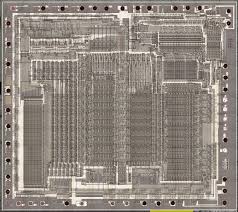
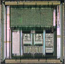
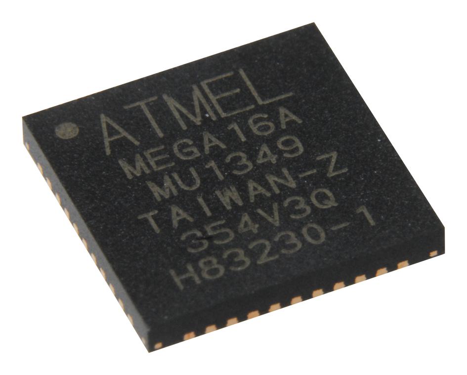
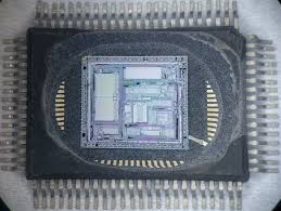
 Break MCU ATmega128PA Firmware
The Atmel® AVR® core combines a rich instruction set with 32 general purpose working registers. All the 32 registers are directly connected to the Arithmetic Logic Unit (ALU) which can provide great support for Break MCU ATmega128PA Firmware, allowing two independent registers to be accessed in one single instruction executed in one clock cycle.
The resulting architecture is more code efficient while achieving throughputs up to ten times faster than conventional CISC microcontrollers in order to Copy IC PIC16F886 Firmware. The ATmega128 provides the following features: 128Kbytes of In-System Programmable Flash with Break-While-Write capabilities, 4Kbytes EEPROM, 4Kbytes SRAM, 53 general purpose I/O lines, 32 general purpose working registers, Real Time Counter (RTC), four flexible Timer/Counters with compare modes and PWM, 2 USARTs, a byte oriented Two-wire Serial Interface, an 8-channel, 10-bit ADC with optional differential input stage with programmable gain, programmable Watchdog Timer with Internal Oscillator, an SPI serial port, IEEE std. 1149.1 compliant JTAG test interface, also used for accessing the On-MCU Debug system and programming and six software selectable power saving modes if Break MCU ATMEGA128PA Firmware.
The Idle mode stops the CPU while allowing the SRAM, Timer/Counters, SPI port, and interrupt system to continue functioning. The Power-down mode saves the register contents but freezes the Oscillator, disabling all other MCU functions until the next interrupt or Hardware Reset before Copy MCU AT89C55WD Binary. In Power-save mode, the asynchronous timer continues to run, allowing the user to maintain a timer base while the rest of the device is sleeping for the purpose of Break MCU ATmega128PA Firmware. The ADC Noise Reduction mode stops the CPU and all I/O modules except Asynchronous Timer and ADC, to minimize switching noise during ADC conversions. In Standby mode, the Crystal/Resonator Oscillator is running while the rest of the device is sleeping.
This allows very fast start-up combined with low power consumption. In Extended Standby mode, both the main Oscillator and the Asynchronous Timer continue to run. Atmel offers the QTouch® library for embedding capacitive touch buttons, sliders and wheels functionality into AVR microcontrollers. The patented charge-transfer signal acquisition offers robust sensing and includes fully debounced reporting of touch keys and includes Adjacent Key Suppression® (AKS™) technology for unambiguous detection of key events. The easy-to-use QTouch Suite toolchain allows you to explore, develop and debug your own touch applications when Break MCU ATMEGA128PA Firmware.
The device is manufactured using Atmel’s high-density nonvolatile memory technology. The On-MCU ISP Flash allows the program memory to be reprogrammed in-system through an SPI serial interface, by a conventional nonvolatile memory programmer, or by an On-MCU Boot program running on the AVR core to provide great support for Break MCU ATmega128PA Firmware. The boot program can use any interface to download the application program in the application Flash memory.
Software in the Boot Flash section will continue to run while the Application Flash section is updated, providing true Break-While-Write operation. By combining an 8-bit RISC CPU with In-System Self-Programmable Flash on a monolithic MCU, the Atmel ATmega128 is a powerful microcontroller that provides a highly flexible and cost effective solution to many embedded control applications after Attack Microcontroller W77E058A40DL Flash. The ATmega128 device is supported with a full suite of program and system development tools including: C compilers, macro assemblers, program debugger/simulators, in-circuit emulators, and evaluation kits.
Recover Microcontroller ATmega64pa Binary
The ATmega64 is a highly complex microcontroller where the number of I/O locations supersedes the 64 I/O location reserved in the AVR instruction set which provide great convenience of Recover Microcontroller Atmega64pa Binary. To ensure backward compatibility with the ATmega103, all I/O locations present in ATmega103 have the same location in ATmega64.
Most additional I/O locations are added in an Extended I/O space starting from 0x60 to 0xFF (i.e., in the ATmega103 internal RAM space). These location can be reached by using LD/LDS/LDD and ST/STS/STD instructions only, not by using IN and OUT instructions to facilitate the progress of Break MCU MC68HC11F1CFN3 Heximal. The relocation of the internal RAM space may still be a problem for ATmega103 users.
Recover Microcontroller ATmega64pa Binary
Also, the increased number of Interrupt Vectors might be a problem if the code uses absolute addresses. To solve these problems, an ATMEGA64PA compatibility mode can be selected by programming the fuse M103C. In this mode, none of the functions in the Extended I/O space are in use, so the internal RAM is located as in ATMEGA64PA.
Also, the extended Interrupt Vectors are removed for the purpose of Break Chip PIC12C509 Code. The ATMEGA64PA is 100% pin compatible with ATMEGA64PA, and can replace the ATmega103 on current printed circuit boards. The application notes “Replacing ATmega103 by ATmega128” and “Migration between ATmega64 and ATmega128” describes what the user should be aware of replacing the ATmega103 by an ATmega128 or ATmega64.
By programming the M103C Fuse, the ATmega64 will be compatible with the ATmega103 regards to RAM, I/O pins and Interrupt Vectors as described above. However, some new features in ATmega64 are not available in this compatibility mode, these features are listed:
Pin Descriptions
One USART instead of two, asynchronous mode only. Only the eight least significant bits of the Baud Rate Register is available. One 16 bits Timer/Counter with two compare registers instead of two 16 bits Timer/Counters with three compare registers. Two-wire serial interface is not supported by Crack MCU Memory.
Port G serves alternate functions only (not a general I/O port). Port F serves as digital input only in addition to analog input to the ADC. Boot Loader capabilities is not supported. It is not possible to adjust the frequency of the internal calibrated RC Oscillator in order to Recover Microcontroller Atmega64pa Binary. The External Memory Interface can not release any Address pins for general I/O, neither configure different wait states to different External Memory Address sections.
Only EXTRF and PORF exist in the MICROCONTROLLER CSR Register. No timed sequence is required for Watchdog Timeout change. Only low-level external interrupts can be used on four of the eight External Interrupt sources. Port C is output only. USART has no FIFO buffer, so Data OverRun comes earlier. The user must have set unused I/O bits to 0 in ATmega103 programs.
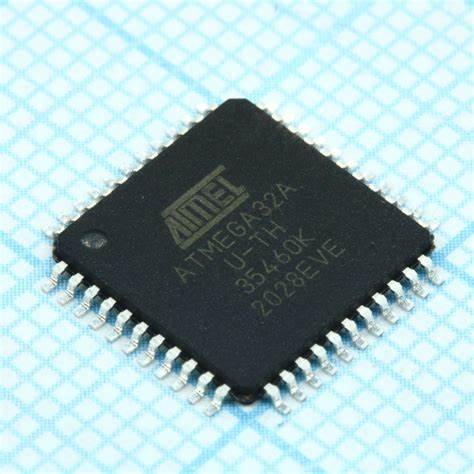
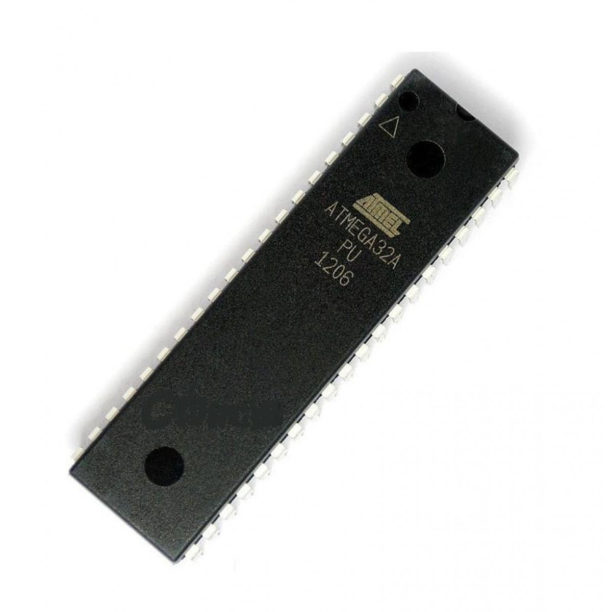
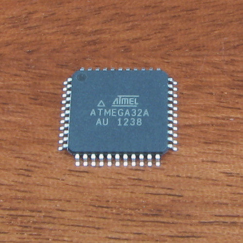
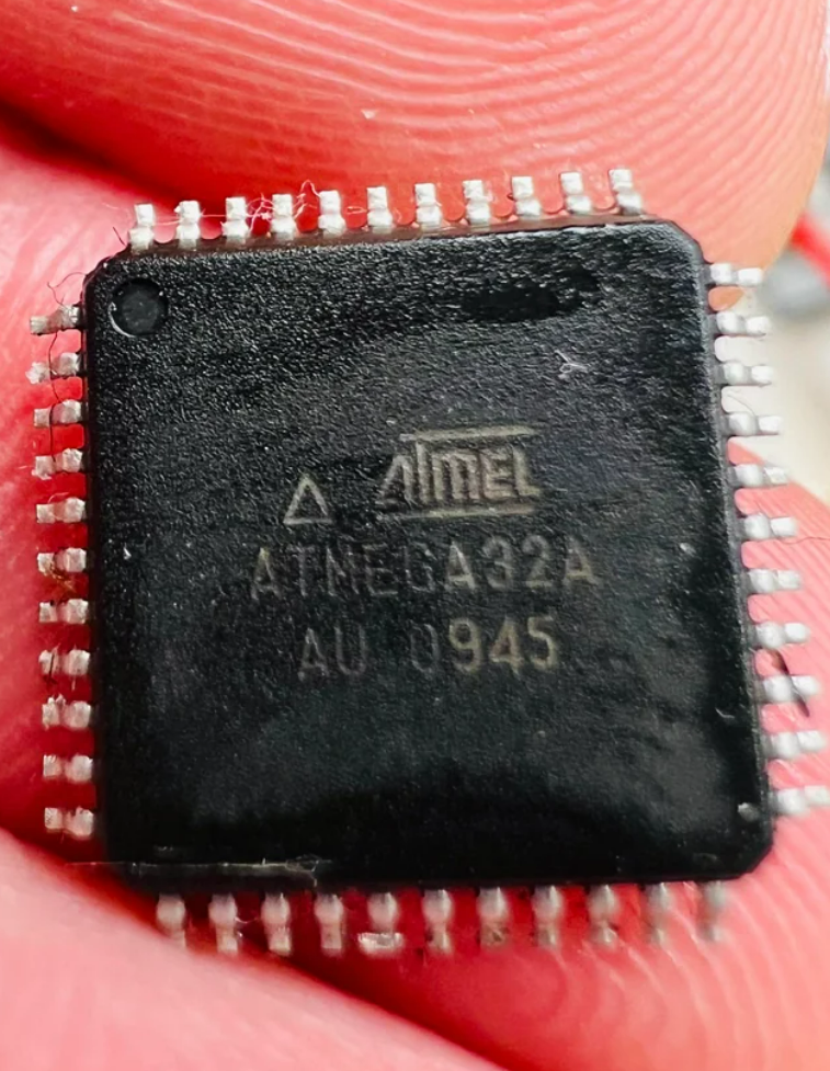
Break IC ATmega32A Software
Breaking IC ATmega32A software involves cracking or decoding the secured and encrypted firmware stored in the microcontroller’s flash memory and EEPROM memory. The ATmega32A MCU, like many modern microprocessors, is designed with protective measures to prevent unauthorized access to its program, binary, and source code. To unlock and restore this software, reverse engineering techniques are often employed.
breaking IC ATmega32A software involves cracking or decoding the secured and encrypted firmware stored in the ATmega32A microcontroller’s flash memory and EEPROM memory. The ATmega32A MCU, like many modern microprocessors, is designed with protective measures to prevent unauthorized access to its program, binary, and source code. To unlock and restore this software, reverse engineering techniques are often employed
The first step in breaking the IC’s software is to analyze the microprocessor’s architecture and security features. These security mechanisms, which may include encryption or lockouts, are intended to protect the integrity of the firmware. Once these protective layers are bypassed, the embedded program can be extracted from the flash memory and EEPROM memory. The extracted binary or heximal data is then decoded to retrieve the source code, which can be restored, cloned, or replicated for use in different applications.
Unlocking the ATmega32A software also opens the door to cloning the firmware for use in other devices or systems. This process ensures that the program can be duplicated for backup purposes or hardware replication. Additionally, breaking the software can allow for troubleshooting or upgrading the system, especially when original source code or design files are unavailable.
разбиване на IC Софтуерът ATmega32A включва кракване или декодиране на защитения и криптиран фърмуер, съхраняван във флаш паметта и EEPROM паметта на микроконтролера ATmega32A. ATmega32A MCU, подобно на много съвременни микропроцесори, е проектиран със защитни мерки за предотвратяване на неоторизиран достъп до неговата програма, двоичен и изходен код. За отключване и възстановяване на този софтуер често се използват техники за обратно инженерство
While breaking IC ATmega32A software can be a valuable technique for system recovery or hardware maintenance, it is essential to operate within legal and ethical boundaries. Unauthorized cracking, decoding, or cloning of software can violate intellectual property rights and lead to legal consequences. Proper authorization and adherence to intellectual property laws are essential when performing these activities.
We can Break IC ATMEGA32A Software, please view the IC ATMEGA32A features for your reference:
In order to maximize performance and parallelism, the AVR uses a Harvard architecture – with separate memories and buses for program and data. Instructions in the program memory are executed with a single level pipelining. While one instruction is being executed, the next instruction is pre-fetched from the program memory. This concept enables instructions to be executed in every clock cycle. The program memory is In-System Reprogrammable Flash memory. The fast-access Register File contains 32 x 8-bit general purpose working registers with a single clock cycle access time. This allows single-cycle Arithmetic Logic Unit (ALU) operation. In a typical ALU operation, two operands are output from the Register File, the operation is executed, and the result is stored back in the Register File – in one clock cycle. Six of the 32 registers can be used as three 16-bit indirect address register pointers for Data Space addressing – enabling efficient address calculations before Break IC.
One of the these address pointers can also be used as an address pointer for look up tables in Flash Program memory. These added function registers are the 16-bit X-, Y-, and Z-register, described later in this section. The ALU supports arithmetic and logic operations between registers or between a constant and a register. Single register operations can also be executed in the ALU. After an arithmetic operation, the Status Register is updated to reflect information about the result of the operation. Program flow is provided by conditional and unconditional jump and call instructions, able to directly address the whole address space. Most AVR instructions have a single 16-bit word format when Break IC.
IC ATmega32A yazılımını kırmak, ATmega32A mikrodenetleyicisinin flaş belleğinde ve EEPROM belleğinde saklanan güvenli ve şifreli aygıt yazılımını kırmayı veya kodunu çözmeyi içerir. ATmega32A MCU, birçok modern mikroişlemci gibi, programına, ikili dosyasına ve kaynak koduna yetkisiz erişimi önlemek için koruyucu önlemlerle tasarlanmıştır. Bu yazılımın kilidini açmak ve geri yüklemek için genellikle tersine mühendislik teknikleri kullanılır
Every program memory address contains a 16- or 32-bit instruction. Program Flash memory space is divided in two sections, the Boot program section and the Application Program section. Both sections have dedicated Lock bits for write and break/write protection. The SPM instruction that writes into the Application Flash memory section must reside in the Boot Program section. During interrupts and subroutine calls, the return address Program Counter (PC) is stored on the Stack. The Stack is effectively allocated in the general data SRAM, and consequently the Stack size is only limited by the total SRAM size and the usage of the SRAM. All user programs must initialize the SP in the reset routine (before subroutines or interrupts are executed). The Stack Pointer SP is break/write accessible in the I/O space.
The data SRAM can easily be accessed through the five different addressing modes supported in the AVR architecture. The memory spaces in the AVR architecture are all linear and regular memory maps. A flexible interrupt module has its control registers in the I/O space with an additional global interrupt enable bit in the Status Register. All interrupts have a separate interrupt vector in the interrupt vector table after Break IC.
IC ATmega32A 소프트웨어를 깨는 것은 ATmega32A 마이크로컨트롤러의 플래시 메모리와 EEPROM 메모리에 저장된 보안되고 암호화된 펌웨어를 크래킹하거나 디코딩하는 것을 포함합니다. 많은 최신 마이크로프로세서와 마찬가지로 ATmega32A MCU는 프로그램, 바이너리 및 소스 코드에 대한 무단 액세스를 방지하기 위한 보호 조치로 설계되었습니다. 이 소프트웨어의 잠금을 해제하고 복원하기 위해 종종 역엔지니어링 기술이 사용됩니다.
The interrupts have priority in accordance with their interrupt vector position. The lower the interrupt vector address, the higher the priority. The I/O memory space contains 64 addresses for CPU peripheral functions as Control Registers, SPI, and other I/O functions. The I/O Memory can be accessed directly, or as the Data Space locations following those of the Register File, $20 – $5F.
Recover Microcontroller ATmega32PA Firmware
We can Recover Microcontroller ATmega32PA Firmware, please view the Microcontroller ATmega32PA features for your reference:
Port A serves as the analog inputs to the A/D Converter.
Port A also serves as an 8-bit bi-directional I/O port, if the A/D Converter is not used. Port pins can provide internal pull-up resistors (selected for each bit). The Port A output buffers have symmetrical drive characteristics with both high sink and source capability.
When pins PA0 to PA7 are used as inputs and are externally pulled low, they will source current if the internal pull-up resistors are activated. The Port A pins are tri-stated when a reset condition becomes active, even if the clock is not running before Extract PLD IC Source Code.
Port B is an 8-bit bi-directional I/O port with internal pull-up resistors (selected for each bit). The Port B output buffers have symmetrical drive characteristics with both high sink and source capability. As inputs, Port B pins that are externally pulled low will source current if the pull-up resistors are activated.
The Port B pins are tri-stated when a reset condition becomes active, even if the clock is not running. Port C is an 8-bit bi-directional I/O port with internal pull-up resistors (selected for each bit). The Port C output buffers have symmetrical drive characteristics with both high sink and source capability. As inputs, Port C pins that are externally pulled low will source current if the pull-up resistors are activated before Break IC ATmega32A Software.
The Port C pins are tri-stated when a reset condition becomes active, even if the clock is not running. If the JTAG interface is enabled, the pull-up resistors on pins PC5(TDI), PC3(TMS) and PC2(TCK) will be activated even if a reset occurs. The TD0 pin is tri-stated unless TAP states that shift out data are entered.
Port D is an 8-bit bi-directional I/O port with internal pull-up resistors (selected for each bit). The Port D output buffers have symmetrical drive characteristics with both high sink and source capability. As inputs, Port D pins that are externally pulled low will source current if the pull-up resistors are activated.
The Port D pins are tri-stated when a reset condition becomes active, even if the clock is not running. Reset Input. A low level on this pin for longer than the minimum pulse length will generate a reset, even if the clock is not running. The minimum pulse length is given in Table 15 on page 37.
Shorter pulses are not guaranteed to generate a reset. Input to the inverting Oscillator amplifier and input to the internal clock operating circuit Output from the inverting Oscillator amplifier. AVCC is the supply voltage pin for Port A and the A/D Converter. It should be externally connected to VCC, even if the ADC is not used. If the ADC is used, it should be connected to VCC through a low-pass filter.
AREF is the analog reference pin for the A/D Converter. A comprehensive set of development tools, application notes and datasheets are available for download on http://www.atmel.com/avr. This documentation contains simple code examples that briefly show how to use various parts of the device. These code examples assume that the part specific header file is included before compilation after MCU Cracking Process. Be aware that not all C Compiler vendors include bit definitions in the header files and interrupt handling in C is compiler dependent.
Break MCU ATMEGA16PA Flash
Break MCU ATMEGA16PA Flash
We can Break MCU ATmega16PA Flash, please view the Mcu ATMEGA16PA features for your reference:
First Analog Comparator conversion may be delayed. If the device is powered by a slow rising VCC, the first Analog Comparator conversion will take longer than expected on some devices by Crack MCU.
Problem Fix/Workaround
When the device has been powered or reset, disable then enable theAnalog Comparator before the first conversion.
Interrupts may be lost when writing the timer registers in the asynchronous timer
The interrupt will be lost if a timer register that is synchronized to the asynchronous timer clock is written when the asynchronous Timer/Counter register(TCNTx) is 0x00 if Break MCU ATMEGA16PA Flash.
Problem Fix / Workaround
Always check that the asynchronous Timer/Counter register neither have the value 0xFF nor 0x00 before writing to the asynchronous Timer Control Register(TCCRx), asynchronous Timer Counter Register(TCNTx), or asynchronous Output Compare Register(OCRx).
IDCODE masks data from TDI input, The JTAG instruction IDCODE is not working correctly. Data to succeeding devices are replaced by all-ones during Update-DR in the process of Recover Chip PIC16F620A Binary.
Problem Fix / Workaround
If ATmega16 is the only device in the scan chain, the problem is not visible. Select the Device ID Register of the ATmega16 by issuing the IDCODE instruction or by entering the Test-Logic-Reset state of the TAP controller to break out the contents of its Device ID Register and possibly data from succeeding devices of the scan chain.
Issue the BYPASS instruction to the ATmega16 while breaking the Device ID Registers of preceding devices of the boundary scan chain. If the Device IDs of all devices in the boundary scan chain must be captured simultaneously, the ATmega16 must be the fist device in the chain to facilitate the progress of Recover Chip PIC16C621 Program.
Breaking EEPROM by using ST or STS to set EERE bit triggers unexpected interrupt request.
Breaking EEPROM by using the ST or STS command to set the EERE bit in the EECR register triggers an unexpected EEPROM interrupt request.
Problem Fix / Workaround
Always use OUT or SBI to set EERE in EECR.
First Analog Comparator conversion may be delayed
If the device is powered by a slow rising VCC, the first Analog Comparator conversion will take longer than expected on some devices.
Problem Fix/Workaround
When the device has been powered or reset, disable then enable theAnalog Comparator before the first conversion. Interrupts may be lost when writing the timer registers in the asynchronous timer, The interrupt will be lost if a timer register that is synchronized to the asynchronous timer clock is written when the asynchronous Timer/Counter register(TCNTx) is 0x00.
Problem Fix / Workaround
Always check that the asynchronous Timer/Counter register neither have the value 0xFF nor 0x00 before writing to the asynchronous Timer Control Register(TCCRx), asynchronous Timer Counter Register(TCNTx), or asynchronous Output Compare Register(OCRx).
IDCODE masks data from TDI input
The JTAG instruction IDCODE is not working correctly. Data to succeeding devices are replaced by all-ones during Update-DR.
Problem Fix / Workaround
If ATmega16 is the only device in the scan chain, the problem is not visible.
Select the Device ID Register of the ATmega16 by issuing the IDCODE instruction or by entering the Test-Logic-Reset state of the TAP controller to break out the contents of its Device ID Register and possibly data from succeeding devices of the scan chain. Issue the BYPASS instruction to the ATmega16 while breaking the Device ID.
Registers of preceding devices of the boundary scan chain. If the Device IDs of all devices in the boundary scan chain must be captured simultaneously by Reverse Engineering Microcontroller PIC16C620 Code, the ATmega16 must be the fist device in the chain.
Breaking EEPROM by using ST or STS to set EERE bit triggers unexpected interrupt request.
Breaking EEPROM by using the ST or STS command to set the EERE bit in the EECR register triggers an unexpected EEPROM interrupt request.
Problem Fix / Workaround
Always use OUT or SBI to set EERE in EECR.
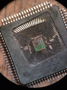
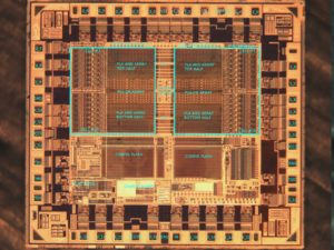
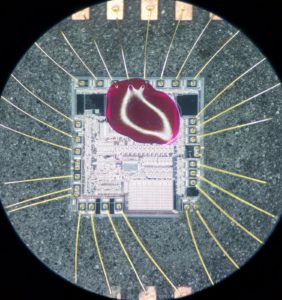
Recover Microcontroller ATmega16A Software
Recovering microcontroller ATmega16A software involves cracking or decoding the secured firmware stored in the secured MCU’s flash memory and EEPROM memory. The ATmega16A, like many MCUs, is designed with protective features to lock its binary and heximal data, making it challenging to access the embedded software without proper tools and techniques. To unlock the firmware, reverse engineering methods are often employed to bypass encryption protocols and retrieve the source code.
Il recupero del software del microcontrollore ATmega16A comporta il cracking o la decodifica del firmware protetto archiviato nella memoria flash e nella memoria EEPROM dell’MCU protetta. L’ATmega16A, come molti MCU, è progettato con funzionalità di protezione per bloccare i suoi dati binari ed esadecimali, rendendo difficile l’accesso al software incorporato senza strumenti e tecniche adeguati. Per sbloccare il firmware, vengono spesso impiegati metodi di reverse engineering per bypassare i protocolli di crittografia e recuperare il codice sorgente.
Once the locked software is unlocked, it can be restored to its original functionality, or cloned for use in other systems. This process is crucial when the program has been corrupted, lost, or when hardware replication is necessary. By extracting and recovering the program, engineers can ensure that systems relying on the ATmega16A MCU can continue operating without the need for expensive replacements.
However, recovering software from a microcontroller must be done ethically, ensuring compliance with legal standards regarding intellectual property rights.
Recover Microcontroller ATmega16A Software
We can Recover Microcontroller ATmega16A Software, please view the Microcontroller ATmega16A features for your reference:
First Analog Comparator conversion may be delayed
If the device is powered by a slow rising VCC, the first Analog Comparator conversion will take longer than expected on some devices.
Problem Fix/Workaround
When the device has been powered or reset, disable then enable theAnalog Comparator before the first conversion. Interrupts may be lost when writing the timer registers in the asynchronous time to Break IC PIC16C74 Code. The interrupt will be lost if a timer register that is synchronized to the asynchronous timer clock is written when the asynchronous Timer/Counter register(TCNTx) is 0x00 if Recover Microcontroller ATmega16A Software.
माइक्रोकंट्रोलर ATmega16A सॉफ़्टवेयर को पुनर्प्राप्त करने में सुरक्षित MCU की फ़्लैश मेमोरी और EEPROM मेमोरी में संग्रहीत सुरक्षित फ़र्मवेयर को क्रैक या डिकोड करना शामिल है। कई MCU की तरह, ATmega16A को इसके बाइनरी और हेक्सिमल डेटा को लॉक करने के लिए सुरक्षात्मक सुविधाओं के साथ डिज़ाइन किया गया है, जिससे उचित उपकरणों और तकनीकों के बिना एम्बेडेड सॉफ़्टवेयर तक पहुँचना चुनौतीपूर्ण हो जाता है। फ़र्मवेयर को अनलॉक करने के लिए, एन्क्रिप्शन प्रोटोकॉल को बायपास करने और स्रोत कोड को पुनः प्राप्त करने के लिए अक्सर रिवर्स इंजीनियरिंग विधियों का उपयोग किया जाता है।
Problem Fix / Workaround
Always check that the asynchronous Timer/Counter register neither have the value 0xFF nor 0x00 before writing to the asynchronous Timer Control Register(TCCRx), asynchronous Timer Counter Register(TCNTx), or asynchronous Output Compare Register(OCRx) for the purpose of Copy Chip PIC16C73A Program.
IDCODE masks data from TDI input
The JTAG instruction IDCODE is not working correctly. Data to succeeding devices are replaced by all-ones during Update-DR.
Problem Fix / Workaround
If ATmega16 is the only device in the scan chain, the problem is not visible.
Select the Device ID Register of the ATmega16 by issuing the IDCODE instruction or by entering the Test-Logic-Reset state of the TAP controller to recover out the contents of its Device ID Register and possibly data from succeeding devices of the scan chain. Issue the BYPASS instruction to the ATmega16 while recovering the Device ID Registers of preceding devices of the boundary scan chain before Recover Microcontroller ATmega16A Software.
If the Device IDs of all devices in the boundary scan chain must be captured simultaneously, the ATmega16 must be the fist device in the chain of Reverse Engineering Microcontroller PIC16F73 Program.
Recovering EEPROM by using ST or STS to set EERE bit triggers unexpected interrupt request.
Recovering EEPROM by using the ST or STS command to set the EERE bit in the EECR register triggers an unexpected EEPROM interrupt request.
Problem Fix / Workaround
Always use OUT or SBI to set EERE in EECR.
First Analog Comparator conversion may be delayed to Unlock Microcontroller, Interrupts may be lost when writing the timer registers in the asynchronous timer IDCODE masks data from TDI input
نرم افزار بازیابی میکروکنترلر ATmega16A شامل شکستن یا رمزگشایی سیستم عامل ایمن ذخیره شده در حافظه فلش MCU ایمن و حافظه EEPROM است. ATmega16A، مانند بسیاری از MCU ها، با ویژگی های محافظتی طراحی شده است تا داده های باینری و هگزیمال خود را قفل کند، و دسترسی به نرم افزار تعبیه شده بدون ابزار و تکنیک های مناسب را دشوار می کند. برای باز کردن قفل سفتافزار، اغلب از روشهای مهندسی معکوس برای دور زدن پروتکلهای رمزگذاری و بازیابی کد منبع استفاده میشود.
Recovering EEPROM by using ST or STS to set EERE bit triggers unexpected interrupt request. First Analog Comparator conversion may be delayed before Recover Microcontroller ATmega16A Software
If the device is powered by a slow rising VCC, the first Analog Comparator conversion will take longer than expected on some devices after Recover MCU PIC16C72 Software.
Problem Fix/Workaround
When the device has been powered or reset, disable then enable theAnalog Comparator before the first conversion.
Recover MCU TS87C58X2 Heximal
Recover MCU TS87C58X2 Heximal
We can Recover Mcu TS87C58X2 Heximal, please view the Mcu TS87C58X2 features for your reference:
The automatic address recognition feature is enabled when the multiprocessor communication feature is enabled (SM2 bit in SCON register is set). Implemented in hardware, automatic address recognition enhances the multiprocessor communication feature by allowing the serial port to examine the address of each incoming command frame.
Only when the serial port recognizes its own address, the receiver sets RI bit in SCON register to generate an interrupt. This ensures that the CPU is not interrupted by command frames addressed to other devices if Recover MCU TS87C58X2 Heximal.
If desired, you may enable the automatic address recognition feature in mode 1. In this configuration, the stop bit takes the place of the ninth data bit. Bit RI is set only when the received command frame address matches the device’s address and is terminated by a valid stop bit.
To support automatic address recognition, a device is identified by a given address and a broadcast address. Each device has an individual address that is specified in SADDR register; the SADEN register is a mask byte that contains don’t-care bits (defined by zeros) to form the device’s given address.
The don’t-care bits provide the flexibility to address one or more slaves at a time. The following example illustrates how a given address is formed. To address a device by its individual address, the SADEN mask byte must be 1111 1111b if Recover MCU TS87C58X2 Heximal.
The SADEN byte is selected so that each slave may be addressed separately. For slave A, bit 0 (the LSB) is a don’t-care bit; for slaves B and C, bit 0 is a 1. To communicate with slave A only, the master must send an address where bit 0 is clear (e.g. 1111 0000b).
For slave A, bit 1 is a 1; for slaves B and C, bit 1 is a don’t care bit. To communicate with slaves B and C, but not slave A, the master must send an address with bits 0 and 1 both set (e.g. 1111 0011b). To communicate with slaves A, B and C, the master must send an address with bit 0 set, bit 1 clear, and bit 2 clear (e.g. 1111 0001b).
On reset, the SADDR and SADEN registers are initialized to 00h, i.e. the given and broadcast addresses are XXXX XXXXb (all don’t-care bits). This ensures that the serial port will reply to any address, and so, that it is backwards compatible with the 80C51 mcus that do not support automatic address recognition after Recover MCU.
Break IC TS80C58X2 Code
We can Break IC TS80C58X2 Code, please view the IC TS80C58X2 features for your reference:
Software can take advantage of the additional data pointers to both increase speed and reduce code size, for example, block operations (copy, compare, search …) are well served by using one data pointer as a ’source’ pointer and the other one as a “destination” pointer.
INC is a short (2 bytes) and fast (12 clocks) way to manipulate the DPS bit in the AUXR1 SFR. However, note that the INC instruction does not directly force the DPS bit to a particular state, but simply toggles it.
In simple routines, such as the block move example, only the fact that DPS is toggled in the proper sequence matters, not its actual value. In other words, the block move routine works the same whether DPS is ‘0’ or ‘1’ on entry. Observe that without the last instruction (INC AUXR1), the routine will exit with DPS in the opposite state.
The timer 2 in the TS80C54/58X2 is compatible with the timer 2 in the 80C52. It is a 16-bit timer/counter: the count is maintained by two eight-bit timer registers, TH2 and TL2, connected in cascade. It is controlled by T2CON register (See Table 6) and T2MOD register (See Table 7) after Break IC TS80C58X2 Code.
Timer 2 operation is similar to Timer 0 and Timer 1. C/T2 selects FOSC/12 (timer operation) or external pin T2 (counter operation) as the timer clock input. Setting TR2 allows TL2 to be incremented by the selected input.
Timer 2 has 3 operating modes: capture, autoreload and Baud Rate Generator. These modes are selected by the combination of RCLK, TCLK and CP/RL2 (T2CON), as described in the Atmel Wireless & Microcontrollers 8-bit Microcontroller Hardware description.
Refer to the Atmel Wireless & Microcontrollers 8-bit Microcontroller Hardware description for the description of Capture and Baud Rate Generator Modes. In TS80C54/58X2 Timer 2 includes the following enhancements:
Auto-reload mode with up or down counter
Programmable clock-output
The auto-reload mode configures timer 2 as a 16-bit timer or event counter with automatic reload. If DCEN bit in T2MOD is cleared, timer 2 behaves as in 80C52 (refer to the Atmel Wireless & Microcontrollers 8-bit Microcontroller Hardware description). If DCEN bit is set, timer 2 acts as an Up/down timer/counter as shown in Figure 4. In this mode the T2EX pin controls the direction of count.
Break IC TS80C58X2 Code
When T2EX is high, timer 2 counts up. Timer overflow occurs at FFFFh which sets the TF2 flag and generates an interrupt request. The overflow also causes the 16-bit value in RCAP2H and RCAP2L registers to be loaded into the timer registers TH2 and TL2.
When T2EX is low, timer 2 counts down. Timer underflow occurs when the count in the timer registers TH2 and TL2 equals the value stored in RCAP2H and RCAP2L registers. The underflow sets TF2 flag and reloads FFFFh into the timer registers.
The EXF2 bit toggles when timer 2 overflows or underflows according to the the direction of the count. EXF2 does not generate any interrupt. This bit can be used to provide 17-bit resolution.
Recover Mcu TS80C54X2 Flash
We can Recover Mcu TS80C54X2 Flash, please view the Mcu TS80C54X2 features for your reference:
TS80C54/58X2 is high performance CMOS ROM, OTP and EPROM versions of the 80C51 CMOS single chip 8-bit mcu. The TS80C54/58X2 retains all features of the Atmel Wireless & Mcus 80C51 with extended ROM/EPROM capacity (16/32 Kbytes), 256 bytes of internal RAM, a 6-source , 4-level interrupt system, an on-chip oscilator and three timer/counters.
In addition, the TS80C54/58X2 has a Hardware Watchdog Timer, a more versatile serial channel that facilitates multiprocessor communication (EUART) and a X2 speed improvement mechanism.
The fully static design of the TS80C54/58X2 allows to reduce system power consumption by bringing the clock frequency down to any value, even DC, without loss of data before Recover Mcu TS80C54X2 Flash.
The TS80C54/58X2 has 2 software-selectable modes of reduced activity for further reduction in power consumption. In the idle mode the CPU is frozen while the timers, the serial port and the interrupt system are still operating. In the power-down mode the RAM is saved and all other functions are inoperative after Recover Mcu.
80C52 Compatible
8051 pin and instruction compatible
Four 8-bit I/O ports
Three 16-bit timer/counters
256 bytes scratchpad RAM
High-Speed Architecture
40 MHz @ 5V, 30MHz @ 3V
Recover Mcu TS80C54X2 Flash
X2 Speed Improvement capability (6 clocks/machine cycle)
30 MHz @ 5V, 20 MHz @ 3V (Equivalent to 60 MHz @ 5V, 40 MHz @ 3V)
Dual Data Pointer if Recover Mcu
On-chip ROM/EPROM (16K-bytes, 32K-bytes)
Programmable Clock Out and Up/Down Timer/
Counter 2
Hardware Watchdog Timer (One-time enabled with Reset-Out)
Asynchronous port reset
Interrupt Structure with
6 Interrupt sources
4 level priority interrupt system
Full duplex Enhanced UART before Recover Mcu
Framing error detection
Low EMI (inhibit ALE)
Power Control modes
Idle mode
Power-down mode
Power-off Flag
Once mode (On-chip Emulation)
Power supply: 4.5-5.5V, 2.7-5.5V
Temperature ranges: Commercial (0 to 70oC) and Industrial (-40 to 85oC)
Packages: PDIL40, PLCC44, VQFP44 1.4, PQFP44
F1, CQPJ44 (window), CDIL40 (window)
Recover MCU TS87C51U2 Heximal
Recover MCU TS87C51U2 Heximal
We can Recover MCU TS87C51U2 Heximal, please view the MCU TS87C51U2 features for your reference:
In comparison to the original 80C52, the TS80C51U2 implements some new features, which are:
The X2 option.
The second full duplex enhanced UART
The Baud Rate generator.
The Dual Data Pointer.
The Watchdog.
The 4 level interrupt priority system
The power-off flag.
The ONCE mode.
The ALE disabling.
Some enhanced features are also located in the UARTs and the timer 2.
The TS80C51U2 core needs only 6 clock periods per machine cycle. This feature called ”X2” provides the following advantages:
Divide frequency crystals by 2 (cheaper crystals) while keeping same CPU power. Save power consumption while keeping same CPU power (oscillator power saving). Save power consumption by dividing dynamically operating frequency by 2 in operating and idle modes after Recover MCU.
Increase CPU power by 2 while keeping same crystal frequency. In order to keep the original C51 compatibility, a divider by 2 is inserted between the XTAL1 signal and the main clock input of the core (phase generator). This divider may be disabled by software if Recover MCU TS87C51U2 Heximal.
Recover MCU TS87C51U2 Heximal
The clock for the whole circuit and peripheral is first divided by two before being used by the CPU core and peripherals. This allows any cyclic ratio to be accepted on XTAL1 input. In X2 mode, as this divider is bypassed, the signals on XTAL1 must have a cyclic ratio between 40 to 60%. Figure 1.
shows the clock generation block diagram. X2 bit is validated on XTAL1÷2 rising edge to avoid glitches when switching from X2 to STD mode. Figure 2. shows the mode switching waveforms.
The X2 bit in the CKCON register (See Table 4.) allows to switch from 12 clock cycles per instruction to 6 clock cycles and vice versa. At reset, the standard speed is activated (STD mode). Setting this bit activates the X2 feature (X2 mode).
CAUTION
In order to prevent any incorrect operation while operating in X2 mode, user must be aware that all peripherals using clock frequency as time reference (UARTs, timers) will have their time reference divided by two. For example a free running timer generating an interrupt every 20 ms will then generate an interrupt every 10 ms. UART with 4800 baud rate will have 9600 baud rate if Recover MCU TS87C51U2 Heximal.
The additional data pointer can be used to speed up code execution and reduce code size in a number of ways. The dual DPTR structure is a way by which the chip will specify the address of an external data memory location. There are two 16-bit DPTR registers that address the external memory, and a single bit called DPS = AUXR1/bit0 (See Table 5.) that allows the program code to switch between them if Recover MCU.