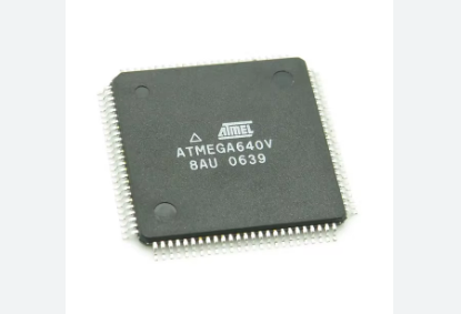
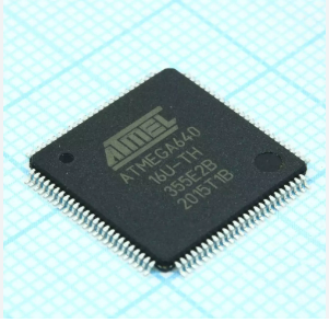
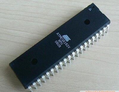
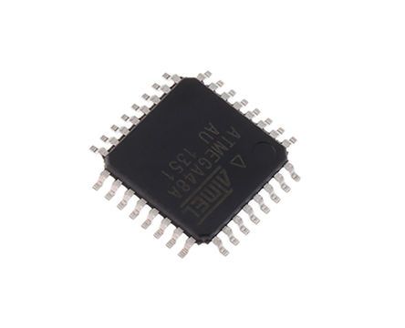
 Recover Microprocessor ATMEGA640V Firmware
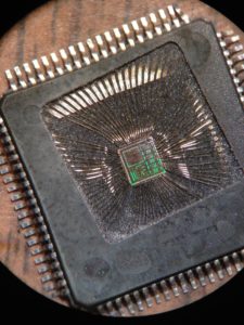
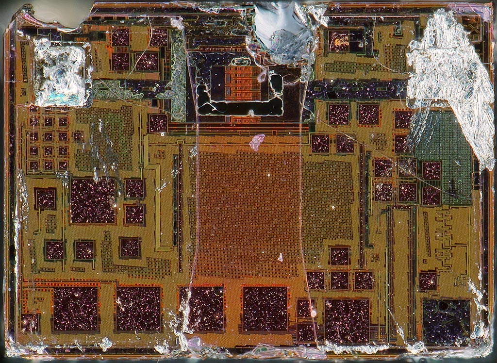
Recovering Microprocessor ATMEGA640V firmware is a highly technical process that often involves reverse engineering techniques to crack and decrypt the protected code stored within the microcontroller. The firmware, which operates at the core of the microprocessor’s functionality, is typically encoded in binary or hexadecimal (hex) format. To recover the ATMEGA640V firmware, engineers may need to decode this complex data and understand its structure, enabling them to copy and restore the original functions of the device.
Възстановяване на фърмуера на микропроцесор ATMEGA640V е изключително технически процес, който често включва техники за обратно инженерство за кракване и дешифриране на защитения код, съхраняван в микроконтролера. Фърмуерът, който работи в основата на функционалността на микропроцесора ATMEGA640V, обикновено е кодиран в двоичен или шестнадесетичен (шестнадесетичен) формат. За да възстановят фърмуера на ATMEGA640V, инженерите може да се наложи да декодират тези сложни данни и да разберат структурата им, което им позволява да копират и възстановят оригиналните функции на устройството.
In many cases, firmware recovery requires cracking the security features of the microcontroller (MCU), which are designed to prevent unauthorized access. This can involve analyzing the microprocessor’s internal architecture, exploiting vulnerabilities, or using specialized equipment to bypass encryption. Once decrypted, the binary or hex representation of the firmware can be decoded and reassembled for restoration or analysis.
Recover Microprocessor ATMEGA640V Firmware
We can recover microprocessor ATMEGA640V firmware, please view the microprocessor ATMEGA640V features for your reference:
XTAL1 and XTAL2 are the input and output, respectively, of an inverting amplifier that can be configured for use as an on-chip oscillator by Copy Microcontroller PIC12F675 Firmware. Either a quartz crystal or ceramic resonator may be used.
To drive the device from an external clock source, XTAL2 should be left unconnected while XTAL1 is driven, as shown in Figure 12.
There are no requirements on the duty cycle of the external clock signal, since the input to the internal clocking circuitry is through a divide-by-two flip-flop, but minimum and maximum voltage high and low time specifications must be observed if Recover Microprocessor ATmega640V Firmware.
माइक्रोप्रोसेसर ATMEGA640V फर्मवेयर को पुनर्प्राप्त करना एक अत्यधिक तकनीकी प्रक्रिया है जिसमें अक्सर माइक्रोकंट्रोलर के भीतर संग्रहीत संरक्षित कोड को क्रैक और डिक्रिप्ट करने के लिए रिवर्स इंजीनियरिंग तकनीक शामिल होती है। ATMEGA640V माइक्रोप्रोसेसर की कार्यक्षमता के मूल में संचालित होने वाला फर्मवेयर आमतौर पर बाइनरी या हेक्साडेसिमल (हेक्स) प्रारूप में एन्कोड किया जाता है। ATMEGA640V फर्मवेयर को पुनर्प्राप्त करने के लिए, इंजीनियरों को इस जटिल डेटा को डिकोड करने और इसकी संरचना को समझने की आवश्यकता हो सकती है, जिससे वे डिवाइस के मूल कार्यों को कॉपी और पुनर्स्थापित कर सकें।
In idle mode, the CPU puts itself to sleep while all the on-chip peripherals remain active in the process of Copy MCU PIC18F4685 Software. The mode is invoked by software. The content of the on-chip RAM and all the special functions registers remain unchanged during this mode. The idle mode can be terminated by any enabled interrupt or by a hardware reset.
Note that when idle mode is terminated by a hardware reset, the device normally resumes firmware execution from where it left off, up to two machine cycles before the internal reset algorithm takes control. On-chip hardware inhibits access to internal RAM in this event by Unlock Microcontroller Firmware, but access to the port pins is not inhibited.
To eliminate the possibility of an unexpected write to a port pin when idle mode is terminated by a reset for support the progress of Copy IC PIC18F458 Binary, the instruction following the one that invokes idle mode should not write to a port pin or to external memory.
بازیابی سیستم عامل میکروپروسسور ATMEGA640V یک فرآیند بسیار فنی است که اغلب شامل تکنیک های مهندسی معکوس برای شکستن و رمزگشایی کد محافظت شده ذخیره شده در میکروکنترلر است. سفتافزار، که در هسته عملکرد ریزپردازنده ATMEGA640V کار میکند، معمولاً در قالب باینری یا هگزا دسیمال (هگز) کدگذاری میشود. برای بازیابی سفتافزار ATMEGA640V، مهندسان ممکن است نیاز به رمزگشایی این دادههای پیچیده و درک ساختار آن داشته باشند و آنها را قادر میسازد تا عملکردهای اصلی دستگاه را کپی و بازیابی کنند.
In the power down mode, the oscillator is stopped and the instruction that invokes power down is the last instruction executed. The on-chip RAM and Special Function Registers retain their values until the power down mode is terminated.
Exit from power down can be initiated either by a hardware reset or by an enabled external interrupt. Reset redefines the SFRs but does not change the on-chip RAM. The reset should not be activated before VCC is restored to its normal operating level and must be held active long enough to allow the oscillator to restart and stabilize before Recover Chip MC9S08DZ32ACLC Firmware.
To exit power down via an interrupt, the external interrupt must be enabled as level sensitive before entering power down. The interrupt service routine starts at 16 ms (nominal) after the enabled interrupt pin is activated.
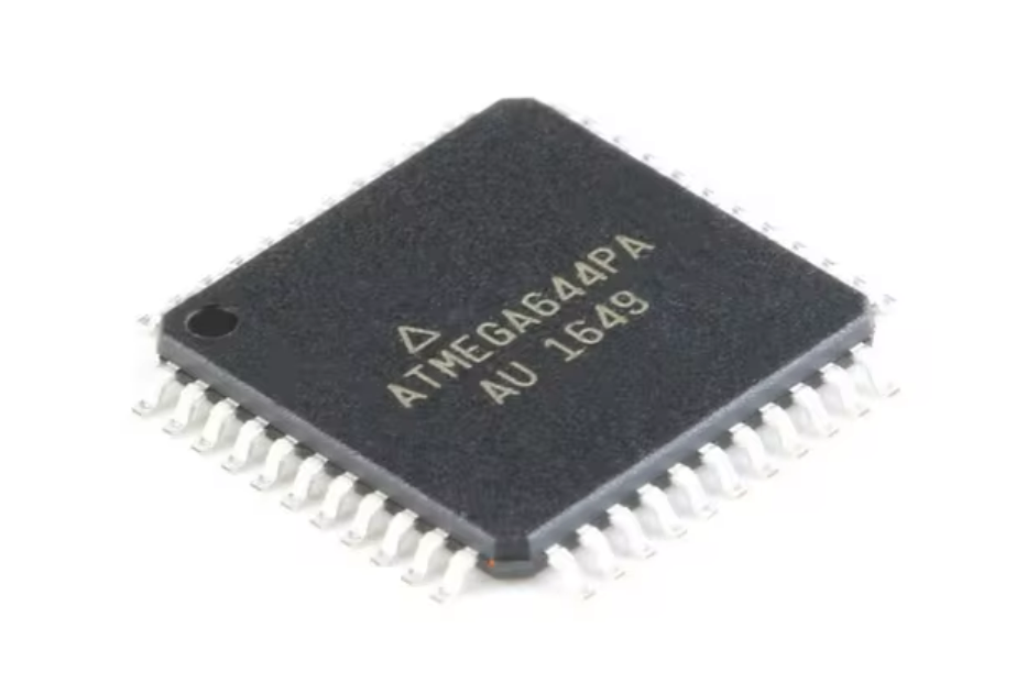
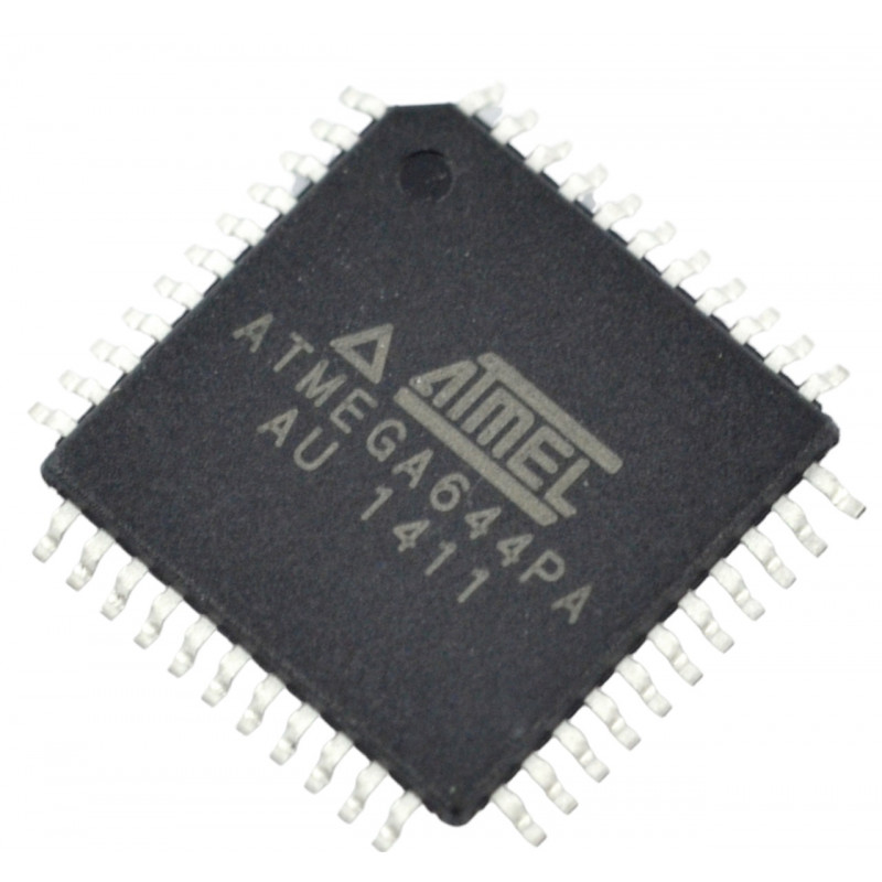
Reverse Engineering Microcontroller ATmega644PA Firmware
Reverse engineering Microcontroller ATmega644PA firmware involves decoding and analyzing the embedded firmware stored within its flash memory program. Engineers often seek to recover or clone this microcontroller’s source code for testing, replication, or troubleshooting purposes. The ATmega644PA, known for its robust design in embedded systems, stores critical program instructions as binary data in EEPROM and flash memory, ensuring reliable functionality.
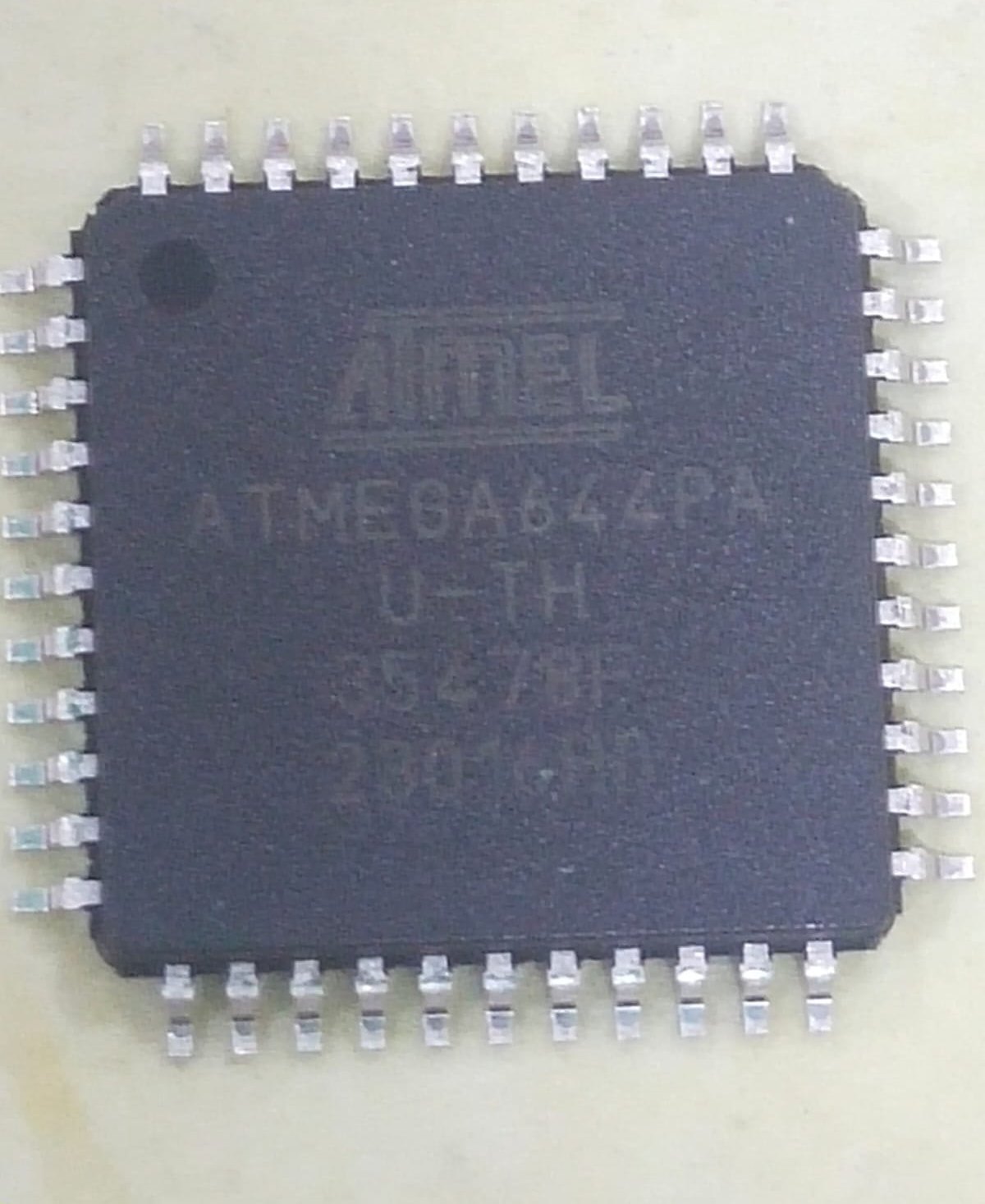
Beim Reverse Engineering der Firmware des Mikrocontrollers ATmega644PA geht es um das Dekodieren und Analysieren der eingebetteten Firmware, die in seinem Flash-Speicherprogramm gespeichert ist. Ingenieure versuchen häufig, den Quellcode dieses Mikrocontrollers zu Test-, Replikations- oder Fehlerbehebungszwecken wiederherzustellen oder zu klonen. Der ATmega644PA, der für sein robustes Design in eingebetteten Systemen bekannt ist, speichert kritische Programmbefehle als Binärdaten im EEPROM und Flash-Speicher und gewährleistet so eine zuverlässige Funktionalität.
To break through security features protecting this firmware, reverse engineering techniques must be employed to decode the program into a readable heximal file. This file format allows engineers to analyze the binary data and reconstruct the original source code, providing insights into how the microcontroller operates under different conditions. Recovering and cloning the ATmega644PA’s firmware requires precision to avoid data corruption, particularly as accessing EEPROM memory data often triggers security locks.
By managing each stage of the reverse engineering process carefully, engineers can maintain the integrity of the microcontroller’s program, ensuring any recovered source code is accurate and reliable. This process can be essential for device maintenance, compatibility testing, or creating compatible hardware designs that rely on the ATmega644PA’s core functions.
Reverse Engineering Microcontroller ATmega644PA Firmware
Note that if a level triggered interrupt is used for wake-up from Power-down mode, the changed level must be held for some time to wake up the procedures of Reverse Engineering Microcontroller ATmega644PA Firmware.
Refer to “External Interrupts”. When waking up from Power-down mode, there is a delay from the wake-up condition occurs until the wake-up becomes effective by Recover IC ST62T65C6 Software. This allows the clock to restart and become stable after having been stopped.
रिवर्स इंजीनियरिंग माइक्रोकंट्रोलर ATmega644PA फर्मवेयर में इसके फ्लैश मेमोरी प्रोग्राम में संग्रहीत एम्बेडेड फर्मवेयर को डिकोड करना और उसका विश्लेषण करना शामिल है। इंजीनियर अक्सर परीक्षण, प्रतिकृति या समस्या निवारण उद्देश्यों के लिए इस माइक्रोकंट्रोलर के स्रोत कोड को पुनर्प्राप्त या क्लोन करना चाहते हैं। एम्बेडेड सिस्टम में अपने मजबूत डिजाइन के लिए जाना जाने वाला ATmega644PA, महत्वपूर्ण प्रोग्राम निर्देशों को EEPROM और फ्लैश मेमोरी में बाइनरी डेटा के रूप में संग्रहीत करता है, जिससे विश्वसनीय कार्यक्षमता सुनिश्चित होती है।
The wake-up period is defined by the same CKSEL Fuses that define the Reset Time-out period, as described in “Clock Sources” on page 40. When the SM2..0 bits are written to 011, the SLEEP instruction makes the MCU Cracking enter Power-save mode.
This mode is identical to Power-down, with one exception: If Timer/Counter2 is enabled, it will keep running during sleep. The device can wake up from either Timer Overflow or Output Compare event from Timer/Counter2 if the corresponding Timer/Counter2 interrupt enable bits are set in TIMSK2 to facilitate the process of Attack MCU MSP430G2452IPW14R Heximal, and the Global Interrupt Enable bit in SREG is set.
If Timer/Counter2 is not running, Power-down mode is recommended instead of Power-save mode. The Timer/Counter2 can be clocked both synchronously and asynchronously in Power-save mode. If the Timer/Counter2 is not using the asynchronous clock, the Timer/Counter Oscillator is stopped during sleep.
سیستم عامل میکروکنترلر ATmega644PA مهندسی معکوس شامل رمزگشایی و تجزیه و تحلیل سیستم عامل تعبیه شده ذخیره شده در برنامه حافظه فلش خود است. مهندسان اغلب به دنبال بازیابی یا شبیه سازی کد منبع این میکروکنترلر برای اهداف آزمایش، تکرار یا عیب یابی هستند. ATmega644PA که به دلیل طراحی قوی خود در سیستمهای تعبیهشده شناخته میشود، دستورالعملهای برنامه حیاتی را به عنوان دادههای باینری در EEPROM و حافظه فلش ذخیره میکند و از عملکرد قابل اعتماد اطمینان میدهد.
If the Timer/Counter2 is not using the synchronous clock, the clock source is stopped during sleep. Note that even if the synchronous clock is running in Power-save, this clock is only available for the Timer/Counter2 in order to Attack IC TMS320F28232PGFA Software.
When the SM2..0 bits are 110 and an external crystal/resonator clock option is selected, the SLEEP instruction makes the MCU enter Standby mode. This mode is identical to Power-down with the exception that the Oscillator is kept running. From Standby mode, the device wakes up in six clock cycles.
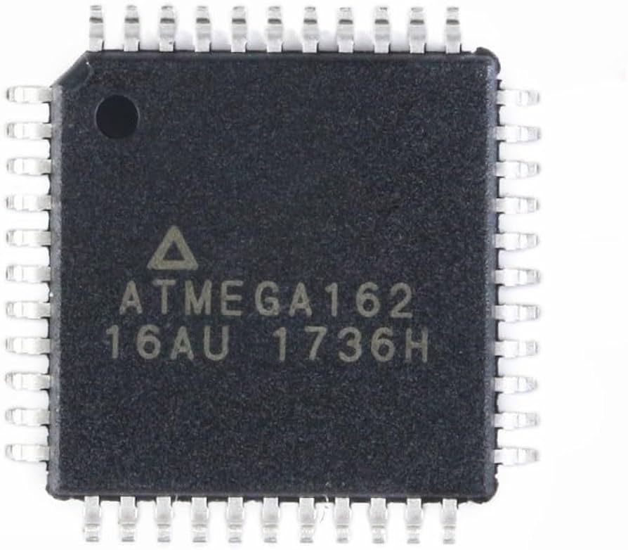
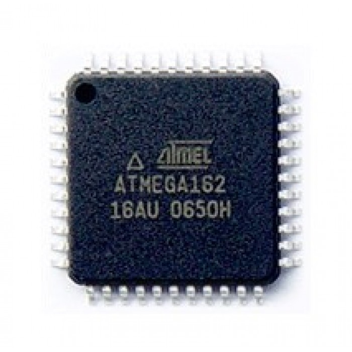
Recover MCU ATMEGA162A Heximal
Recovering MCU ATMEGA162A heximal data is a meticulous process involving advanced techniques to decode and restore the embedded firmware stored within this microcontroller’s flash memory program. This task may arise when source code or program data becomes corrupted, lost, or requires duplication for compatible systems. The ATMEGA162A MCU, known for its reliability in embedded applications, stores critical information in binary format within its EEPROM and flash memory.
recovering MCU ATMEGA162A heximal data is a meticulous process involving advanced techniques to decode and restore the embedded firmware stored within this microcontroller’s flash memory program. This task may arise when source code or program data becomes corrupted, lost, or requires duplication for compatible systems. The ATMEGA162A MCU, known for its reliability in embedded applications, stores critical information in binary format within its EEPROM and flash memory
To recover the heximal file, reverse engineering tools are often used to break the security layers protecting the firmware. This process involves decoding the binary data and converting it into a heximal file that represents the original source code. By reconstructing the code, engineers can clone or duplicate the program for testing, troubleshooting, or system recovery purposes. However, any attempt to access EEPROM memory data must be done cautiously to avoid corrupting the firmware, as the ATMEGA162A’s security features are designed to prevent unauthorized access.
Successfully recovering MCU ATMEGA162A heximal data allows for precise replication of the original firmware, enabling continued use or adaptation of the program across various hardware setups. This approach is essential for maintaining system reliability and ensuring compatibility in embedded applications.
بازیابی دادههای هگزیمال MCU ATMEGA162A یک فرآیند دقیق شامل تکنیکهای پیشرفته برای رمزگشایی و بازیابی میانافزار تعبیهشده ذخیرهشده در برنامه حافظه فلش این میکروکنترلر است. این کار ممکن است زمانی ایجاد شود که کد منبع یا داده های برنامه خراب شود، از بین برود یا برای سیستم های سازگار نیاز به تکرار داشته باشد. ATMEGA162A MCU، که به خاطر قابلیت اطمینان خود در برنامه های جاسازی شده معروف است، اطلاعات حیاتی را در قالب باینری در EEPROM و حافظه فلش خود ذخیره می کند.
When the SM2..0 bits are 111 and an external crystal/resonator clock option is selected, the SLEEP instruction makes the MCU Cracking enter Extended Standby mode. This mode is identical to Power-save mode with the exception that the Oscillator is kept running.
From Extended Standby mode, the device wakes up in six clock cycles. The Power Reduction Register, PRR, provides a method to stop the clock to individual peripherals to reduce power consumption. The current state of the peripheral is frozen and the I/O registers can not be read or written in the process of Recover MCU heximal.
Resources used by the peripheral when stopping the clock will remain occupied, hence the peripheral should in most cases be disabled before stopping the clock. Waking up a module, which is done by clearing the bit in PRR, puts the module in the same state as before shutdown.
Recover MCU ATMEGA162A Heximal
Module shutdown can be used in Idle mode and Active mode to significantly reduce the overall power consumption. See “Supply Current of IO modules” on page 381 for examples. In all other sleep modes, the clock is already stopped.
Bit 7 – PRTWI: Power Reduction TWI
Writing a logic one to this bit shuts down the TWI by stopping the clock to the module. When waking up the TWI again, the TWI should be re initialized to ensure proper operation when recover MCU heximal.
Bit 6 – PRTIM2: Power Reduction Timer/Counter2
Writing a logic one to this bit shuts down the Timer/Counter2 module in synchronous mode (AS2 is 0). When the Timer/Counter2 is enabled, operation will continue like before the shutdown.
Die Wiederherstellung von MCU ATMEGA162A-Heximaldaten ist ein sorgfältiger Prozess, der fortschrittliche Techniken zum Dekodieren und Wiederherstellen der eingebetteten Firmware umfasst, die im Flash-Speicherprogramm dieses Mikrocontrollers gespeichert ist. Diese Aufgabe kann auftreten, wenn Quellcode oder Programmdaten beschädigt werden oder verloren gehen oder für kompatible Systeme dupliziert werden müssen. Die ATMEGA162A-MCU, die für ihre Zuverlässigkeit in eingebetteten Anwendungen bekannt ist, speichert kritische Informationen im Binärformat in ihrem EEPROM und Flash-Speicher.
Bit 5 – PRTIM0: Power Reduction Timer/Counter0
Writing a logic one to this bit shuts down the Timer/Counter0 module. When the Timer/Counter0 is enabled, operation will continue like before the shutdown.
Bit 4 – Res: Reserved bit
This bit is reserved bit and will always read as zero.
Bit 3 – PRTIM1: Power Reduction Timer/Counter1
Writing a logic one to this bit shuts down the Timer/Counter1 module. When the Timer/Counter1 is enabled, operation will continue like before the shutdown.
Bit 2 – PRSPI: Power Reduction Serial Peripheral Interface
Writing a logic one to this bit shuts down the Serial Peripheral Interface by stopping the clock to the module. When waking up the SPI again, the SPI should be re initialized to ensure proper operation after Break Chip Atmel Atmega48PV Heximal.
Bit 1 – PRUSART0: Power Reduction USART0
Writing a logic one to this bit shuts down the USART0 by stopping the clock to the module. When waking up the USART0 again, the USART0 should be re initialized to ensure proper operation.
MCU ATMEGA162A हेक्सिमल डेटा को पुनर्प्राप्त करना एक सावधानीपूर्वक प्रक्रिया है जिसमें इस माइक्रोकंट्रोलर के फ्लैश मेमोरी प्रोग्राम में संग्रहीत एम्बेडेड फ़र्मवेयर को डिकोड और पुनर्स्थापित करने के लिए उन्नत तकनीकें शामिल हैं। यह कार्य तब हो सकता है जब स्रोत कोड या प्रोग्राम डेटा दूषित हो जाता है, खो जाता है, या संगत सिस्टम के लिए दोहराव की आवश्यकता होती है। ATMEGA162A MCU, एम्बेडेड अनुप्रयोगों में अपनी विश्वसनीयता के लिए जाना जाता है, अपने EEPROM और फ्लैश मेमोरी के भीतर बाइनरी प्रारूप में महत्वपूर्ण जानकारी संग्रहीत करता है
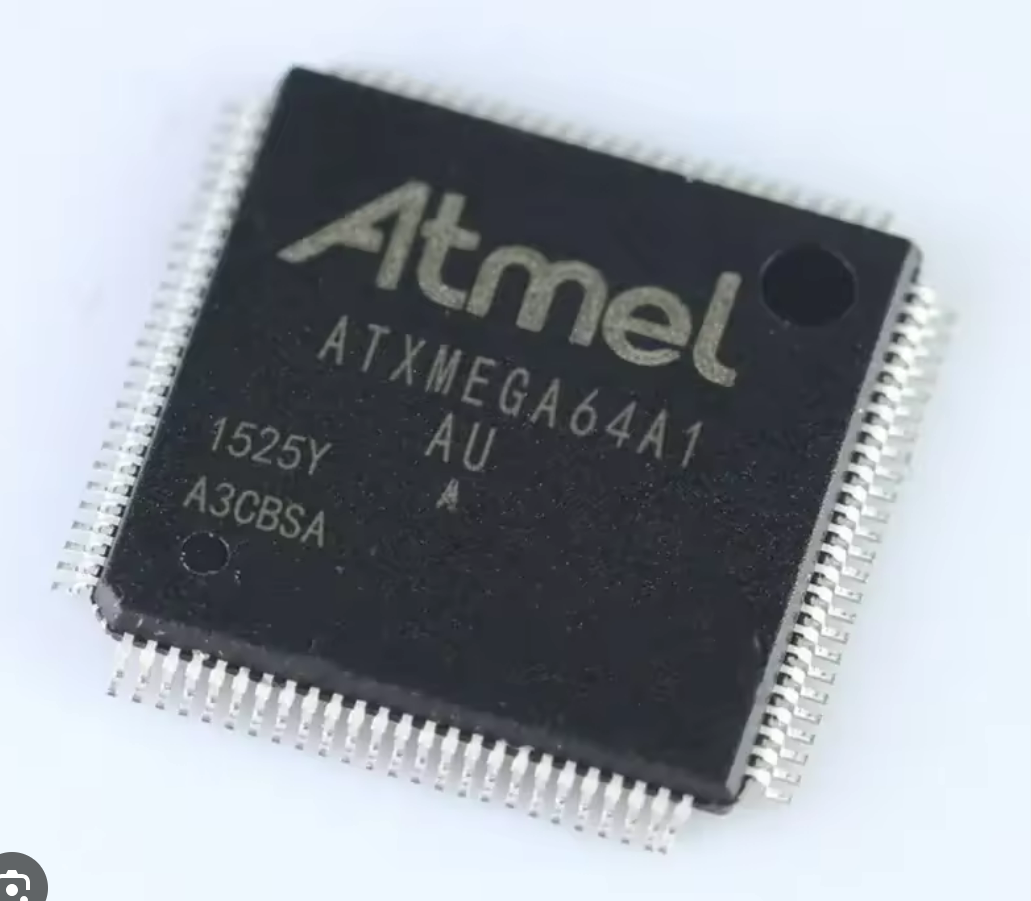
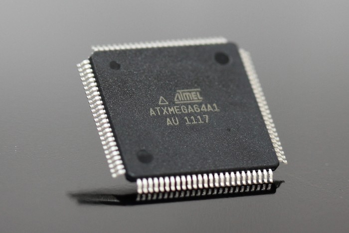
Break MCU ATXMEGA64A1 Heximal
Breaking MCU ATXMEGA64A1 Heximal often involves reverse engineering and decrypting its firmware to access flash memory, EEPROM, or binary code. By analyzing the program’s heximal and binary format, it’s possible to recover, restore, copy, or clone essential software or source code for diagnostics and backup purposes.
Breaking MCU ATXMEGA64A1 Heximal often involves reverse engineering and decrypting its firmware to access flash memory, EEPROM, or binary code. By analyzing the program’s heximal and binary format, it’s possible to recover, restore, copy, or clone essential software or source code for diagnostics and backup purposes
The AVR architecture has two main memory spaces, the Program Memory and the Data Memory. In addition, the XMEGA A1 features an EEPROM Memory for non-volatile data storage after Break MCU ATXMEGA64A1 Heximal.
All three memory spaces are linear and require no paging. The available memory size configurations are shown in “Ordering Information”. In addition each device has a Flash memory signature row for calibration data after Break Microcontroller Samsung S3F9454 Software, device identification, serial number etc. Non-volatile memory spaces can be locked for further write or read/write operations.
la rottura di MCU ATXMEGA64A1 Heximal spesso comporta il reverse engineering e la decifrazione del suo firmware per accedere alla memoria flash, EEPROM o codice binario. Analizzando il formato esadecimale e binario del programma, è possibile recuperare, ripristinare, copiare o clonare software essenziale o codice sorgente per scopi di diagnostica e backup
This prevents unrestricted access to the application software. When the device is powered on, the CPU starts to execute instructions from the lowest address in the Flash Program Memory ‘0’. The Program Counter (PC) addresses the next instruction to be fetched. After a reset, the PC is set to location ‘0’ from MCU Cracking.
Program flow is provided by conditional and unconditional jump and call instructions in order to Break Microcontroller NEC UPD78F0881 Software, capable of addressing the whole address space directly. Most AVR instructions use a 16-bit word format, while a limited number uses a 32-bit format.
غالبًا ما يتضمن كسر MCU ATXMEGA64A1 Heximal الهندسة العكسية وفك تشفير البرامج الثابتة للوصول إلى ذاكرة الفلاش أو EEPROM أو الكود الثنائي. من خلال تحليل تنسيق البرنامج السداسي والثنائي، من الممكن استرداد أو استعادة أو نسخ أو استنساخ البرامج الأساسية أو الكود المصدر لأغراض التشخيص والنسخ الاحتياطي
During interrupts and subroutine calls, the return address PC is stored on the Stack. The Stack is effectively allocated in the general data SRAM, and consequently the Stack size is only limited by the total SRAM size and the usage of the SRAM.
After reset the Stack Pointer (SP) points to the highest address in the internal SRAM. The SP is read/write accessible in the I/O memory space, enabling easy implementation of multiple stacks or stack areas for the purpose of Break Microcontroller TI MSP430F448 Firmware. The data SRAM can easily be accessed through the five different addressing modes supported in the AVR CPU.
• Flash Program Memory
– One linear address space
– In-System Programmable
– Self-Programming and Bootloader support
– Application Section for application code
– Application Table Section for application code or data storage
– Boot Section for application code or bootloader code
– Separate lock bits and protection for all sections
• Data Memory
– One linear address space
– Single cycle access from CPU
– SRAM
– EEPROM
Byte or page accessible
Optional memory mapping for direct load and store
– I/O Memory
Configuration and Status registers for all peripherals and modules
16-bit accessible General Purpose Register for global variables or flags
– External Memory support
– Bus arbitration
Safe and deterministic handling of CPU and DMA Controller priority
– Separate buses for SRAM, EEPROM, I/O Memory and External Memory access
Simultaneous bus access for CPU and DMA Controller
• Calibration Row Memory for factory programmed data
Oscillator calibration bytes
Serial number
Device ID for each device type
• User Signature Row
One flash page in size
Can be read and written from software
Data is kept
злам мікроконтроллера ATXMEGA64A1 Heximal часто передбачає зворотне проектування та розшифровку мікропрограми для доступу до флеш-пам’яті, EEPROM або двійкового коду. Аналізуючи шістнадцятковий і двійковий формати програми, можна відновити, відновити, скопіювати або клонувати важливе програмне забезпечення або вихідний код для діагностики та резервного копіювання.
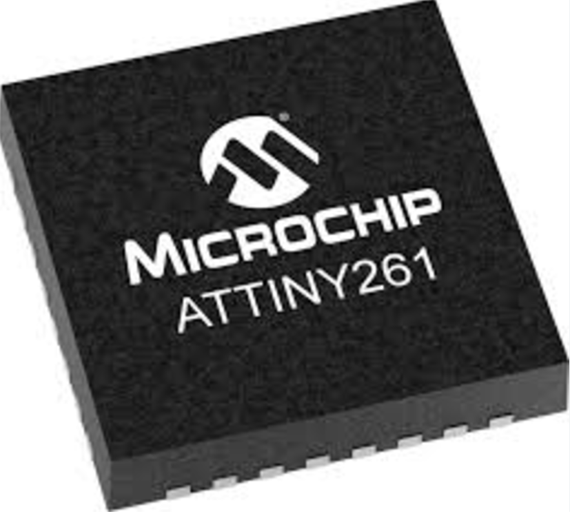
Break IC ATTINY261 Code
Breaking IC ATTINY261 code requires specialized skills to crack or decrypt the secured microcontroller’s encrypted firmware. This protective microcomputer is designed to safeguard its flash memory and EEPROM, storing programs and software in binary or heximal formats. Reverse engineering techniques are often employed to bypass security mechanisms, allowing access to the locked source code for recovery or restoration purposes.
phá mã IC ATTINY261 đòi hỏi các kỹ năng chuyên biệt để bẻ khóa hoặc giải mã chương trình cơ sở được mã hóa của vi điều khiển được bảo mật. Máy vi tính bảo vệ này được thiết kế để bảo vệ bộ nhớ flash và EEPROM của nó, lưu trữ các chương trình và phần mềm ở định dạng nhị phân hoặc thập lục phân. Các kỹ thuật kỹ thuật đảo ngược thường được sử dụng để bỏ qua các cơ chế bảo mật, cho phép truy cập vào mã nguồn bị khóa cho mục đích phục hồi hoặc khôi phục
Professionals may use advanced tools to analyze the encrypted firmware, enabling the cloning or copying of the program stored in the microprocessor. This process demands a deep understanding of the ATTINY261’s architecture, as it is a highly secured MCU with features that protect its code from unauthorized access. Successfully breaking the IC ATTINY261 code enables the recovery of critical data or replication of the firmware for diagnostics or system redundancy. However, it is essential to ensure such actions comply with legal and ethical guidelines.

Break IC ATTINY261 Code
We can Break IC ATTINY261 Code, please view the IC ATTINY261 features for your reference:
High Performance, Low Power AVR® 8-Bit Microcontroller
Advanced RISC Architecture
– 123 Powerful Instructions – Most Single Clock Cycle Execution
– 32 x 8 General Purpose Working Registers
– Fully Static Operation when Break IC
Non-volatile Program and Data Memories
– 2/4/8K Byte of In-System Programmable Program Memory Flash
(ATtiny261/461/861)
Endurance: 10,000 Write/Erase Cycles
– 128/256/512 Bytes In-System Programmable EEPROM (ATtiny261)
Endurance: 100,000 Write/Erase Cycles when Reverse Engineering Microcontroller ATTINY4313 Code
– 128/256/512 Bytes Internal SRAM (ATtiny261/461/861)
– Programming Lock for Self-Programming Flash Program and EEPROM Data Security
Peripheral Features
złamanie kodu IC ATTINY261 wymaga specjalistycznych umiejętności, aby złamać lub odszyfrować zaszyfrowane oprogramowanie układowe zabezpieczonego mikrokontrolera. Ten ochronny mikrokomputer jest zaprojektowany do ochrony pamięci flash i EEPROM, przechowując programy i oprogramowanie w formatach binarnych lub heksametalogowych. Techniki inżynierii wstecznej są często stosowane w celu ominięcia mechanizmów bezpieczeństwa, umożliwiając dostęp do zablokowanego kodu źródłowego w celu odzyskania lub przywrócenia
– 8/16-bit Timer/Counter with Prescaler and Two PWM Channels
– 8/10-bit High Speed Timer/Counter with Separate Prescaler after Break IC ATTINY2313 Code
3 High Frequency PWM Outputs with Separate Output Compare Registers
Programmable Dead Time Generator
– Universal Serial Interface with Start Condition Detector
– 10-bit ADC
11 Single Ended Channels
16 Differential ADC Channel Pairs
15 Differential ADC Channel Pairs with Programmable Gain (1x, 8x, 20x, 32x)
– Programmable Watchdog Timer with Separate On-chip Oscillator if Recover MCU ATTINY45V Program
– On-chip Analog Comparator
Special Microcontroller Features
– debugWIRE On-chip Debug System
– In-System Programmable via SPI Port
– External and Internal Interrupt Sources
– Low Power Idle, ADC Noise Reduction, and Power-down Modes
IC ATTINY261 कोड को तोड़ने के लिए सुरक्षित माइक्रोकंट्रोलर के एन्क्रिप्टेड फर्मवेयर को क्रैक या डिक्रिप्ट करने के लिए विशेष कौशल की आवश्यकता होती है। यह सुरक्षात्मक माइक्रोकंप्यूटर अपनी फ्लैश मेमोरी और EEPROM की सुरक्षा के लिए डिज़ाइन किया गया है, जो प्रोग्राम और सॉफ़्टवेयर को बाइनरी या हेक्सिमल फ़ॉर्मेट में संग्रहीत करता है। रिवर्स इंजीनियरिंग तकनीकों को अक्सर सुरक्षा तंत्र को बायपास करने के लिए नियोजित किया जाता है, जिससे रिकवरी या बहाली के उद्देश्यों के लिए लॉक किए गए स्रोत कोड तक पहुँच की अनुमति मिलती है
– Enhanced Power-on Reset Circuit
– Programmable Brown-out Detection Circuit
– Internal Calibrated Oscillator
I/O and Packages
– 16 Programmable I/O Lines after Break IC
– 20-pin PDIP, 20-pin SOIC and 32-pad MLF
Operating Voltage:
– 1.8 – 5.5V for ATtiny261
– 2.7 – 5.5V for ATtiny261
Speed Grade:
– ATtiny261V/461V/861V: 0 – 4 MHz @ 1.8 – 5.5V, 0 – 10 MHz @ 2.7 – 5.5V when Break IC
– ATtiny261/461/861: 0 – 10 MHz @ 2.7 – 5.5V, 0 – 20 MHz @ 4.5 – 5.5V
– Active Mode: 1 MHz, 1.8V: 380ìA
– Power-down Mode: 0.1ìA at 1.8V
Typical values contained in this data sheet are based on simulations and characterization of other AVR microcontrollers manufactured on the same process technology. Min and Max values will be available after the device is characterized.
The ATtiny261 is a low-power CMOS 8-bit microcontroller based on the AVR enhanced RISC architecture which can facilitate the process of Microcontroller unlocking. By executing powerful instructions in a single clock cycle, the ATtiny261 achieves throughputs approaching 1 MIPS per MHz allowing the system designer to optimize power consumption versus processing speed.
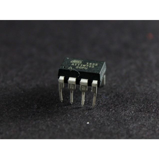
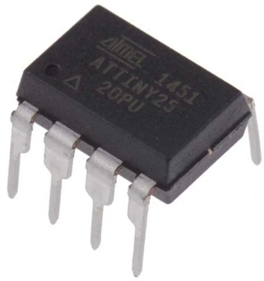
Recover MCU ATTINY25 Flash
Recovering MCU ATTINY25 flash memory involves advanced techniques to crack or decrypt its secured and encrypted firmware. This protective microcomputer is designed with robust security features, making access to its locked flash memory and EEPROM memory a challenging task. Reverse engineering plays a vital role in understanding the microcontroller’s architecture and identifying vulnerabilities that can be exploited to break its protective mechanisms.
Việc khôi phục bộ nhớ flash MCU ATTINY25 liên quan đến các kỹ thuật tiên tiến để bẻ khóa hoặc giải mã chương trình cơ sở được mã hóa và bảo mật của nó. Máy vi tính bảo vệ này được thiết kế với các tính năng bảo mật mạnh mẽ, khiến việc truy cập vào bộ nhớ flash bị khóa và bộ nhớ EEPROM của nó trở thành một nhiệm vụ đầy thách thức. Kỹ thuật đảo ngược đóng vai trò quan trọng trong việc hiểu kiến trúc của bộ vi điều khiển và xác định các lỗ hổng có thể bị khai thác để phá vỡ các cơ chế bảo vệ của nó.
The recovery process often requires specialized hardware and software tools to extract the binary or heximal data stored in the MCU’s memory. By attacking the encrypted security layers, it becomes possible to retrieve the embedded program and source code for restoration or cloning. This can be crucial for system diagnostics, program replication, or firmware backups.
Once the flash memory is successfully accessed, the extracted firmware can be restored to its original functionality or cloned for use in duplicate systems. This process ensures the continuity of operations in cases of hardware failure or program corruption. However, handling such secured microprocessors requires a high level of technical expertise and strict adherence to ethical and legal standards. Unauthorized access to the ATTINY25’s flash memory or software may violate intellectual property rights, emphasizing the importance of responsible and authorized recovery practices.
MCU ATTINY25 फ्लैश मेमोरी को रिकवर करने के लिए इसके सुरक्षित और एन्क्रिप्टेड फर्मवेयर को क्रैक या डिक्रिप्ट करने के लिए उन्नत तकनीकों की आवश्यकता होती है। इस सुरक्षात्मक माइक्रोकंप्यूटर को मजबूत सुरक्षा सुविधाओं के साथ डिज़ाइन किया गया है, जिससे इसकी लॉक की गई फ्लैश मेमोरी और EEPROM मेमोरी तक पहुँचना एक चुनौतीपूर्ण कार्य बन जाता है। रिवर्स इंजीनियरिंग माइक्रोकंट्रोलर की वास्तुकला को समझने और उन कमजोरियों की पहचान करने में महत्वपूर्ण भूमिका निभाती है जिनका उपयोग इसके सुरक्षात्मक तंत्र को तोड़ने के लिए किया जा सकता है।
The ATtiny25 is a low-power CMOS 8-bit mcu based on the AVR enhanced RISC architecture. By executing powerful instructions in a single clock cycle, the ATtiny25 achieves throughputs approaching 1 MIPS per MHz allowing the system designer to optimize power consumption versus processing speed when Recover MCU ATTINY25 Flash.
The AVR core combines a rich instruction set with 32 general purpose working registers. All the 32 registers are directly connected to the Arithmetic Logic Unit (ALU) for the purpose of Copy Microcontroller PIC16F737 Flash, allowing two independent registers to be accessed in one single instruction executed in one clock cycle.
The resulting architecture is more code efficient while achieving throughputs up to ten times faster than conventional CISC mcus.
Recover MCU ATTINY25 Flash
The ATtiny25 provides the following features: 2/4/8K byte of In-System Programmable Flash, 128/256/512 bytes EEPROM, 128/256/256 bytes SRAM, 6 general purpose I/O lines, 32 general purpose working registers, one 8-bit Timer/Counter with compare modes, one 8-bit high speed Timer/Counter, Universal Serial Interface, Internal and External Interrupts, a 4-channel, 10-bit ADC, a programmable Watchdog Timer with internal Oscillator, and three software selectable power saving modes which will facilitate the process of Break Chip PIC16F785 Heximal.
The Idle mode stops the CPU while allowing the SRAM, Timer/Counter, ADC, Analog Comparator, and Interrupt system to continue functioning. The Power-down mode saves the register contents, disabling all chip functions until the next Interrupt or Hardware Reset.
The ADC Noise Reduction mode stops the CPU and all I/O modules except ADC, to minimize switching noise during ADC conversions. The device is manufactured using Atmel’s high density non-volatile memory MCU Crack technology. The On-chip ISP Flash allows the Program memory to be re-programmed In-System through an SPI serial interface after Attack MCU PIC16F636 Binary, by a conventional non-volatile memory programmer or by an On-chip boot code running on the AVR core.
การกู้คืนหน่วยความจำแฟลช MCU ATTINY25 ต้องใช้เทคนิคขั้นสูงในการแคร็กหรือถอดรหัสเฟิร์มแวร์ที่ได้รับการรักษาความปลอดภัยและเข้ารหัส ไมโครคอมพิวเตอร์ป้องกันนี้ได้รับการออกแบบด้วยคุณสมบัติความปลอดภัยที่แข็งแกร่ง ทำให้การเข้าถึงหน่วยความจำแฟลชที่ถูกล็อคและหน่วยความจำ EEPROM เป็นงานที่ท้าทาย วิศวกรรมย้อนกลับมีบทบาทสำคัญในการทำความเข้าใจสถาปัตยกรรมของไมโครคอนโทรลเลอร์และระบุช่องโหว่ที่อาจถูกใช้ประโยชน์เพื่อทำลายกลไกการป้องกัน
The ATtiny25 AVR is supported with a full suite of program and system development tools including: C Compilers, Macro Assemblers, Program Debugger/Simulators, In-Circuit Emulators, and Evaluation kits.
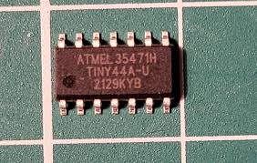
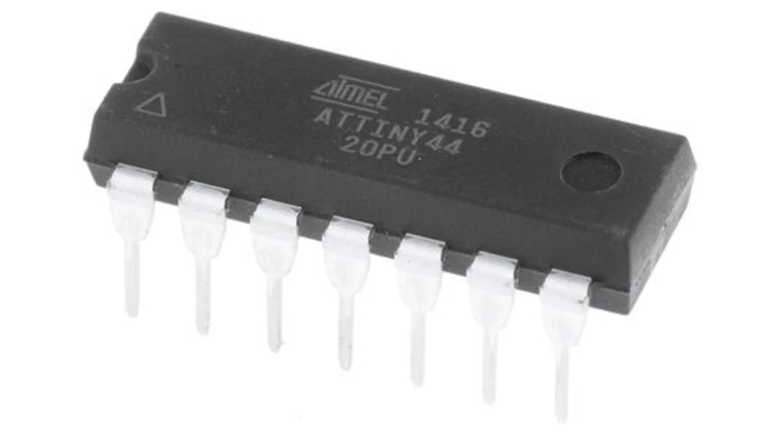
Recover Microcontroller Attiny44 Code
Recovering Microcontroller ATTINY44 code involves advanced techniques to crack and decode its secured and encrypted firmware. This protective microcomputer is designed with robust security features that lock access to its software, source code, and EEPROM memory. Reverse engineering is often required to break through these protective measures, enabling access to the binary or heximal data stored within the MCU.
восстановление кода микроконтроллера ATtiny44 включает в себя передовые методы взлома и декодирования его защищенной и зашифрованной прошивки. Этот защитный микрокомпьютер ATtiny44 разработан с надежными функциями безопасности, которые блокируют доступ к его программному обеспечению, исходному коду и памяти EEPROM. Обратное проектирование часто требуется для взлома этих защитных мер, что позволяет получить доступ к двоичным или шестнадцатеричным данным, хранящимся в микроконтроллере ATtiny44.
The process starts by analyzing the microcontroller’s architecture to unlock its firmware and retrieve the embedded program. Specialized tools are used to decode the secured layers, ensuring the integrity of the recovered code. Once the source code is restored, it can be cloned for legitimate purposes such as hardware replication, software backups, or system diagnostics.
Unlocking a locked microprocessor like the ATTINY44 demands precision and adherence to ethical and legal guidelines, ensuring that recovering, restoring, or cloning its firmware serves authorized and constructive objectives.
Recover Microcontroller Attiny44 Code
We can Recover MCU ATTINY44 Code, please view the MICROCONTROLLER ATTINY44 features for your reference:
EEPROM read from application code does not work in Lock Bit Mode 3
Reading EEPROM when system clock frequency is below 900 kHz may not work, EEPROM read from application code does not work in Lock Bit Mode 3 When the Memory Lock Bits LB2 and LB1 are programmed to mode 3 in order to Attack IC PIC16C74B Binary, EEPROM read does not work from the application code from MCU Cracking. Problem Fix/Work around Do not set Lock Bit Protection Mode 3 when the application code needs to read from EEPROM.
Reading EEPROM when system clock frequency is below 900 kHz may not work Reading data from the EEPROM at system clock frequency below 900 kHz may result in wrong data read. Problem Fix/Work around Avoid using the EEPROM at clock frequency below 900 kHz before Recover Microcontroller Attiny44 Code. Reading EEPROM when system clock frequency is below 900 kHz may not work
Reading EEPROM when system clock frequency is below 900 kHz may not work Reading data from the EEPROM at system clock frequency below 900 kHz may result in wrong data read.
recuperar o código do microcontrolador ATtiny44 envolve técnicas avançadas para quebrar e decodificar seu firmware protegido e criptografado. Este microcomputador protetor ATtiny44 é projetado com recursos de segurança robustos que bloqueiam o acesso ao seu software, código-fonte e memória EEPROM. A engenharia reversa é frequentemente necessária para romper essas medidas de proteção, permitindo o acesso aos dados binários ou hexagonais armazenados dentro do MCU ATtiny44.
Problem Fix/Work around Avoid using the EEPROM at clock frequency below 900 kHz.
Port A is a 8-bit bi-directional I/O port with internal pull-up resistors (selected for each bit). The Port A output buffers have symmetrical drive characteristics with both high sink and source capability. As inputs, Port A pins that are externally pulled low will source current if the pull-up resistors are activated for the purpose of Copy IC PIC12C671 Eeprom. The Port A pins are tri-stated when a reset condition becomes active, even if the clock is not running.
Port A has an alternate functions as analog inputs for the ADC, analog comparator, timer/counter, SPI and pin change interrupt as described in ”Alternate Port Functions”. Port B is a 4-bit bi-directional I/O port with internal pull-up resistors (selected for each bit). The Port B output buffers have symmetrical drive characteristics with both high sink and source capability except PB3 which has the RESET capability to support the process of Copy IC PIC16F884 Code.
تتضمن استعادة شفرة المتحكم الدقيق ATtiny44 تقنيات متقدمة لكسر وفك تشفير البرامج الثابتة المؤمنة والمشفرة. تم تصميم هذا المتحكم الدقيق ATtiny44 الواقي بميزات أمان قوية تغلق الوصول إلى برمجياته ورمزه المصدري وذاكرة EEPROM. غالبًا ما تكون الهندسة العكسية مطلوبة لاختراق هذه التدابير الوقائية، مما يتيح الوصول إلى البيانات الثنائية أو السداسية المخزنة داخل وحدة التحكم الدقيقة ATtiny44.
To use pin PB3 as an I/O pin, instead of RESET pin, program (‘0’) RSTDISBL fuse. As inputs, Port B pins that are externally pulled low will source current if the pull-up resistors are activated. The Port B pins are tri-stated when a reset condition becomes active, even if the clock is not running. Port B also serves the functions of various special features of the ATtiny24/44/84 as listed on Section 12.3 ”Alternate Port Functions” on page 61.
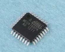
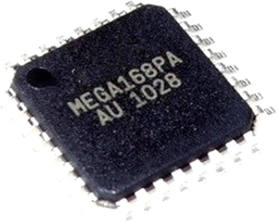
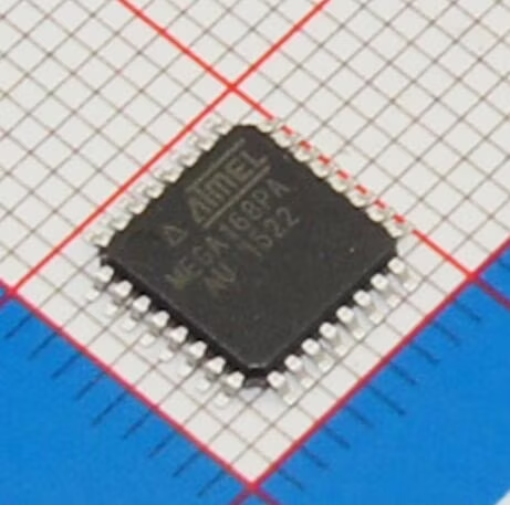
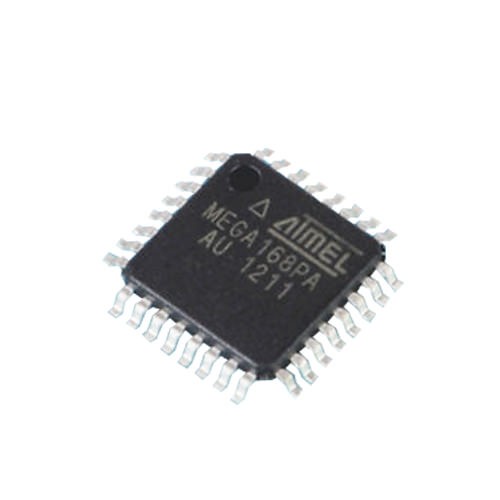
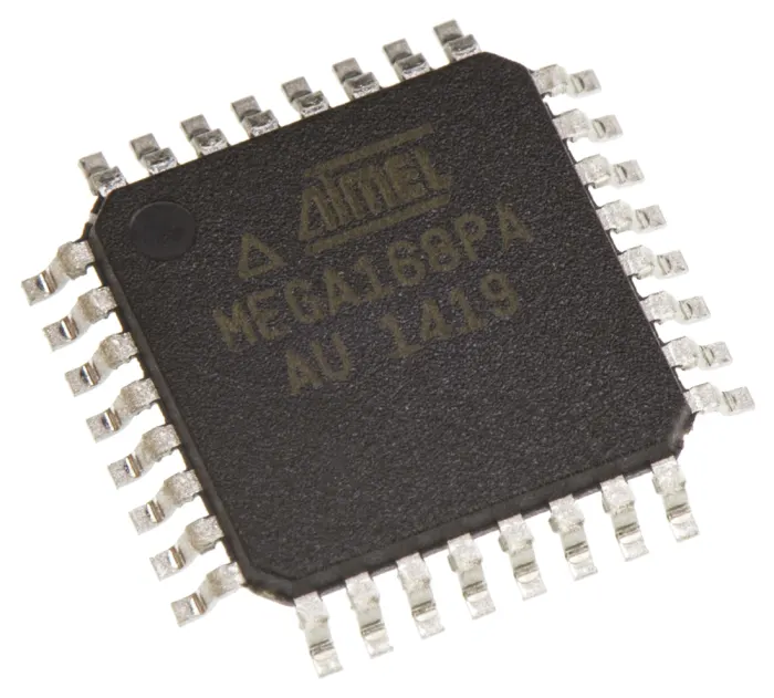
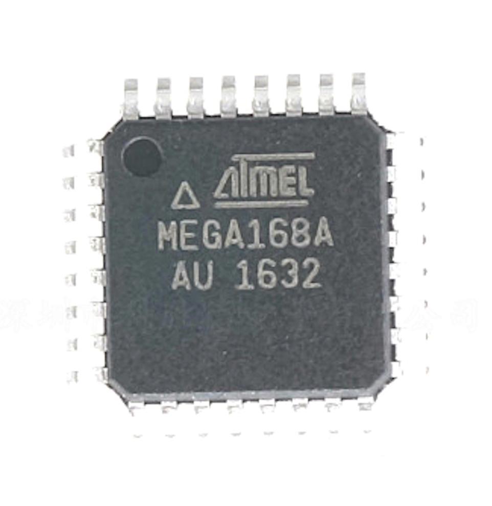
Recover IC ATMEGA168PA Program
Recovering IC ATMEGA168PA program often requires expertise in cracking or decoding its encrypted firmware to access the locked content stored within this secured microcontroller. The ATMEGA168PA, a protective microcomputer, is designed to safeguard its EEPROM memory, firmware, and binary data, ensuring that its program and source code remain protected from unauthorized access. Reverse engineering plays a pivotal role in unlocking its protective mechanisms, allowing professionals to analyze and extract the embedded software.
Recovering IC ATMEGA168PA program often requires expertise in cracking or decoding its encrypted firmware to access the locked content stored within this secured microcontroller. The ATMEGA168PA, a protective microcomputer, is designed to safeguard its EEPROM memory, firmware, and binary data, ensuring that its program and source code remain protected from unauthorized access. Reverse engineering plays a pivotal role in unlocking its protective mechanisms, allowing professionals to analyze and extract the embedded software.
The process typically involves identifying the microcontroller’s encryption layers and using specialized tools to break or bypass its security measures. By decoding the binary or heximal structure of the program, the locked firmware can be accessed and restored for authorized purposes. This may include cloning the firmware to replicate hardware, creating backups, or performing system diagnostics to resolve operational issues.
Unlocking and recovering the program from the IC ATMEGA168PA enables developers to restore lost or corrupted source code, ensuring continued functionality of critical systems. Cloning the secured microprocessor can also provide a reliable backup for future use, safeguarding against potential data loss.
восстановление программы IC ATmega168PA часто требует экспертных знаний по взлому или декодированию ее зашифрованной прошивки для доступа к заблокированному содержимому, хранящемуся в этом защищенном микроконтроллере ATmega168PA. ATMEGA168PA, защитный микрокомпьютер ATmega168PA, разработан для защиты своей памяти EEPROM, прошивки и двоичных данных, гарантируя, что его программа и исходный код остаются защищенными от несанкционированного доступа. Обратное проектирование играет ключевую роль в разблокировке его защитных механизмов, позволяя профессионалам анализировать и извлекать встроенное программное обеспечение.
However, breaking or cracking the protective measures of such an MCU must adhere to ethical and legal guidelines. Unauthorized recovery or cloning of its program could infringe on intellectual property rights, emphasizing the need for responsible practices.

The lowest addresses in the program memory space are by default defined as the Reset and Interrupt Vectors. The complete list of vectors is shown in ”Interrupts” on page 56. The list also determines the priority levels of the different interrupts. The lower the address the higher is the priority level.
RESET has the highest priority, and next is INT0 – the External Interrupt Request; The Interrupt Vectors can be moved to the start of the Boot Flash section by setting the IVSEL bit in the MCU Control Register (MCUCR). Refer to ”Interrupts” on page 56 for more information.
The Reset Vector can also be moved to the start of the Boot Flash section by programming the BOOTRST Fuse, see ”Boot Loader Support – Read-While-Write Self-Programming, ATmega168PA
When an interrupt occurs, the Global Interrupt Enable I-bit is cleared and all interrupts are disabled. The user software can write logic one to the I-bit to enable nested interrupts after breaking off atmega168a secured microcontroller fuse bit. All enabled interrupts can then interrupt the current interrupt routine.
recuperar o programa IC ATmega168PA geralmente requer experiência em quebrar ou decodificar seu firmware criptografado para acessar o conteúdo bloqueado armazenado dentro deste microcontrolador ATmega168PA protegido. O ATMEGA168PA, um microcomputador ATmega168PA protetor, é projetado para proteger sua memória EEPROM, firmware e dados binários, garantindo que seu programa e código-fonte permaneçam protegidos contra acesso não autorizado. A engenharia reversa desempenha um papel fundamental no desbloqueio de seus mecanismos de proteção, permitindo que profissionais analisem e extraiam o software incorporado.
The I-bit is automatically set when a Return from Interrupt instruction – RETI – is executed. There are basically two types of interrupts. The first type is triggered by an event that sets the Interrupt Flag. For these interrupts, the Program Counter is vectored to the actual Interrupt Vector in order to execute the interrupt handling routine, and hardware clears the corresponding Interrupt Flag by Crack MCU Flash.
Interrupt Flags can also be cleared by writing a logic one to the flag bit position(s) to be cleared. If an interrupt condition occurs while the corresponding interrupt enable bit is cleared, the Interrupt Flag will be set and remembered until the interrupt is enabled, or the flag is cleared by software.
attack atmega168pa microcontroller protection and readout heximal file from atmega168pa flash memory and eeprom memory
Similarly, if one or more interrupt conditions occur while the Global Interrupt Enable bit is cleared, the corresponding Interrupt Flag(s) will be set and remembered until the Global Interrupt Enable bit is set, and will then be executed by order of priority.
The second type of interrupts will trigger as long as the interrupt condition is present. These interrupts do not necessarily have Interrupt Flags. If the interrupt condition disappears before the interrupt is enabled, the interrupt will not be triggered.
When the AVR exits from an interrupt, it will always return to the main program and execute one more instruction before any pending interrupt is served. Note that the Status Register is not automatically stored when entering an interrupt routine, nor restored when returning from an interrupt routine to replicate atmega168p avr mcu flash memory content file. This must be handled by software. When using the CLI instruction to disable interrupts, the interrupts will be immediately disabled. No interrupt will be executed after the CLI instruction, even if it occurs simultaneously with the CLI instruction. The following example shows how this can be used to avoid interrupts during the timed EEPROM write sequence.
غالبًا ما يتطلب استرداد برنامج IC ATmega168PA خبرة في كسر أو فك تشفير البرامج الثابتة المشفرة للوصول إلى المحتوى المقفل المخزن داخل متحكم ATmega168PA الآمن هذا. تم تصميم ATMEGA168PA، وهو كمبيوتر ATmega168PA وقائي، لحماية ذاكرة EEPROM والبرامج الثابتة والبيانات الثنائية، مما يضمن حماية برنامجه ورمزه المصدر من الوصول غير المصرح به. تلعب الهندسة العكسية دورًا محوريًا في فتح آليات الحماية الخاصة به، مما يسمح للمحترفين بتحليل واستخراج البرامج المضمنة.
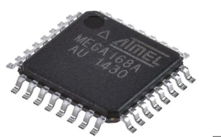
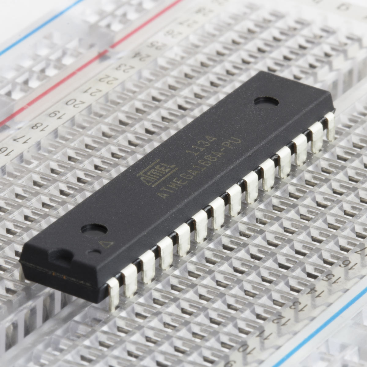
Break MCU ATmega168A Flash
Breaking MCU ATmega168A flash involves cracking the encrypted and locked firmware to access the program and source code embedded within its secured flash memory and EEPROM memory. This protective microcontroller (MCU) is designed to safeguard its binary and heximal data against unauthorized access. However, reverse engineering techniques can be employed to decode and unlock its secured firmware for legitimate purposes such as system restoration or hardware cloning.
Quebrar o flash MCU ATmega168A envolve quebrar o firmware criptografado e bloqueado para acessar o programa e o código-fonte embutidos em sua memória flash segura e memória EEPROM. Este microcontrolador de proteção (MCU) é projetado para proteger seus dados binários e hexagonais contra acesso não autorizado. No entanto, técnicas de engenharia reversa podem ser empregadas para decodificar e desbloquear seu firmware seguro para fins legítimos, como restauração do sistema ou clonagem de hardware.
The process requires an in-depth understanding of the microprocessor’s architecture to bypass security features and retrieve the embedded software. Advanced tools are used to extract and decode the encrypted data stored in the flash memory. Once unlocked, the firmware can be restored to its original functionality or cloned for replication in similar systems.
While breaking the ATmega168A’s flash provides a solution for restoring or replicating old or damaged microcomputers, it must be performed within ethical and legal boundaries to ensure intellectual property rights are respected.
Break MCU ATmega168A Flash
Most of the instructions operating on the Register File have direct access to all registers, and most of them are single cycle instructions. Each register is also assigned a data memory address, mapping them directly into the first 32 locations of the user Data Space. Although not being physically implemented as SRAM locations, this memory organization provides great flexibility in access of the registers which is useful for Break MCU ATmega168A Flash, as the X-, Y- and Z-pointer registers can be set to index any register in the file. The registers R26..R31 have some added functions to their general purpose usage.
These registers are 16-bit address pointers for indirect addressing of the data space. The Stack is mainly used for storing temporary data, for storing local variables and for storing return addresses after interrupts and subroutine calls.
MCU ATmega168A flaşını kırmak, güvenli flaş belleği ve EEPROM belleğinde gömülü programa ve kaynak koduna erişmek için şifrelenmiş ve kilitlenmiş aygıt yazılımını kırmayı içerir. Bu koruyucu mikrodenetleyici (MCU), ikili ve heksimal verilerini yetkisiz erişime karşı korumak için tasarlanmıştır. Ancak, tersine mühendislik teknikleri, sistem geri yükleme veya donanım klonlama gibi meşru amaçlar için güvenli aygıt yazılımını çözmek ve kilidini açmak için kullanılabilir.
The Stack Pointer Register always points to the top of the Stack. Note that the Stack is implemented as growing from higher memory locations to lower memory locations. This implies that a Stack PUSH command decreases the Stack Pointer by Hack IC firmware. The Stack Pointer points to the data SRAM Stack area where the Subroutine and Interrupt Stacks are located. This Stack space in the data SRAM must be defined by the program before any subroutine calls are executed or interrupts are enabled.
The Stack Pointer must be set to point above 0x0100, preferably RAMEND. The Stack Pointer is decremented by one when data is pushed onto the Stack with the PUSH instruction, and it is decremented by two when the return address is pushed onto the Stack with subroutine call or interrupt.
recover embedded firmware from atmega168a mcu flash memory
The Stack Pointer is incremented by one when data is popped from the Stack with the POP instruction, and it is incremented by two when data is popped from the Stack with return from subroutine RET or return from interrupt RETI.
The AVR Stack Pointer is implemented as two 8-bit registers in the I/O space. The number of bits actually used is implementation dependent. Note that the data space in some implementations of the AVR architecture is so small that only SPL is needed. In this case, the SPH Register will not be present after Extract MCU Firmware.
This section describes the general access timing concepts for instruction execution. The AVR CPU is driven by the CPU clock clkCPU, directly generated from the selected clock source for the MCU Cracking. No internal clock division is used.
Figure 5-4 shows the parallel instruction fetches and instruction executions enabled by the Harvard architecture and the fast-access Register File concept. This is the basic pipelining concept to obtain up to 1 MIPS per MHz with the corresponding unique results for functions per cost, functions per clocks, and functions per power-unit.
break ATMEGA168A secured microprocessor fuse bit and readout embedded program from flash memory and data from eeprom memory
The AVR provides several different interrupt sources. These interrupts and the separate Reset Vector each have a separate program vector in the program memory space. All interrupts are assigned individual enable bits which must be written logic one together with the Global Interrupt Enable bit in the Status Register in order to enable the interruption in the process of Break MCU ATmega168A Flash. Depending on the Program Counter value, interrupts may be automatically disabled when Boot Lock bits BLB02 or BLB12 are programmed. This feature improves software security. See the section ”Memory Programming” on page 285 for details.
Взлом флэш-памяти MCU ATmega168A включает взлом зашифрованной и заблокированной прошивки для доступа к программе и исходному коду, встроенному в защищенную флэш-память и память EEPROM. Этот защитный микроконтроллер (MCU) предназначен для защиты своих двоичных и шестнадцатеричных данных от несанкционированного доступа. Однако методы обратного проектирования могут быть использованы для декодирования и разблокировки его защищенной прошивки в законных целях, таких как восстановление системы или клонирование оборудования.
Recovery Microcontroller ATmega48A Program
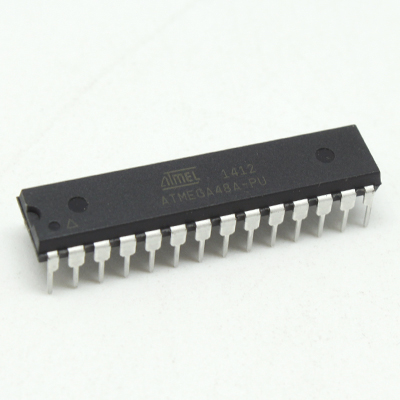
Recovery Microcontroller ATmega48A Program
The Bit Copy instructions BLD (Bit LoaD) and BST (Bit STore) use the T-bit as source or destination for the operated bit. A bit from a register in the Register File can be copied into T by the BST instruction after , and a bit in T can be copied into a bit in a register in the Register File by the BLD instruction.
Bit 5 – H: Half Carry Flag
The Half Carry Flag H indicates a Half Carry in some arithmetic operations. Half Carry Is useful in BCD arithmetic. See the “Instruction Set Description” for detailed information.
Bit 4 – S: Sign Bit, S = N ⊕ V
The S-bit is always an exclusive or between the Negative Flag N and the Two’s Complement Overflow Flag V. See the “Instruction Set Description” for detailed information.
Bit 3 – V: Two’s Complement Overflow Flag
The Two’s Complement Overflow Flag V supports two’s complement arithmetics. See the “Instruction Set Description” for detailed information.
Bit 2 – N: Negative Flag
The Negative Flag N indicates a negative result in an arithmetic or logic operation. See the “Instruction Set Description” for detailed information.
Bit 1 – Z: Zero Flag
The Zero Flag Z indicates a zero result in an arithmetic or logic operation. See the “Instruction Set Description” for detailed information.
Bit 0 – C: Carry Flag
The Carry Flag C indicates a carry in an arithmetic or logic operation. See the “Instruction Set Description” for detailed information.
The Register File is optimized for the AVR Enhanced RISC instruction set in the purpose of Break PIC18F4331 Microprocessor Eeprom Memory. In order to achieve the required performance and flexibility, the following input/output schemes are supported by the Register File:
One 8-bit output operand and one 8-bit result input
Two 8-bit output operands and one 8-bit result input
Two 8-bit output operands and one 16-bit result input
One 16-bit output operand and one 16-bit result input
Figure 5-2 shows the structure of the 32 general purpose working registers in the CPU.
Програма відновлення мікроконтролера ATmega48A передбачає розширені методи злому та декодування зашифрованого та заблокованого мікропрограмного забезпечення, що зберігається в його захищеній флеш-пам’яті та пам’яті EEPROM. Будучи захисним мікроконтролером (MCU), ATmega48A містить надійні функції безпеки для захисту своїх двійкових і шістнадцяткових даних, що робить зворотне проектування необхідним для законних цілей, таких як відновлення функціональності або клонування вбудованого програмного забезпечення.
Most of the instructions operating on the Register File have direct access to all registers, and most of them are single cycle instructions.
Each register is also assigned a data memory address, mapping them directly into the first 32 locations of the user Data Space. Although not being physically implemented as SRAM locations only when Microprocessor PIC18F2515 Heximal File Recovery, this memory organization provides great flexibility in access of the registers, as the X-, Y- and Z-pointer registers can be set to index any register in the file.
The registers R26..R31 have some added functions to their general purpose usage. These registers are 16-bit address pointers for indirect addressing of the data space. The three indirect address registers X, Y, and Z are defined as described in Figure 5-3.
The Stack is mainly used for storing temporary data, for storing local variables and for storing return addresses after interrupts and subroutine calls. The Stack Pointer Register always points to the top of the Stack. Note that the Stack is implemented as growing from higher memory locations to lower memory locations. This implies that a Stack PUSH command decreases the Stack Pointer.
The Stack Pointer points to the data SRAM Stack area where the Subroutine and Interrupt Stacks are located. This Stack space in the data SRAM must be defined by the program before any subroutine calls are executed or interrupts are enabled to provide greater support for Break Microcontroller TI TMS320F28232PGFA Protection. The Stack Pointer must be set to point above 0x0100, preferably RAMEND.
The Stack Pointer is decremented by one when data is pushed onto the Stack with the PUSH instruction, and it is decremented by two when the return address is pushed onto the Stack with subroutine call or interrupt. The Stack Pointer is incremented by one when data is popped from the Stack with the POP instruction, and it is incremented by two when data is popped from the Stack with return from subroutine RET or return from interrupt RETI.
بازیابی میکروکنترلر برنامه ATmega48A شامل روش های پیشرفته ای برای کرک و رمزگشایی سیستم عامل رمزگذاری شده و قفل شده ذخیره شده در حافظه فلش ایمن و حافظه EEPROM است. به عنوان یک میکروکنترلر محافظ (MCU)، ATmega48A دارای ویژگیهای امنیتی قوی برای محافظت از دادههای باینری و هگزیمال خود است، که مهندسی معکوس را برای اهداف قانونی مانند بازیابی عملکرد یا شبیهسازی نرمافزار تعبیهشده ضروری میسازد.
The AVR Stack Pointer is implemented as two 8-bit registers in the I/O space. The number of bits actually used is implementation dependent. Note that the data space in some implementations of the AVR architecture is so small that only SPL is needed when Crack MCU firmware. In this case, the SPH Register will not be present.