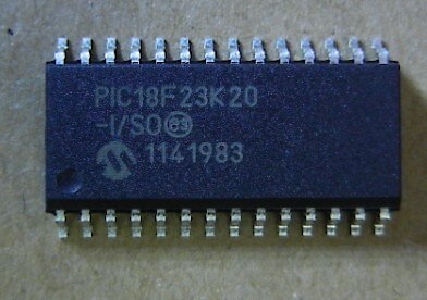
 Recovery Protected Microcontroller PIC18F24K20 Program and Data
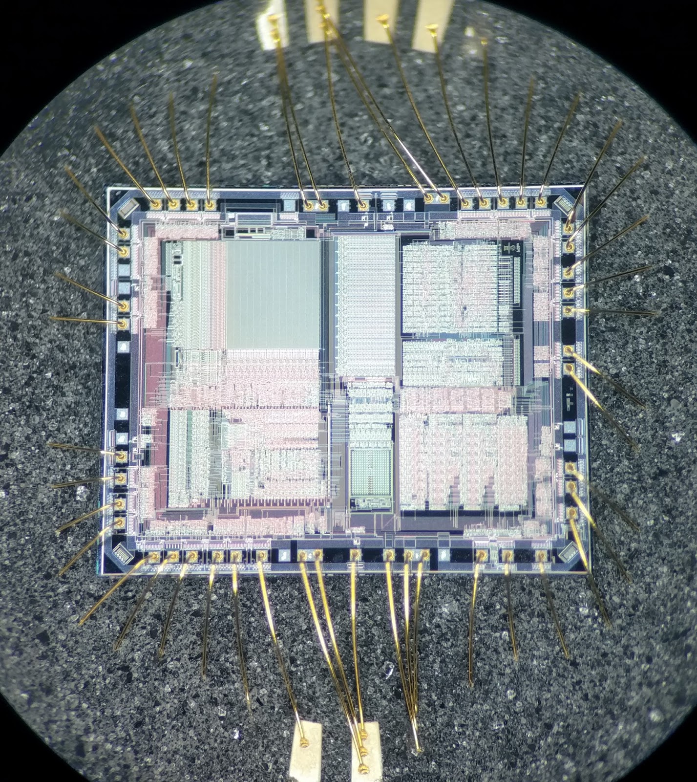
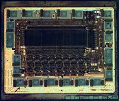
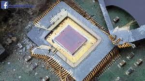
Recovery Protected Microcontroller PIC18F24K20 Program and Data from locked flash and eeprom memory needs to crack pic18f24k20 mcu protective system and disable the tamper resistance, then extract code from IC chip pic18f24k20;
- Memory Endurance: The Flash cells for both program memory and data EEPROM are rated to last for many thousands of erase/write cycles – up to 10K for program memory and 100K for EEPROM. Data retention without refresh is conservatively estimated to be greater than 40 years.
- Self-programmability: These devices can write to their own program memory spaces under inter- nal software control. By using a bootloader rou- tine located in the protected Boot Block at the top of program memory, it becomes possible to create an application that can update itself in the field.

Защищенный микроконтроллер для восстановления PIC18F24K20 встроенной прошивки Данные флэш-памяти и EEPROM из заблокированной флэш-памяти и памяти EEPROM должны взломать защищенный микропроцессор PIC18F24K20 систему защиты от несанкционированного доступа и отключить защиту, затем считывать исходный код в формате двоичного файла или шестнадцатеричных данных с зашифрованных микросхемами PIC18F24K20;
- Extended Instruction Set: The PIC18F2XK20/ 4XK20 family introduces an optional extension to the PIC18 instruction set, which adds 8 new instructions and an Indexed Addressing mode. This extension, enabled as a device configuration option, has been specifically designed to optimize re-entrant application code originally developed in high-level languages, such as C.
- Enhanced CCP module: In PWM mode, this module provides 1, 2 or 4 modulated outputs for controlling half-bridge and full-bridge drivers. Other features include:
- Auto-Shutdown, for disabling PWM outputs on interrupt or other select conditions
- Auto-Restart, to reactivate outputs once the condition has cleared
- Output steering to selectively enable one or more of 4 outputs to provide the PWM signal.
- Enhanced Addressable USART: This serial communication module is capable of standard
recuperação protegida microcontrolador PIC18F24K20 incorporado firmware flash programa e dados eeprom de flash bloqueado e memória eeprom precisa quebrar microprocessador seguro PIC18F24K20 sistema de resistência a violação e desativar a segurança, em seguida, ler o código-fonte no formato de arquivo binário ou dados heximal de microchip criptografado MCU PIC18F24K20;
RS-232 operation and provides support for the LIN bus protocol. Other enhancements include automatic baud rate detection and a 16-bit Baud Rate Generator for improved resolution. When the microcontroller is using the internal oscillator block, the USART provides stable operation for applications that talk to the outside world without using an external crystal (or its accompanying power requirement).
- 10-bit A/D Converter: This module incorporates programmable acquisition time, allowing for a channel to be selected and a conversion to be initiated without waiting for a sampling period and thus, reduce code overhead which can effectively increase the success rate of mcu pic18f4450 memory data recovery.
بازیابی میکروکنترلر محافظت شده PIC18F24K20 برنامه فلش سیستم عامل تعبیه شده و داده های eeprom از فلش قفل شده و حافظه eeprom نیاز به شکستن ریزپردازنده امن PIC18F24K20 سیستم مقاومت در برابر دستکاری و غیر فعال کردن امنیت، سپس کد منبع را در قالب فایل باینری یا داده های هگزیمال از میکروچیپ رمزگذاری شده MCU PIC18F24K20 بخوانید؛
Extended Watchdog Timer (WDT): This enhanced version incorporates a 16-bit postscaler, allowing an extended time-out range that is stable across operating voltage and temperature. See Section 26.0 “Electrical Characteristics” for time-out periods.
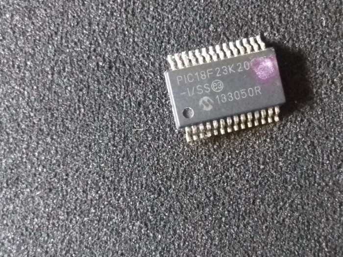
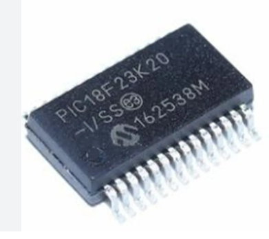
Attack Microchip MCU PIC18F23K20 Memory Unit
Attack Microchip MCU PIC18F23K20 Memory Unit and extract locked heximal from embedded microcontroller after crack microprocessor pic18f23k20 security fuse bit;
All of the devices in the PIC18F23K20 family incorporate a range of features that can significantly reduce power consumption during operation. Key items include:
- Alternate Run Modes: By clocking the controller from the Timer1 source or the internal oscillator block, power consumption during code execution can be reduced by as much as 90%.
- Multiple Idle Modes: The controller can also run with its CPU core disabled but the peripherals still active. In these states, power consumption can be reduced even further, to as little as 4% of normal operation requirements.
atacar o bit de fusível de segurança MCU PIC18F23K20 protegido pela Microchip e extrair dados heximais bloqueados ou arquivo binário da memória de programa flash do microcontrolador PIC18F23K20 incorporado ou memória de dados eeprom;
- On-the-fly Mode Switching: The power- managed modes are invoked by user code during operation, allowing the user to incorporate power- saving ideas into their application’s software design.
- Low Consumption in Key Modules: The power requirements for both Timer1 and the Watchdog Timer are minimized. See Section 26.0 “Electrical Characteristics” for values.
All of the devices in the PIC18F2XK20/4XK20 family offer ten different oscillator options, allowing users a wide range of choices in developing application hardware. These include:
حمله میکروچیپ ایمن MCU PIC18F23K20 بیت فیوز امنیتی و استخراج داده های هگزیمال قفل شده یا فایل باینری از حافظه برنامه فلش میکروکنترلر تعبیه شده PIC18F23K20 یا حافظه داده eeprom.
- Four Crystal modes, using crystals or ceramic resonators
- Two External Clock modes, offering the option of using two pins (oscillator input and a divide-by-4 clock output) or one pin (oscillator input, with the second pin reassigned as general I/O)
- Two External RC Oscillator modes with the same pin options as the External Clock modes
- An internal oscillator block which contains a 16 MHz HFINTOSC oscillator and a 31 kHz LFINTOSC oscillator which together provide 8
user selectable clock frequencies, from 31 kHz to 16 MHz. This option frees the two oscillator pins for use as additional general purpose I/O. A Phase Lock Loop (PLL) frequency multiplier, available to both the high-speed crystal and internal oscillator modes which can be manipulted for breaking microcontroller pic18f14k50 memory, which allows clock speeds of up to 64 MHz.
атаковать микрочип, защищенный битом предохранителя MCU PIC18F23K20, и извлечь заблокированные шестнадцатеричные данные или двоичный файл из встроенной флэш-памяти программ микроконтроллера PIC18F23K20 или памяти данных EEPROM;
Used with the internal oscillator, the PLL gives users a complete selection of clock speeds, from 31 kHz to 64 MHz – all without using an external crystal or clock circuit.
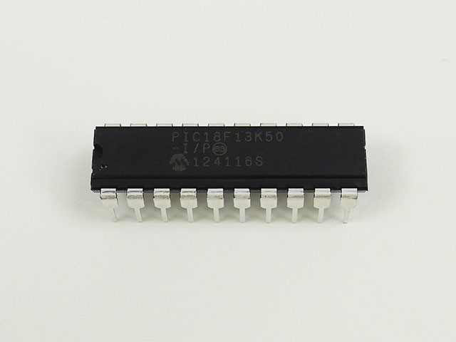
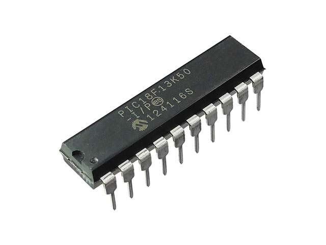
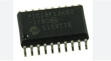
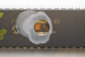
Microcontroller PIC18F13K50 Flash Memory Attacking
Microcontroller PIC18F13K50 Flash Memory Attacking needs to crack pic18f13k50 protective system and read embedded heximal from mcu pic18f13k50;
- Memory Endurance: The Flash cells for both program memory and data EEPROM are rated to last for many thousands of erase/write cycles – up to 1K for program memory and 100K for EEPROM. Data retention without refresh is conservatively estimated to be greater than 40 years which has provide the PIC18F2520 flash binary recovery become possible.
- Self-programmability: These devices can write to their own program memory spaces under internal software control. Using a bootloader routine located in the code protected Boot Block, it is possible to create an application that can update itself in the field.
memória flash do microcontrolador seguro PIC18F13K50 e ataque à memória eeprom precisa quebrar o sistema de proteção do microprocessador PIC18F13K50 e ler o firmware incorporado no formato de dados heximais ou arquivo binário do MCU PIC18F13K50 criptografado;
- Extended Instruction Set: The PIC18(L)F1XK50 family introduces an optional extension to the PIC18 instruction set, which adds eight new instructions and an Indexed Addressing mode. This extension has been specifically designed to optimize re-entrant application code originally developed in high-level languages, such as C.
- Enhanced CCP module: In PWM mode, this module provides 1, 2 or 4 modulated outputs for controlling half-bridge and full-bridge drivers. Other features include:
- Auto-Shutdown, for disabling PWM outputs on interrupt or other select conditions
- Auto-Restart, to reactivate outputs once the condition has cleared
- Output steering to selectively enable one or more of four outputs to provide the PWM signal.
- Enhanced Addressable USART: This serial communication module is capable of standard
میکروکنترلر ایمن فلش مموری PIC18F13K50 و حمله به حافظه eeprom باید سیستم حفاظتی ریزپردازنده PIC18F13K50 را شکسته و سیستم عامل تعبیه شده را در قالب داده هگزیمال یا فایل باینری از MCU رمزگذاری شده PIC18F13K50 بخواند.
RS-232 operation and provides support for the LIN bus protocol. Other enhancements include automatic baud rate detection and a 16-bit Baud Rate Generator for improved resolution.
- 10-bit A/D Converter: This module incorporates programmable acquisition time, allowing for a channel to be selected and a conversion to be initiated without waiting for a sampling period and thus, reduce code overhead.
Extended Watchdog Timer (WDT): This enhanced version incorporates a 16-bit postscaler, allowing an extended time-out range that is stable across operating voltage and temperature.
атака защищенной флэш-памяти микроконтроллера PIC18F13K50 и памяти EEPROM требует взлома защитной системы микропроцессора PIC18F13K50 и считывания встроенной прошивки в формате шестнадцатеричных данных или двоичного файла из зашифрованного MCU PIC18F13K50;
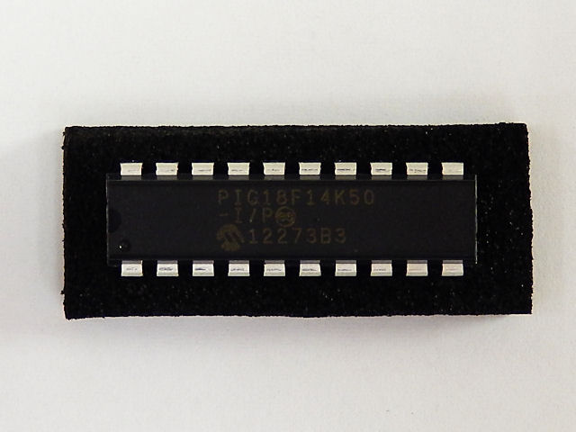
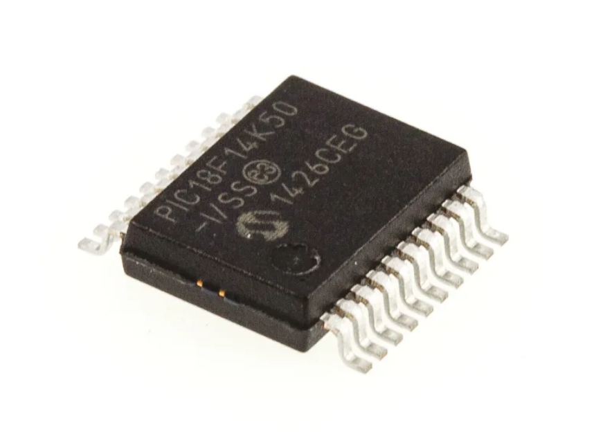
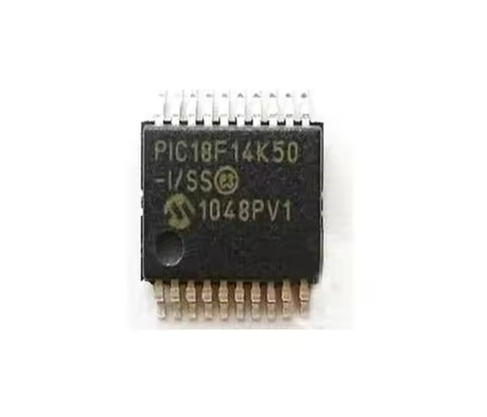
Microchip Processor PIC18F14K50 Flash Memory Breaking
Microchip Processor PIC18F14K50 Flash Memory Breaking is a process to crack pic18f14k50 microcontroller fuse bit and then extract heximal from IC chip memory.
All of the devices in the PIC18(L)F1XK50 family incor- porate a range of features that can significantly reduce power consumption during operation. Key items include:
- Alternate Run Modes: By clocking the controller from the Timer1 source or the internal oscillator block, power consumption during code execution can be reduced by as much as 90%.
- Multiple Idle Modes: The controller can also run with its CPU core disabled but the peripherals still active. In these states, power consumption can be reduced even further, to as little as 4% of normal operation requirements.
- On-the-fly Mode Switching: The power- managed modes are invoked by user code during operation, allowing the user to incorporate power- saving ideas into their application’s software design.
- Low Consumption in Key Modules: The power requirements for both Timer1 and the Watchdog Timer are minimized. See Section 27.0 “Electrical Specifications” for values.
crackear la protección de la memoria del MCU del microchip PIC18F14K50 protegido y recuperar el contenido flash del microcontrolador PIC18F14K50 protegido y el software eeprom de la memoria, copiar datos heximales incorporados o código fuente binario del microprocesador PIC18F14K50 cifrado;
All of the devices in the PIC18(L)F1XK50 family offer ten different oscillator options, allowing users a wide range of choices in developing application hardware. These include:
- Four Crystal modes, using crystals or ceramic resonators
- External Clock modes, offering the option of using two pins (oscillator input and a divide-by-4 clock output) or one pin (oscillator input, with the second pin reassigned as general I/O)
- External RC Oscillator modes with the same pin options as the External Clock modes
- An internal oscillator block which contains a 16 MHz HFINTOSC oscillator and a 31 kHz LFINTOSC oscillator which together provide 8
- user selectable clock frequencies, from 31 kHz to 16 MHz. This option frees the two oscillator pins for use as additional general purpose I/O.
كسر حماية ذاكرة الشريحة الدقيقة PIC18F14K50 MCU واستعادة محتوى الفلاش المحمي PIC18F14K50 وبرنامج eeprom من الذاكرة، ونسخ البيانات السداسية المضمنة أو كود المصدر الثنائي من المعالج الدقيق المشفر PIC18F14K50؛
- A Phase Lock Loop (PLL) frequency multiplier, available to both the high-speed crystal and inter- nal oscillator modes, which allows clock speeds of up to 48 MHz. Used with the internal oscillator, the PLL gives users a complete selection of clock speeds, from 31 kHz to 32 MHz – all without using an external crystal or clock circuit which is a critical flaw for cracking pic18f4550 mcu memory.
Besides its availability as a clock source, the internal oscillator block provides a stable reference source that gives the family additional features for robust operation:
सुरक्षित माइक्रोचिप PIC18F14K50 MCU मेमोरी सुरक्षा को क्रैक करें और मेमोरी से संरक्षित माइक्रोकंट्रोलर PIC18F14K50 फ़्लैश सामग्री और ईप्रोम सॉफ़्टवेयर को पुनर्प्राप्त करें, माइक्रोप्रोसेसर एन्क्रिप्टेड PIC18F14K50 से एम्बेडेड हेक्सिमल डेटा या बाइनरी स्रोत कोड की प्रतिलिपि बनाएँ;
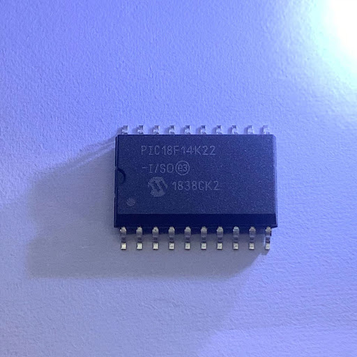
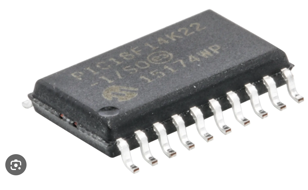
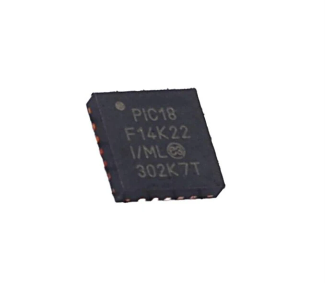
Microchip PIC18F14K22 MCU Flash Memory Breaking
Through our Microchip PIC18F14K22 MCU Flash Memory Breaking technique, engineer can extract embedded heximal from MCU PIC18F14K22 and clone MCU PIC18F14K22 with the same functions;
- Memory Endurance: The Flash cells for both program memory and data EEPROM are rated to last for many thousands of erase/write cycles – up to 10K for program memory and 100K for EEPROM. Data retention without refresh is conservatively estimated to be greater than 40 years.
- Self-programmability: These devices can write to their own program memory spaces under internal software control. Using a bootloader routine located in the code protected Boot Block, it is possible to create an application that can update itself in the field.
La ingeniería inversa de la memoria flash del microcontrolador cifrado PIC18F14K22 es un proceso para descifrar el bit del fusible MCU PIC18F14K22 protegido mediante un haz de iones de enfoque y luego volcar el firmware integrado de la memoria flash PIC18F14K22 del microprocesador bloqueado con microchip y la memoria eeprom en el formato de código fuente heximal o datos de archivos binarios;
- Extended Instruction Set: The PIC18F1XK22/LF1XK22 family introduces an optional extension to the PIC18 instruction set, which adds 8 new instructions and an Indexed Addressing mode. This extension has been spe- cifically designed to optimize re-entrant applica- tion code originally developed in high-level languages, such as C.
- Enhanced CCP module: In PWM mode, this module provides 1, 2 or 4 modulated outputs for controlling half-bridge and full-bridge drivers. Other features include:
- Auto-Shutdown, for disabling PWM outputs on interrupt or other select conditions
- Auto-Restart, to reactivate outputs once the condition has cleared
- Output steering to selectively enable one or more of 4 outputs to provide the PWM signal.
- Enhanced Addressable USART: This serial communication module is capable of standard
रिवर्स इंजीनियरिंग PIC18F14K22 एन्क्रिप्टेड माइक्रोकंट्रोलर फ्लैश मेमोरी फोकस आयन बीम द्वारा संरक्षित MCU PIC18F14K22 फ्यूज बिट को क्रैक करने और फिर हेक्सिमल सोर्स कोड या बाइनरी फ़ाइल डेटा के प्रारूप में माइक्रोचिप लॉक माइक्रोप्रोसेसर PIC18F14K22 फ्लैश मेमोरी और ईप्रोम मेमोरी से एम्बेडेड फर्मवेयर को डंप करने की एक प्रक्रिया है;
RS-232 operation and provides support for the LIN bus protocol. Other enhancements include automatic baud rate detection and a 16-bit Baud Rate Generator for improved resolution.
- 10-bit A/D Converter: This module incorporates programmable acquisition time, allowing for a channel to be selected and a conversion to be initiated without waiting for a sampling period and thus, reduce code overhead which greatly improve the success rate of mcu pic18f2480 program copying.
Extended Watchdog Timer (WDT): This enhanced version incorporates a 16-bit postscaler, allowing an extended time-out range that is stable across operating voltage and temperature. See Section 25.0 “Electrical Specifications” for time-out periods.
الهندسة العكسية ذاكرة فلاش وحدة التحكم الدقيقة المشفرة PIC18F14K22 هي عملية لكسر وحدة MCU PIC18F14K22 المحمية بواسطة شعاع أيون التركيز ثم تفريغ البرامج الثابتة المضمنة من ذاكرة فلاش المعالج الدقيق PIC18F14K22 وذاكرة eeprom بتنسيق كود المصدر السداسي أو بيانات الملف الثنائي؛
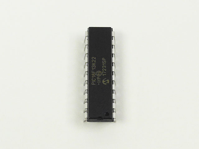
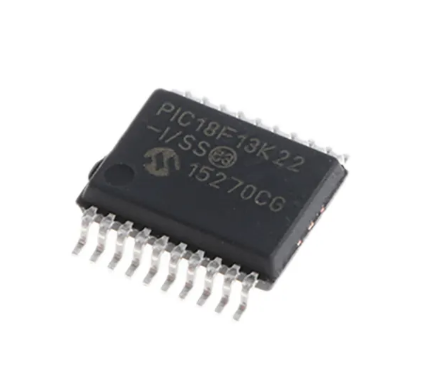
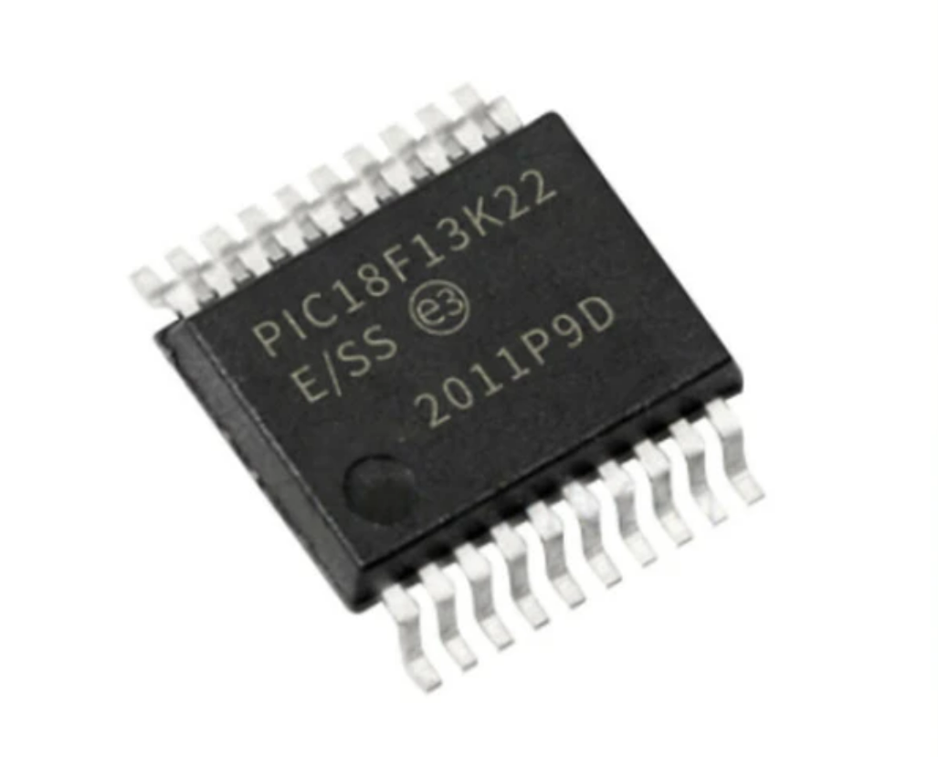
Attack Microchip PIC18F13K22 Microcontroller Flash Memory
Attack Microchip PIC18F13K22 Microcontroller Flash Memory and extract the embedded firmware from microprocessor, the new MCU PIC18F13K22 will be served as MCU cloning units;

This family offers the advantages of all PIC18 microcontrollers – namely, high computational performance with the addition of high-endurance, Flash program memory. On top of these features, the PIC18F13K22 family introduces design enhancements that make these microcontrollers a logical choice for many high-performance, power sensitive applications.
All of the devices in the PIC18F1XK22/LF1XK22 family incorporate a range of features that can significantly reduce power consumption during operation. Key items include:
माइक्रोचिप सुरक्षित PIC18F13K22 माइक्रोकंट्रोलर फ्लैश प्रोग्राम मेमोरी और ईप्रोम डेटा मेमोरी सुरक्षा पर हमला करें, और एन्क्रिप्टेड माइक्रोप्रोसेसर PIC18F13K22 से बाइनरी फ़ाइल या हेक्सिमल सॉफ़्टवेयर के प्रारूप में एम्बेडेड फ़र्मवेयर निकालें, प्रतिकृति के लिए नए MCU माइक्रोचिप PIC18F13K22 में स्रोत कोड की प्रतिलिपि बनाएँ;
- Multiple Idle Modes: The controller can also run with its CPU core disabled but the peripherals still active. In these states, power consumption can be reduced even further, to as little as 4% of normal operation requirements.
- On-the-fly Mode Switching: The
power-managed modes are invoked by user code during operation, allowing the user to incorporate power-saving ideas into their application’s software design to be used for attacking microcontroller pic18f66k90 memory.Low Consumption in Key Modules: The power requirements for both Timer1 and the Watchdog Timer are minimized. See Section 25.0 “Electrical Specifications” for values.
All of the devices in the PIC18F1XK22/LF1XK22 family offer ten different oscillator options, allowing users a wide range of choices in developing application hardware. These include:
- Four Crystal modes, using crystals or ceramic resonators
- External Clock modes, offering the option of using two pins (oscillator input and a divide-by-4 clock output) or one pin (oscillator input, with the sec- ond pin reassigned as general I/O)
- External RC Oscillator modes with the same pin options as the External Clock modes
- An internal oscillator block which contains a 16 MHz HFINTOSC oscillator and a 31 kHz LFINTOSC oscillator which together provide 8
atacar la memoria flash del microcontrolador PIC18F13K22 asegurada por Microchip y la protección de la memoria de datos eeprom, y extraer el firmware integrado en formato de archivo binario o software heximal del microprocesador cifrado PIC18F13K22, copiar el código fuente en el nuevo microchip PIC18F13K22 de MCU para su replicación;
user selectable clock frequencies, from 31 kHz to 16 MHz. This option frees the two oscillator pins for use as additional general purpose I/O.
- A Phase Lock Loop (PLL) frequency multiplier, available to both the high-speed crystal and inter- nal oscillator modes, which allows clock speeds of up to 64 MHz. Used with the internal oscillator, the PLL gives users a complete selection of clock speeds, from 31 kHz to 32 MHz – all without using an external crystal or clock circuit.
Besides its availability as a clock source, the internal oscillator block provides a stable reference source that gives the family additional features for robust operation:
- Fail-Safe Clock Monitor: This option constantly monitors the main clock source against a refer- ence signal provided by the LFINTOSC. If a clock failure occurs, the controller is switched to the internal oscillator block, allowing for continued operation or a safe application shutdown.
attaccare la memoria flash del programma microcontroller PIC18F13K22 protetta da Microchip e la protezione della memoria dati eeprom ed estrarre il firmware incorporato nel formato di file binario o software esimale dal microprocessore crittografato PIC18F13K22, copiare il codice sorgente nel nuovo microchip MCU PIC18F13K22 per la replica;
Two-Speed Start-up: This option allows the internal oscillator to serve as the clock source from Power-on Reset, or wake-up from Sleep mode, until the primary clock source is available.
Attack R5F51306BDFL MCU Flash Memory
Attack Renesas R5F51306BDFL MCU Flash Memory, and extract MCU IC Chip code out from microcontroller flash and eeprom memory, to make the MCU cloning which will provide the same functions;
Below are features of this Flash 32 BIT microcontroller:
Features
- 32-bit RX CPU coreMax. operating frequency: 32 MHz
Capable of 50 DMIPS in operation at 32 MHz
- Accumulator handles 64-bit results (for a single instruction) from 32-bit × 32-bit operations
- Multiplication and division unit handles 32-bit × 32-bit operations (multiplication instructions take one CPU clock cycle)
- Fast interrupt which is also important feature when clone R5F21276 microcontroller firmware
- CISC Harvard architecture with 5-stage pipeline
- Variable-length instructions, ultra-compact code
- On-chip debugging circuit
- Low power design and architecture
- Operation from a single 1.8-V to 5.5-V supply
- Three low power consumption modes
- Low power timer (LPT) that operates during the software standby state
- Supply current
High-speed operating mode: 96 mA/MHz
RENESAS R5F51306BDFL संरक्षित MCU फ्यूज बिट पर हमला करके सुरक्षित माइक्रोकंट्रोलर R5F51306BDFL स्रोत कोड को प्रोग्राम फ्लैश मेमोरी और डेटा eeprom मेमोरी से पुनर्स्थापित करें, बाइनरी फ़ाइल या हेक्सिमल सॉफ़्टवेयर के प्रारूप में स्रोत कोड को नए माइक्रोप्रोसेसर R5F51306BDFL में कॉपी करें;
Supply current in software standby mode: 0.37 mA
- Recovery time from software standby mode: 4.8 ms
- On-chip flash memory for code, no wait states
- Operation at 32 MHz, read cycle of 31.25 ns
- No wait states for reading at full CPU speed
- Programmable at 1.8 V
- For instructions and operands
- On-chip data flash memory
- 8 Kbytes (1,000,000 program/erase cycles (typ.))
- BGO (Background Operation)
- On-chip SRAM, no wait states
- 10- to 16-Kbyte size capacities
- DTC
- Four transfer modes
- Transfer can be set for each interrupt source.
-

atacar el bit de fusible de MCU protegido RENESAS R5F51306BDFL para restaurar el código fuente seguro del microcontrolador R5F51306BDFL desde la memoria flash del programa y la memoria eeprom de datos, copiar el código fuente en formato de archivo binario o software heximal al nuevo microprocesador R5F51306BDFL;
- ELC
- Module operation can be initiated by event signals without using interrupts.
- Linked operation between modules is possible while the CPU is sleeping.
- Reset and supply management
- Eight types of reset, including the power-on reset (POR)
- Low voltage detection (LVD) with voltage settings
- Clock functions
- External clock input frequency: Up to 20 MHz
- Main clock oscillator frequency: 1 to 20 MHz
- Sub clock oscillator frequency: 32.768 kHz
- PLL circuit input: 4 MHz to 8 MHz
- Low-speed on-chip oscillator: 4 MHz
- High-speed on-chip oscillator: 32 MHz ± 1 %
- IWDT-dedicated on-chip oscillator: 15 kHz
- Generate a 32.768 kHz clock for the real-time clock
- On-chip flash memory for code, no wait states
attaccare il bit del fusibile MCU protetto RENESAS R5F51306BDFL per ripristinare il codice sorgente protetto del microcontrollore R5F51306BDFL dalla memoria flash del programma e dalla memoria eeprom dei dati, copiare il codice sorgente nel formato di file binario o software esimale sul nuovo microprocessore R5F51306BDFL;
On-chip clock frequency accuracy measurement circuit (CAC)
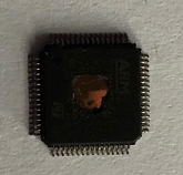
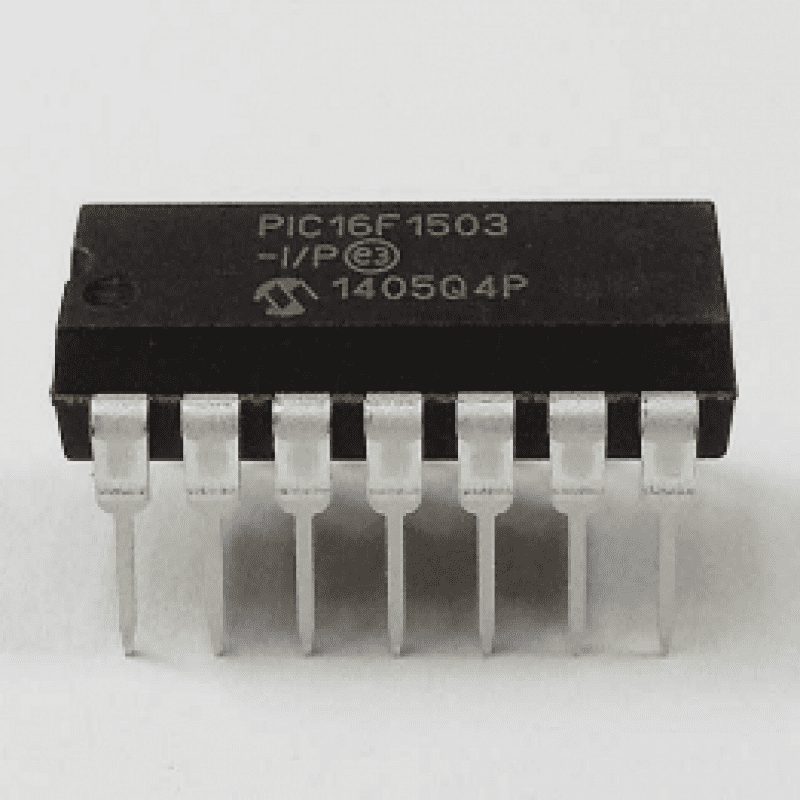
Reverse PIC16F1503 Microchip Controller Memory
Reverse PIC16F1503 Microchip Controller Memory can effectively find a way to locate the security fuse bit through crack MCU protection and extract the embedded firmware hex from pic16f1503 flash memory;
This family of devices contain an enhanced mid-range 8-bit CPU core. The CPU has 49 instructions. Interrupt capability includes automatic context saving. The hardware stack is 16 levels deep and has Overflow and Underflow Reset capability. Direct, Indirect, and Relative addressing modes are available. Two File Select Registers (FSRs) provide the ability to recover PIC16f628 mcu program and data memory.
الهندسة العكسية لوحدة التحكم الدقيقة المؤمنة PIC16F1503 واستعادة البرامج الثابتة المضمنة يمكن أن تجد بشكل فعال طريقة لتحديد موقع بت فتيل الأمان من خلال تشفير MCU PIC16F1503 الواقي من الكراك واستخراج الملف السداسي أو البيانات الثنائية من المعالج الدقيق المشفر ذاكرة فلاش PIC16F1503 أو ذاكرة eeprom؛
- Automatic Interrupt Context Saving
- 16-level Stack with Overflow and Underflow
- File Select Registers
- Instruction Set
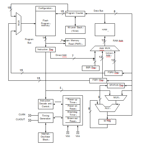
During interrupts, certain registers are automatically saved in shadow registers and restored when returning from the interrupt. This saves stack space and user code.
These devices have a hardware stack memory 15 bits wide and 16 words deep. A Stack Overflow or Under- flow will set the appropriate bit (STKOVF or STKUNF) in the PCON register, and if enabled, will cause a soft- ware Reset.
There are two 16-bit File Select Registers (FSR). FSRs can access all file registers and program mem- ory, which allows one Data Pointer for all memory. When an FSR points to program memory, there is one additional instruction cycle in instructions using INDF to allow the data to be fetched.
مهندسی معکوس PIC16F1503 میکروکنترلر ایمن شده با ریزتراشه و بازیابی سیستم عامل تعبیه شده می تواند به طور موثر راهی برای تعیین محل بیت فیوز امنیتی از طریق رمزگذاری محافظ کرک MCU PIC16F1503 پیدا کند و فایل هگزیمال یا داده های باینری را از ریزپردازنده رمزگذاری شده PIC16F1503 حافظه فلش استخراج کند.
General purpose memory can now also be addressed linearly, providing the ability to access contiguous data larger than 80 bytes. There are also new instructions to support the FSRs when extract code from pic16f1507 microchip memory. There are 49 instructions for the enhanced mid-range CPU to support the features of the CPU.

रिवर्स इंजीनियरिंग PIC16F1503 माइक्रोचिप सुरक्षित माइक्रोकंट्रोलर और बहाल एम्बेडेड फर्मवेयर प्रभावी ढंग से दरार सुरक्षात्मक MCU PIC16F1503 एन्क्रिप्शन के माध्यम से सुरक्षा फ्यूज बिट का पता लगाने और एन्क्रिप्टेड माइक्रोप्रोसेसर PIC16F1503 फ्लैश मेमोरी या eeprom मेमोरी से हेक्सिमल फ़ाइल या बाइनरी डेटा निकालने का एक तरीका पा सकते हैं;
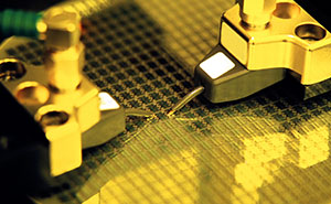
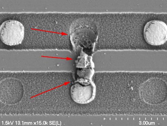
Break dsPIC30F5016 Microchip MCU Flash Memory
Break dsPIC30F5016 Microchip MCU Flash Memory needs to Crack MCU dsPIC30F5016 security fuse bit and extract locked program from microcontroller dsPIC30F5016 flash and eeprom memory;
The core has a 24-bit instruction word. The Program Counter (PC) is 23 bits wide with the Least Significant bit (LSb) always clear (see Section 3.1 “Program Address Space”), and the Most Significant bit (MSb) is ignored during normal program execution, except for certain specialized instructions. Thus, the PC can address up to 4M instruction words of user program space.
كسر حماية نظام مقاومة العبث dsPIC30F5016 Microchip MCU واستعادة برنامج ذاكرة الفلاش بالإضافة إلى بيانات ذاكرة eeprom التي تحتاج إلى كسر وحدة التحكم الدقيقة الآمنة dsPIC30F5016 بت فتيل الأمان ونسخ الملف الثنائي المقفل أو الكود السداسي من المعالج الدقيق المضمون dsPIC30F5016؛
An instruction prefetch mechanism is used to help maintain throughput. Program loop constructs, free from loop count management overhead, are supported using the DO and REPEAT instructions, both of which are interruptible at any point to break PIC16F917 MCU memory. The working register array consists of 16×16-bit registers, each of which can act as data, address or offset registers. One working register (W15) operates as a software Stack Pointer for interrupts and calls.
dsPIC30F5016 محافظ میکروچیپ MCU سیستم مقاومت در برابر دستکاری و بازیابی برنامه فلش مموری به علاوه داده های حافظه eeprom نیاز به کرک کردن بیت فیوز امنیتی میکروکنترلر ایمن dsPIC30F5016 و کپی کردن فایل باینری قفل شده یا کد هگزیمال از dsPIC30F5016 ایمن شده با میکروپروسسور دارد.
The data space is 64 Kbytes (32K words) and is split into two blocks, referred to as X and Y data memory. Each block has its own independent Address Generation Unit (AGU). Most instructions operate solely through the X memory AGU, which provides the appearance of a single unified data space. The Multiply-Accumulate (MAC) class of dual source DSP instructions operate through both the X and Y AGUs, splitting the data address space into two parts (see Section 3.2 “Data Address Space”). The X and Y data space boundary is device specific and cannot be altered by the user.
सुरक्षात्मक dsPIC30F5016 माइक्रोचिप MCU छेड़छाड़ प्रतिरोध प्रणाली को तोड़ने और फ्लैश मेमोरी कार्यक्रम प्लस eeprom स्मृति डेटा को पुनर्प्राप्त करने के लिए सुरक्षित माइक्रोकंट्रोलर dsPIC30F5016 सुरक्षा फ्यूज बिट को तोड़ने और माइक्रोप्रोसेसर सुरक्षित dsPIC30F5016 से लॉक बाइनरी फ़ाइल या हेक्सिमल कोड की प्रतिलिपि बनाने की आवश्यकता है;
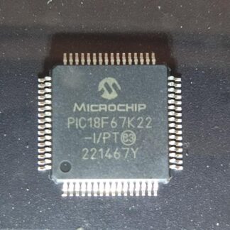
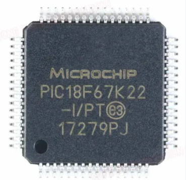
Attack PIC18F67K22 Microcontroller Memory
Attack PIC18F67K22 Microcontroller Memory can help engineer to disable the protection of MCU, and embedded binary from PIC18F67K22 MCU will be unlocked and extracted;
All of the devices in the PIC18F67K22 family offer different oscillator options, allowing users a range of choices in developing application hardware. These include:
· A Phase Lock Loop (PLL) frequency multiplier, available to the external oscillator modes which allows clock speeds of up to 64 MHz. PLL can also be used with the internal oscillator.
· An internal oscillator block that provides a 16 MHz clock (±2% accuracy) and an INTRC source (approximately 31 kHz, stable over temperature and VDD)
The PIC18F67K22 family provides ample room for application code, from 32 Kbytes to 128 Kbytes of code space. The Flash cells for program memory are rated to last up to 10,000 erase/write cycles. Data retention without refresh is conservatively estimated to be greater than 40 years.
saldırı şifreli MICROCHIP PIC18F67K22 mikrodenetleyici flash belleği ve eeprom belleği, mühendisin koruyucu PIC18F67K22 MCU’nun korumasını devre dışı bırakmasına yardımcı olabilir ve orijinal ana mikroişlemci PIC18F67K22’den gelen ikili dosyanın veya onaltılık verilerin gömülü aygıt yazılımının kilidi açılacak ve çıkarılacaktır;
The Flash program memory is readable and writable. During normal operation, the PIC18F87K22 family also provides plenty of room for dynamic application data with up to 3,862 bytes of data RAM. Should 128 Kbytes of memory be inadequate for an application, the 80-pin members of the PIC18F87K22 family have an External Memory Bus (EMB) enabling the controller’s internal program counter to address a memory space of up to 2 Mbytes. This is a level of data access that few 8-bit devices can claim and enables:
атака зашифрованная флэш-память микроконтроллера MICROCHIP PIC18F67K22 и память EEPROM могут помочь инженеру отключить защиту защитного микроконтроллера PIC18F67K22, а встроенная прошивка двоичного файла или шестнадцатеричных данных из исходного главного микропроцессора PIC18F67K22 будет разблокирована и извлечена;
The PIC18F67K22 family implements the optional extension to the PIC18 instruction set, adding eight new instructions and an Indexed Addressing mode. Enabled as a device configuration option, the extension has been specifically designed to optimize re-entrant application code originally developed in high-level languages, such as ‘C’.
ataque criptografado à memória flash do microcontrolador MICROCHIP PIC18F67K22 e à memória eeprom pode ajudar o engenheiro a desativar a proteção do MCU protetor PIC18F67K22, e o firmware incorporado do arquivo binário ou dados heximais do microprocessador mestre original PIC18F67K22 será desbloqueado e extraído;