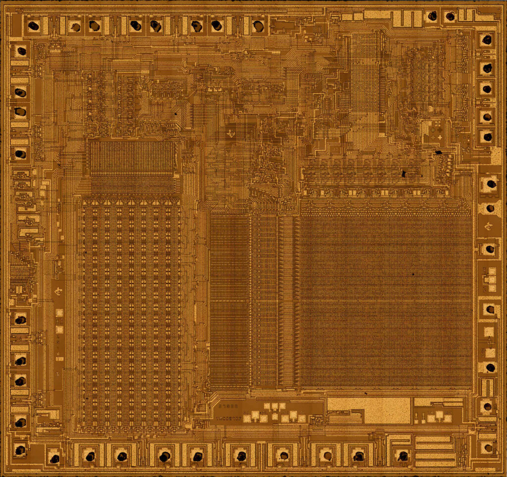
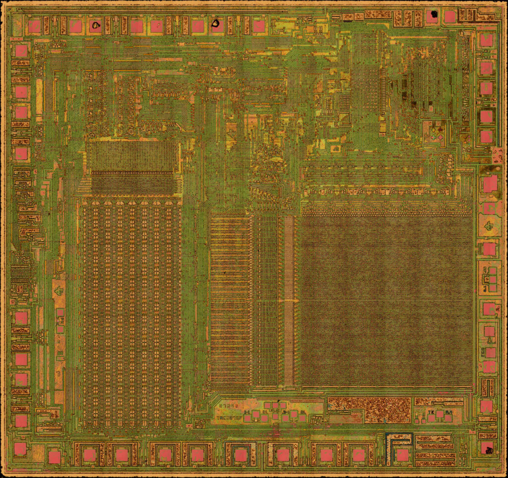
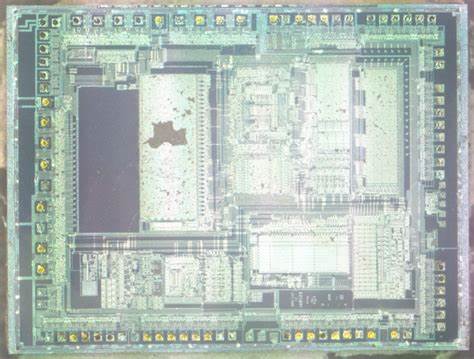
 Reverse Engineering TMS320F28016 Microprocessor Flash Code
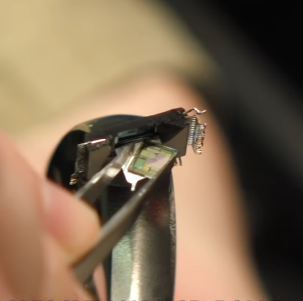
Reverse Engineering TMS320F28016 Microprocessor Flash Firmware is a process to unlock tms320f28016 dsp mcu security fuse bit, then extract embedded source code from microcontroller;
Interface to memory and I/O devices of varying speeds is accomplished by using the READY input. When transactions are made with slower devices, the TMS320F28016 processor waits until the other device completes its function and signals the processor by way of the READY input.
Once a ready indication is provided from the external device, execution continues. On the ’x240 device, the READY input must be driven (active high) to complete reads or writes to internal data I/O-memory-mapped registers and all external addresses only.
The bus request (BR) signal is used in conjunction with the other TMS320F28016 interface signals to arbitrate external global-memory accesses. Global memory is external data-memory space in which the BR signal is asserted at the beginning of the access.
When an external global-memory device receives the bus request, it responds by asserting the ready signal after the global-memory access is arbitrated and the global access is completed.
The TMS320F28016 supports zero-wait-state reads on the external interface. However, to avoid bus conflicts, writes take two cycles. This allows the ’x240 to buffer the transition of the data bus from input to output (or output to input) by a half cycle by breaking mcu tms320f28021 mcu memory. In most systems, TMS320F28016 ratio of reads to writes is significantly large to minimize the overhead of the extra cycle on writes.
Wait states can be generated when accessing slower external resources. The wait states operate on machine-cycle boundaries and are initiated either by using the ready signal or using the software wait-state generator to recover microcontroller tms320f28012pgfa firmware. Ready can be used to generate any number of wait states.
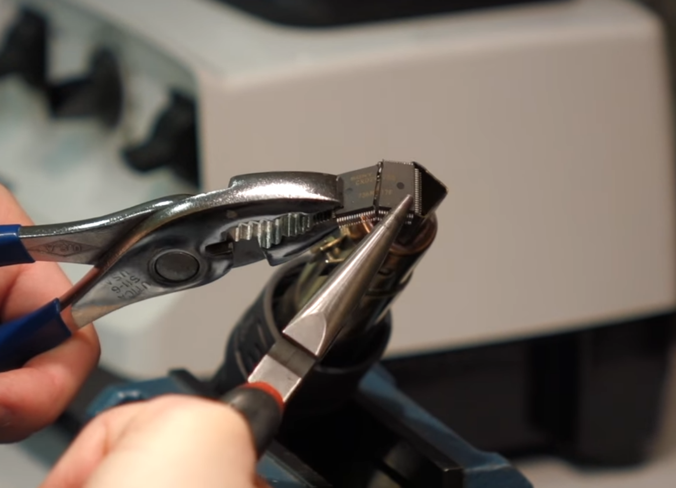
TI DSP MCU TMS320F28015 Program Recovering
TI DSP MCU TMS320F28015 Program Recovering is a process to crack microcontroller tms320f28015 protection and readout MCU embedded firmware from flash memory;
The TMS320F28015 devices include the four-pin serial peripheral interface (SPI) module. The SPI is a high-speed synchronous serial-I/O port that allows a serial bit stream of programmed length in the process of attacking DSP Microcontroller TMS320F28232PGFA (one to eight bits) to be shifted into and out of the device at a programmable bit-transfer rate.
Normally, the SPI is used for communications between the DSP controller and external peripherals or another processor. Typical applications include external I/O or peripheral expansion through devices such as shift registers, display drivers, and ADCs. Multidevice communications are supported by the master/slave operation of the SPI.
The SPI module features include the following:
Four external pins:
- SPISOMI: SPI slave-output/master-input pin, or general-purpose bidirectional I/O pin
- SPISIMO: SPI slave-input/master-output pin, or general-purpose bidirectional I/O pin
- SPISTE: SPI slave-transmit-enable pin, or general-purpose bidirectional I/O pin
- SPICLK: SPI serial-clock pin, or general-purpose bidirectional I/O pin
Two operational modes: master and slave
Baud rate: 125 different programmable rates / 2.5 Mbps at 10-MHz SYSCLK
Data word format: one to eight data bits
Four clocking schemes controlled by clock polarity and clock-phase bits include:
Falling edge without phase delay: SPICLK active high. SPI transmits data on the falling edge of the SPICLK signal and receives data on the rising edge of the SPICLK in order to Crack Locked MCU TMS320F28069 Flash
Falling edge with phase delay: SPICLK active high. SPI transmits data one half-cycle ahead of the falling edge of the SPICLK signal and receives data on the falling edge of the SPICLK
Rising edge without phase delay: SPICLK inactive SPI transmits data on the rising edge of the SPICLK signal and receives data on the falling edge of the SPICLK signal to Reverse Engineering Microcontroller.
Rising edge with phase delay: SPICLK inactive SPI transmits data one half-cycle ahead of the falling edge of the SPICLK signal and receives data on the rising edge of the SPICLK signal.
Simultaneous receive and transmit operations to facilitate the progress (transmit function can be disabled in software)
Transmitter and receiver operations are accomplished through either interrupt-driven or polled algorithms.
Ten SPI module control registers: Located in control register frame beginning at address 7040h.
NOTE: All registers in this module are 8-bit registers that are connected to the 16-bit peripheral bus. When a register is accessed, the register data is in the lower byte (7 – 0), and the upper byte (15 – 8) is read as zeros. Writing to the upper byte has no effect.
Break Microchip PIC18F44K22 Controller Flash Memory
Break Microchip PIC18F44K22 Controller Flash Memory and crack mcu pic18f44k22 protective system then readout embedded firmware fro microcontroller;
The external Resistor-Capacitor (RC) modes support the use of an external RC circuit. This allows the designer maximum flexibility in frequency choice while keeping costs to a minimum when clock accuracy is not required. There are two modes: RC and RCIO.
In RC mode, the RC circuit connects to OSC1. OSC2/ CLKOUT outputs the RC oscillator frequency divided by 4. This signal may be used to provide a clock for external circuitry in order to faciliate the process of breaking microchip mcu pic18f14k22 flash memory, synchronization, calibration, test or other application requirements. Figure 2-8 shows the external RC mode connections.
In RCIO mode, the RC circuit is connected to OSC1. OSC2 becomes a general purpose I/O pin.
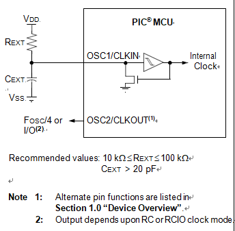
The RC oscillator frequency is a function of the supply voltage, the resistor (REXT) and capacitor (CEXT) values and the operating temperature. Other factors affecting the oscillator frequency are:
- input threshold voltage variation
- component tolerances
- packaging variations in capacitance
The user also needs to take into account variation due to tolerance of external RC components used.
Duplicating Microchip PIC18F43K22 MCU Flash Program
Duplicating Microchip PIC18F43K22 MCU Flash Program needs to crack microcontroller pic18f43k22 security fuse bit and extract encrypted code from microprocessor.
The LP, XT and HS modes support the use of quartz crystal resonators or ceramic resonators connected to OSC1 and OSC2 (Figure 2-6). The mode selects a low, medium or high gain setting of the internal inverter- amplifier to support various resonator types and speed.
LP Oscillator mode selects the lowest gain setting of the internal inverter-amplifier. LP mode current consumption is the least of the three modes. This mode is best suited to drive resonators with a low drive level specification, for example, tuning fork type crystals.
XT Oscillator mode selects the intermediate gain setting of the internal inverter-amplifier. XT mode current consumption is the medium of the three modes. This mode is best suited to drive resonators with a medium drive level specification.HS Oscillator mode offers a Medium Power (MP) and a High Power (HP) option selectable by the FOSC<3:0> bits.
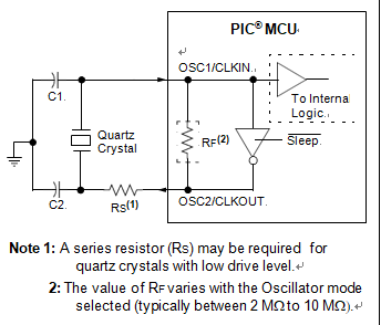
The MP selections are best suited for oscillator frequencies between 4 and 16 MHz. The HP selection has the highest gain setting of the internal inverter- amplifier and is best suited for frequencies above 16 MHz when hacking microchip mcu pic18f26k80 secured flash. HS mode is best suited for resonators that require a high drive setting.
Attack Microchip MCU PIC18F26K22 Flash Memory
Attack Microchip MCU PIC18F26K22 Flash Memory and make pic18f26k22 microcontroller cloning unit after copy embedded heximal from flash memory to new MCU unit.

The IDLEN bit of the OSCCON register determines whether the device goes into Sleep mode or one of the Idle modes when the SLEEP instruction is executed.
Clock Source modes can be classified as external or internal.
- External Clock modes rely on external circuitry for the clock source. Examples are: Clock modules (EC mode), quartz crystal resonators or ceramic resonators (LP, XT and HS modes) and Resistor- Capacitor (RC mode) circuits.
- Internal clock sources are contained internally within the Oscillator block. The Oscillator block has three internal oscillators: the 16 MHz High- Frequency Internal Oscillator (HFINTOSC), 500 kHz Medium-Frequency Internal Oscillator
(MFINTOSC) and the 31.25 kHz Low-Frequency Internal Oscillator (LFINTOSC). The system clock can be selected between external or internal clock sources via the System Clock Select (SCS<1:0>) bits of the OSCCON register. See Section 2.9 “Clock Switching”for additional information by reversing pic18f25k20 mcu locked heximal.
attacco Microchip MCU PIC18F26K22 memoria flash e ripristinare PIC18F26K22 unità di clonazione del microcontrollore dopo aver estratto il firmware incorporato e il codice sorgente, inclusi i dati esamidali e il programma binario dalla memoria flash e dalla memoria eeprom per il reverse engineering della nuova unità di PIC18F26K22 del microprocessore
When the oscillator module is configured for LP, XT or HS modes, the Oscillator Start-up Timer (OST) counts 1024 oscillations from OSC1. This occurs following a Power-on Reset (POR) and when the Power-up Timer (PWRT) has expired (if configured), or a wake-up from Sleep.
atak Microchip MCU PIC18F26K22 pamięć flash i przywracanie jednostki klonowania mikrokontrolera PIC18F26K22 po wyodrębnieniu wbudowanego oprogramowania układowego i kodu źródłowego, w tym danych szesnastkowych i programu binarnego z pamięci flash i pamięci EEPROM w celu inżynierii wstecznej nowej jednostki PIC18F26K22 mikroprocesora
During this time, the program counter does not increment and program execution is suspended. The OST ensures that the oscillator circuit, using a quartz crystal resonator or ceramic resonator, has started and is providing a stable system clock to the oscillator module by duplicating microchip pic18f26k20 source code. When switching between clock sources, a delay is required to allow the new clock to stabilize.
مهاجمة Microchip MCU PIC18F26K22 ذاكرة فلاش واستعادة وحدة استنساخ متحكم PIC18F26K22 بعد استخراج البرامج الثابتة المضمنة وشفرة المصدر بما في ذلك البيانات السداسية والبرنامج الثنائي من ذاكرة الفلاش وذاكرة EEPROM لعكس الهندسة الجديدة وحدة PIC18F26K22 المعالجات الدقيقة
These oscillator delays are shown in Table 2-2. In order to minimize latency between external oscillator start-up and code execution, the Two-Speed Clock Start-up mode can be selected (see Section 2.10 “Two-Speed Clock Start-up Mode”).
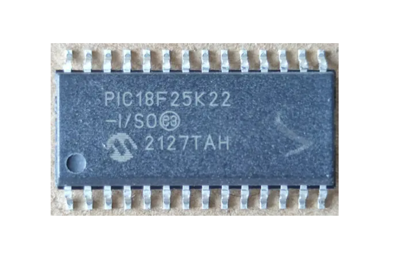
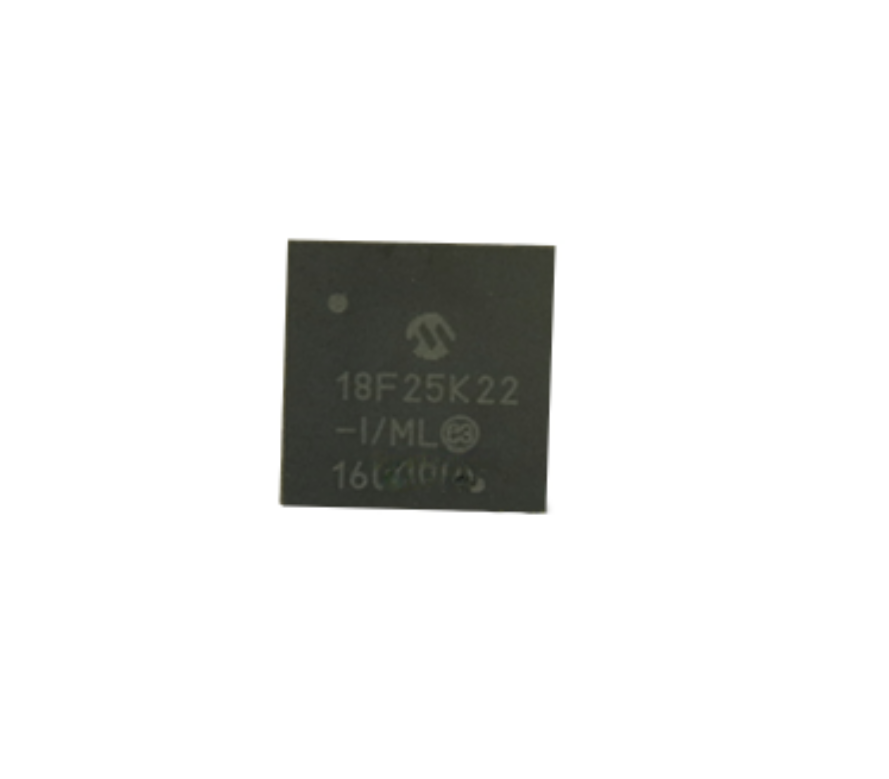
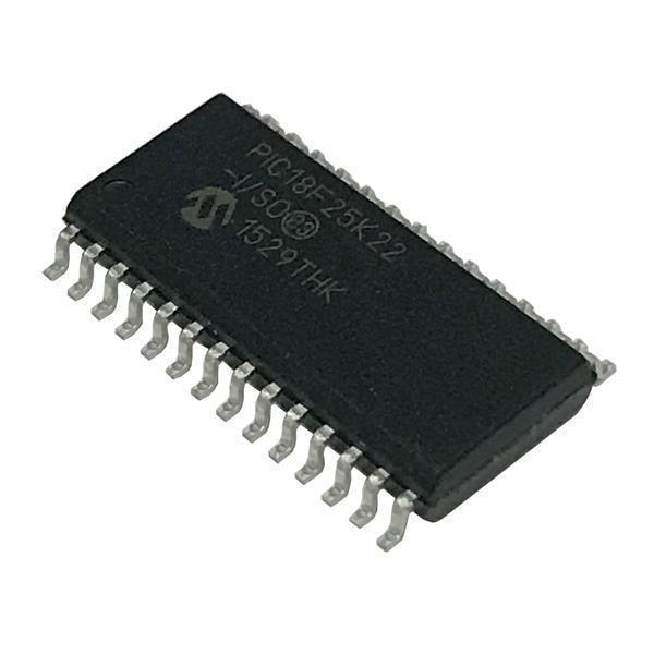
Restoring Microcontroller PIC18F25K22 Memory Heximal
Restoring Microcontroller PIC18F25K22 Memory Heximal from flash after crack mcu pic18f25k22 fuse bit and read embedded firmware from processor.

The Internal Oscillator Frequency Select bits (IRCF<2:0>) select the frequency output of the internal oscillator block. The choices are the LFINTOSC source (31.25 kHz), the MFINTOSC source (31.25 kHz, 250 kHz or 500 kHz) and the HFINTOSC source (16 MHz) or one of the frequencies derived from the HFINTOSC postscaler (31.25 kHz to 8 MHz).
ripristino del microcontrollore protetto PIC18F25K22 del codice esagonale della memoria flash e del file di dati della memoria EEPROM dopo che l’MCU crittografato PIC18F25K22 il pezzo del fusibile di sicurezza dell’MCU ed estrasse il firmware incorporato dal PIC18F25K22 bloccato del microprocessore.
If the internal oscillator block is supplying the main clock, changing the states of these bits will have an immediate change on the internal oscillator’s output to faciliate the process of recovering pic18f24k22 flash memory. On device Resets, the output frequency of the internal oscillator is set to the default frequency of 1 MHz.
When a nominal output frequency of 31.25 kHz is selected (IRCF<2:0> = 000), users may choose which internal oscillator acts as the source. This is done with the INTSRC bit of the OSCTUNE register and MFIOSEL bit of the OSCCON2 register. See Figure 2-2 and Register 2-1 for specific 31.25 kHz selection.
Przywracanie zabezpieczonego kodu szesnastkowego pamięci flash PIC18F25K22 mikrokontrolera i pliku danych pamięci EEPROM po złamaniu zaszyfrowanego MCU PIC18F25K22 bitu bezpiecznika bezpieczeństwa i wyodrębnieniu wbudowanego oprogramowania układowego z zablokowanego PIC18F25K22 mikroprocesora.
This option allows users to select a 31.25 kHz clock (MFINTOSC or HFINTOSC) that can be tuned using the TUN<5:0> bits in OSCTUNE register, while maintaining power savings with a very low clock speed. LFINTOSC always remains the clock source for features such as the Watchdog Timer and the Fail-Safe Clock Monitor, regardless of the setting of INTSRC and MFIOSEL bits This option allows users to select the tunable and more precise HFINTOSC as a clock source when break microchip pic18f25k80 loaded memory, while maintaining power savings with a very low clock speed.
استعادة متحكم آمن PIC18F25K22 ذاكرة فلاش رمز سداسي وملف بيانات ذاكرة EEPROM بعد الكراك المشفر MCU PIC18F25K22 بت الصمامات الأمنية واستخراج البرامج الثابتة المضمنة من PIC18F25K22 المعالجات الدقيقة المقفلة.
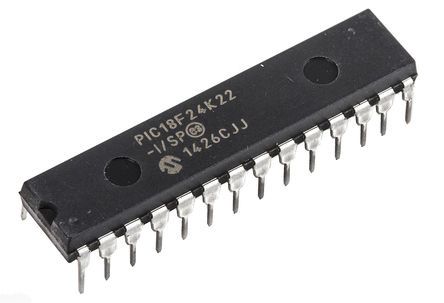
Microchip PIC18F24K22 Locked Flash Memory Code Recovery
Microchip PIC18F24K22 Locked Flash Memory Code Recovery needs to crack mcu pic18f24k22 protective system and read the embedded heximal out from microcontroller flash memory;
Besides its availability as a clock source, the internal oscillator block provides a stable reference source that gives the family additional features for robust operation:
- Fail-Safe Clock Monitor: This option constantly monitors the main clock source against a reference signal provided by the LFINTOSC. If a clock failure occurs, the controller is switched to the internal oscillator block, allowing for continued operation or a safe application shutdown.

Microchip PIC18F24K22 il recupero del codice della memoria flash bloccata deve decodificare il sistema di protezione PIC18F24K22 MCU protetto e leggere il firmware incorporato dei dati esamidali o del programma binario dal microcontrollore PIC18F24K22 dalla memoria flash e dalla memoria eeprom;
Two-Speed Start-up: This option allows the internal oscillator to serve as the clock source from Power-on Reset, or wake-up from Sleep mode, until the primary clock source is available.
- Memory Endurance: The Flash cells for both program memory and data EEPROM are rated to last for many thousands of erase/write cycles – up to 10K for program memory and 100K for EEPROM attacked by brutel force. Data retention without refresh is conservatively estimated to be greater than 40 years.
- Self-programmability: These devices can write to their own program memory spaces under inter- nal software control. By using a bootloader routine located in the protected Boot Block at the top of program memory, it becomes possible to create an application that can update itself in the field.
Odzyskiwanie kodu zablokowanej pamięci flash PIC18F24K22 mikroprocesora wymaga dekodowania zabezpieczonego systemu ochronnego MCU PIC18F24K22 i odczytu wbudowanego oprogramowania układowego danych szesnastkowych lub programu binarnego z mikrokontrolera PIC18F24K22 pamięci flash i pamięci EEPROM;
- Extended Instruction Set: The PIC18(L)F2X/ 4XK22 family introduces an optional extension to the PIC18 instruction set, which adds 8 new instructions and an Indexed Addressing mode. This extension, enabled as a device configuration option, has been specifically designed to optimize re-entrant application code originally developed in high-level languages, such as C.
- Enhanced CCP module: In PWM mode, this module provides 1, 2 or 4 modulated outputs for controlling half-bridge and full-bridge drivers. Other features include:
- Auto-Shutdown, for disabling PWM outputs on interrupt or other select conditions
- Auto-Restart, to reactivate outputs once the condition has cleared
رقاقة PIC18F24K22 استعادة رمز ذاكرة فلاش مقفلة يحتاج إلى فك تشفير MCU الآمن PIC18F24K22 نظام الحماية وقراءة البرامج الثابتة المضمنة للبيانات السداسية أو البرنامج الثنائي من متحكم PIC18F24K22 ذاكرة فلاش وذاكرة eeprom ؛
Output steering to selectively enable one or more of 4 outputs to provide the PWM signal
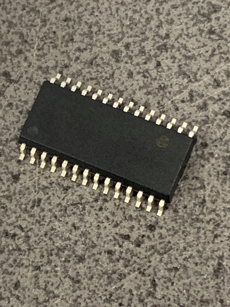
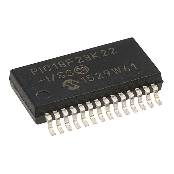
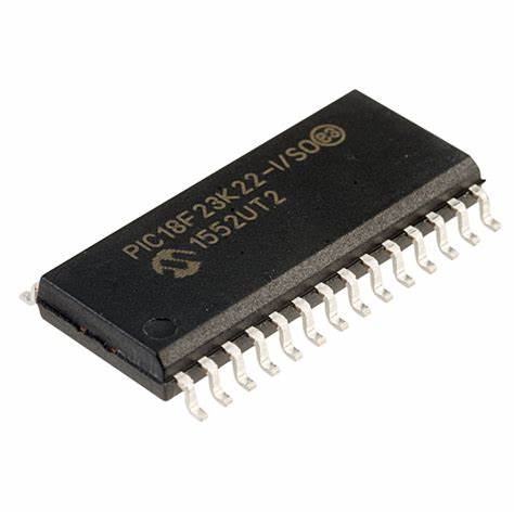
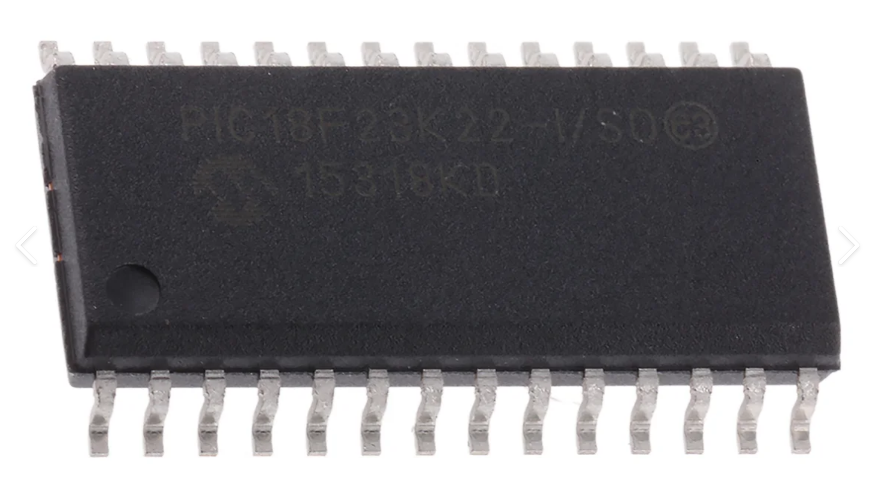
Break Microchip Microcontroller PIC18F23K22 Flash
Break Microchip Microcontroller PIC18F23K22 Flash needs to crack mcu pic18f23k22 fuse bit and readout the firmware from embedded mcu which will provide the same functions as original heximal;
All of the devices in the PIC18(L)F2X/4XK22 family incorporate a range of features that can significantly reduce power consumption during operation. Key items include:
Alternate Run Modes: By clocking the controller from the Timer1 source or the internal oscillator block, power consumption during mcu code execution can be reduced by as much as 90%.
rompere il microcontrollore protettivo Microchip PIC18F23K22 memoria flash deve decrittografare il bit di fusibile PIC18F23K22 MCU protetto ed estrarre il microprocessore bloccato PIC18F23K22 il firmware incorporato dalla memoria flash e eeprom che fornirà le stesse funzioni dei dati esatali originali o del codice sorgente binario;
Multiple Idle Modes: The controller can also run with its CPU core disabled but the peripherals still active. In these states, power consumption can be reduced even further, to as little as 4% of normal operation requirements.
On-the-fly Mode Switching: The power- managed modes are invoked by user code during operation, allowing the user to incorporate power- saving ideas into their application’s software design.
przerwać mikrokontroler ochronny Microchip PIC18F23K22 pamięć flash musi odszyfrować zabezpieczony mikroprocesor PIC18F23K22 bit bezpiecznika i wyodrębnić zablokowany mikroprocesor PIC18F23K22 wbudowane oprogramowanie układowe z pamięci flash i eeprom, które zapewnią te same funkcje, co oryginalne dane szesnastkowe lub binarny kod źródłowy;
Low Consumption in Key Modules: The power requirements for both Timer1 and the Watchdog Timer are minimized. See Section 27.0 “Electrical Characteristics” for values.
All of the devices in the PIC18(L)F2X/4XK22 family offer ten different oscillator options, allowing users a wide range of choices in developing application hardware. These include:
كسر متحكم دقيق واقية رقاقة PIC18F23K22 ذاكرة فلاش يحتاج إلى فك تشفير MCU الآمن PIC18F23K22 بت الصمامات واستخراج المعالجات الدقيقة المقفلة PIC18F23K22 البرامج الثابتة المضمنة من ذاكرة الفلاش وذاكرة eeprom والتي ستوفر نفس وظائف البيانات السداسية الأصلية أو شفرة المصدر الثنائية ؛
- Four Crystal modes, using crystals or ceramic resonators
- Two External Clock modes, offering the option of using two pins (oscillator input and a divide-by-4 clock output) or one pin (oscillator input, with the second pin reassigned as general I/O)
Two External RC Oscillator modes with the same pin options as the External Clock modes
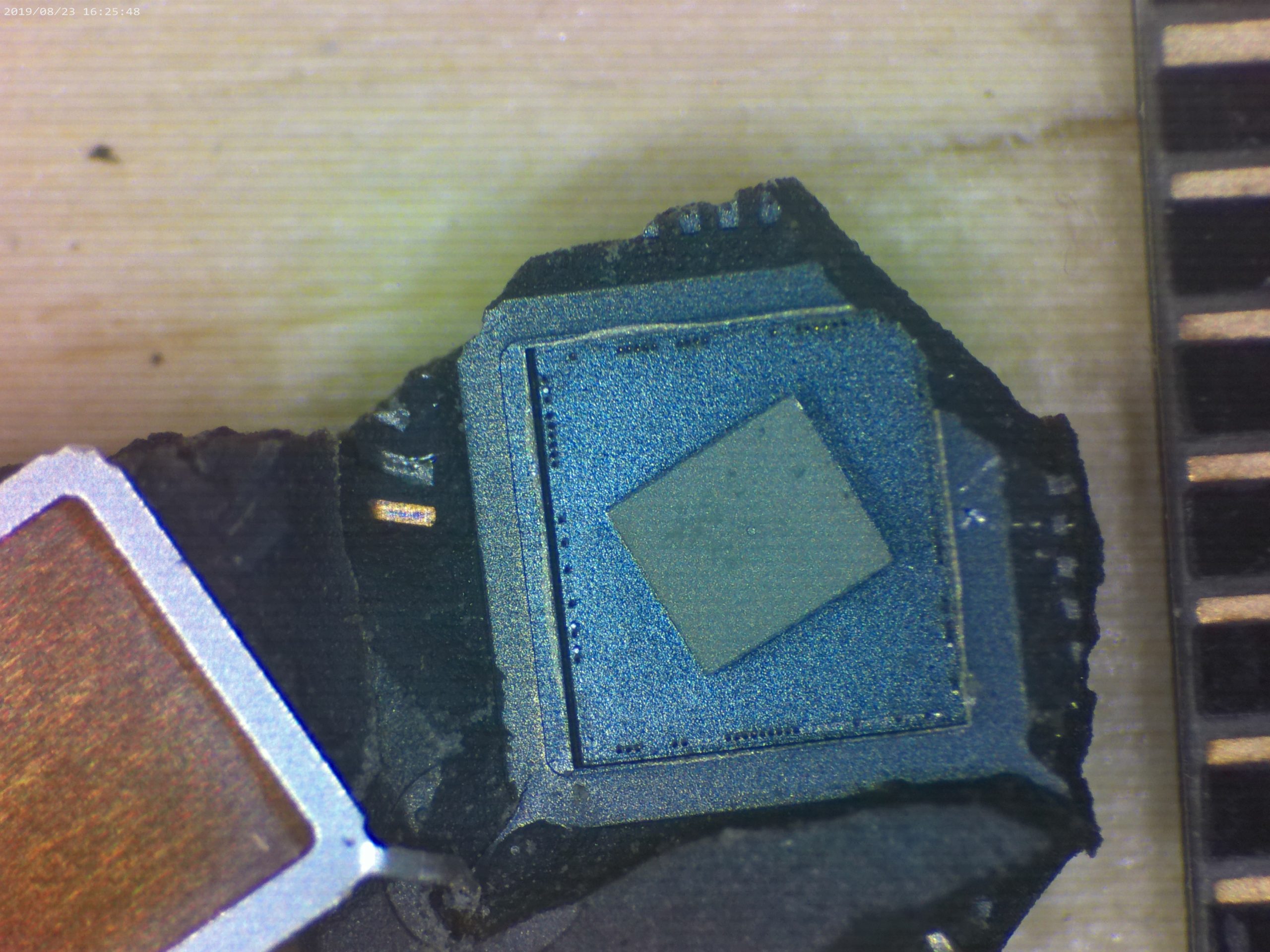
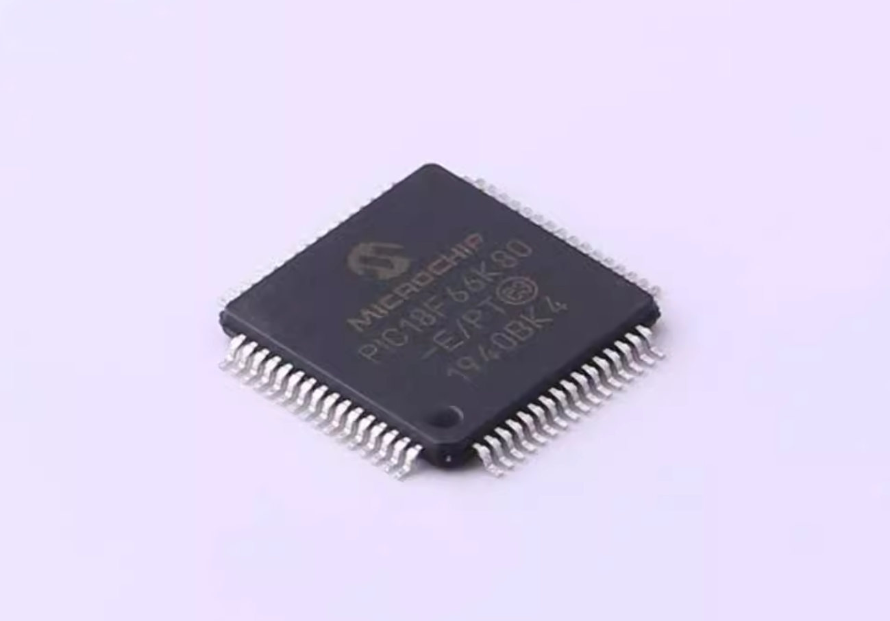
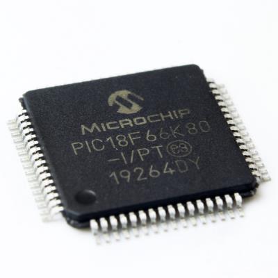
Restoring PIC18F66K80 MCU Controller Embedded Heximal
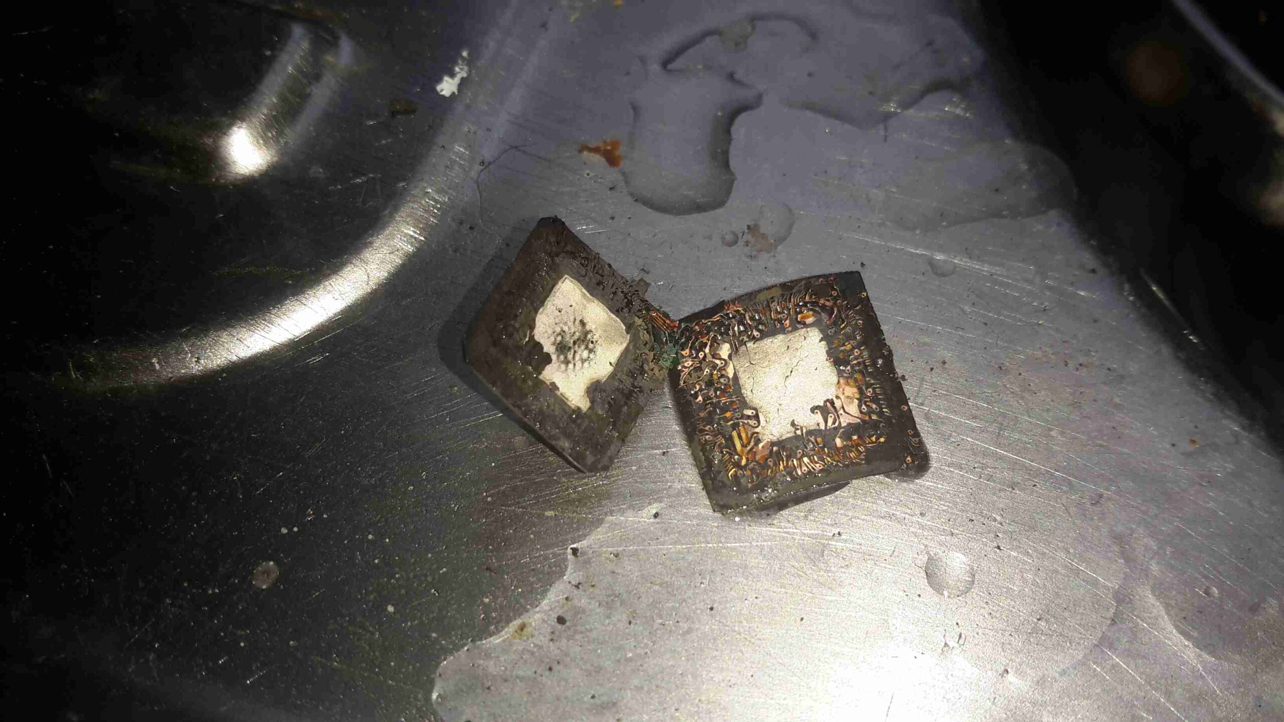
Restoring PIC18F66K80 MCU Controller Embedded Heximal from encrypted flash and eeprom memory, unlock security fuse bit of mcu pic18f66k80 by focus ion beam and extract mcu code;
Using the internal oscillator as the clock source elimi- nates the need for up to two external oscillator pins, which can then be used for digital I/O. Two distinct oscillator configurations, which are determined by the FOSCx Configuration bits, are available:
restaurar PIC18F66K80 firmware embutido microprocessador bloqueado, incluindo dados heximais da memória flash criptografada e arquivo binário da memória eeprom, desbloquear bit de fusível de segurança do MCU PIC18F66K80 por feixe de íons de foco e extrair microcontrolador protetor PIC18F66K80 código-fonte;
- In INTIO1 mode, the OSC2 pin (RA6) outputs FOSC/4, while OSC1 functions as RA7 for digital input and output.
In INTIO2 mode, OSC1 functions as RA7 and OSC2 functions as RA6. Both are available as digital input and output ports.
The 4x Phase Lock Loop (PLL) can be used with the HF-INTOSC to produce faster device clock speeds than are normally possible with the internal oscillator sources to ensure the success . When enabled, the PLL produces a clock speed of 16 MHz or 64 MHz.
بازگرداندن PIC18F66K80 سیستم عامل جاسازی شده ریز پردازنده قفل شده از جمله داده های هگزیمال از حافظه فلش رمزگذاری شده و فایل باینری از حافظه eeprom، باز کردن فیوز امنیتی بیت از PIC18F66K80 MCU توسط پرتو یون تمرکز و استخراج میکروکنترلر محافظ PIC18F66K80 کد منبع؛
PLL operation is controlled through software. The control bits, PLLEN (OSCTUNE<6>) and PLLCFG (CONFIG1H<4>), are used to enable or disable its operation. The PLL is available only to HF-INTOSC. The other oscillator is set with HS and EC modes. Additionally, the PLL will only function when the selected output frequency is either 4 MHz or 16 MHz (OSCCON<6:4> = 111, 110 or 101) when duplicating pic18f26k20 source code.
Like the INTIO modes, there are two distinct INTPLL modes available:
восстановление PIC18F66K80 заблокированной встроенной прошивки микропроцессора, включая шестнадцатеричные данные из зашифрованной флэш-памяти и двоичный файл из памяти EEPROM, разблокировка бита предохранителя MCU PIC18F66K80 фокусировочным ионным пучком и извлечение защитного микроконтроллера PIC18F66K80 исходный код;
- In INTPLL1 mode, the OSC2 pin outputs FOSC/4, while OSC1 functions as RA7 for digital input and output. Externally, this is identical in appearance to INTIO1.
In INTPLL2 mode, OSC1 functions as RA7 and OSC2 functions as RA6, both for digital input and output. Externally, this is identical to INTIO2.
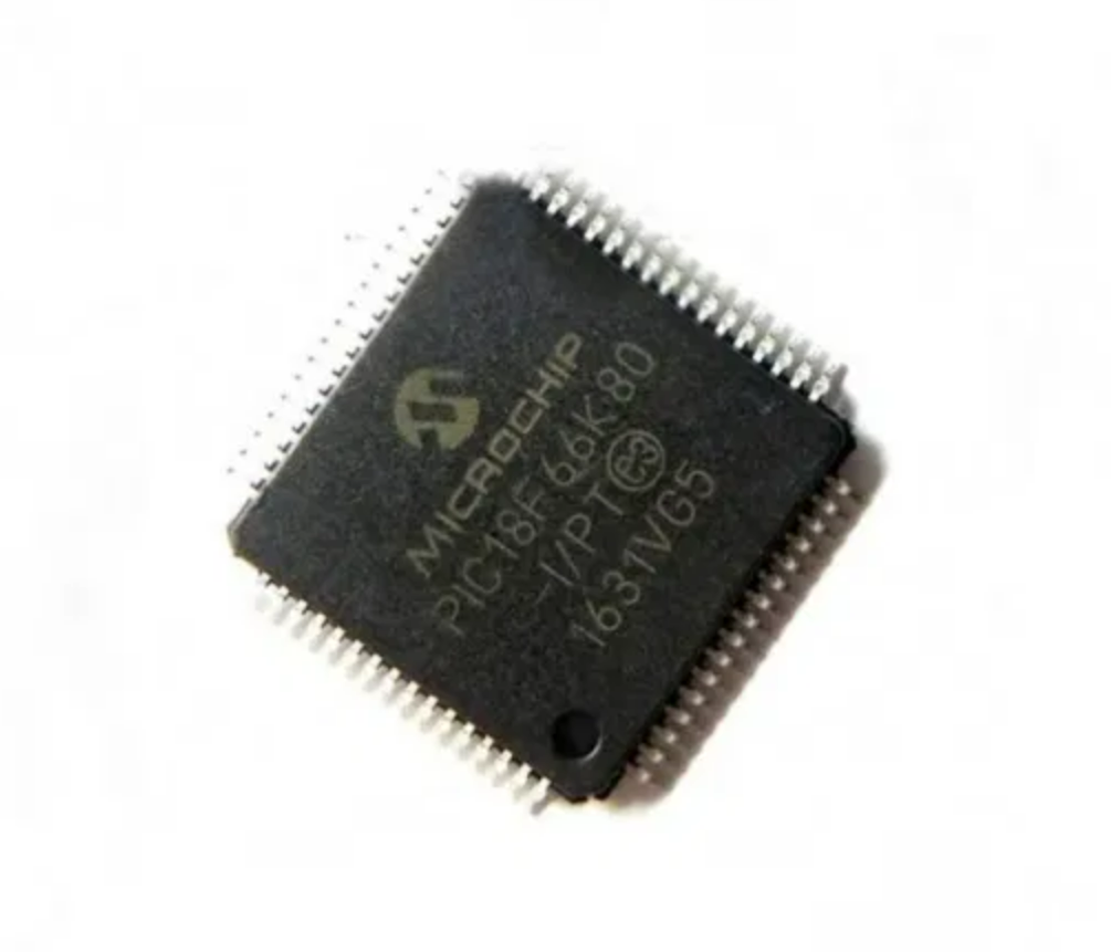
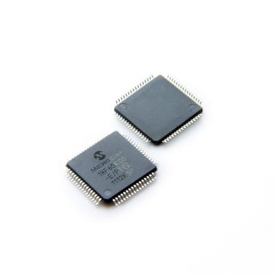
Microchip MCU PIC18F65K80 Heximal Recovery
Microchip MCU PIC18F65K80 Heximal Recovery is a process to unlock microcontroller pic18f65k80 secured memory and then readout the embedded firmware from mcu;
The PIC18F66K80 family of devices includes an internal oscillator block which generates two different clock signals. Either clock can be used as the microcontroller’s clock source, which may eliminate the need for an external oscillator circuit on the OSC1 and/or OSC2 pins.
The Internal oscillator consists of three blocks, depending on the frequency of operation. They are HF-INTOSC, MF-INTOSC and LF-INTOSC.
Microchip MCU PIC18F65K80 dados binários ou recuperação de programa heximal é um processo para desbloquear microcontrolador seguro PIC18F65K80 memória flash e memória eeprom fusível protetor bit, ler firmware incorporado, como o código-fonte do microprocessador criptografado PIC18F65K80;
In HF-INTOSC mode, the internal oscillator can provide a frequency ranging from 31 KHz to 16 MHz, with the postscaler deciding the selected frequency (IRCF<2:0>).
The INTSRC bit (OSCTUNE<7>) and MFIOSEL bit
(OSCCON2<0>) also decide which INTOSC provides the lower frequency (500 kHz to 31 KHz). For the HF-INTOSC to provide these frequencies, INTSRC = 1 and MFIOSEL = 0.
Микроконтроллер микросхемы PIC18F65K80 двоичных данных или восстановления шестнадцатеричной программы – это процесс разблокировки защищенного микроконтроллера PIC18F65K80 флэш-памяти и защитного бита памяти EEPROM, считывания встроенной прошивки, такой как исходный код зашифрованного микропроцессора PIC18F65K80;
In HF-INTOSC, the postscaler (IRCF<2:0>) provides the frequency range of 31 kHz to 16 MHz. If HF-INTOSC is used with the PLL, the input frequency to the PLL should be 4 MHz to 16 MHz (IRCF<2:0> = 111, 110 or 101) by breaking microchip pic18f25k80 flash memory.
For MF-INTOSC mode to provide a frequency range of 500 kHz to 31 kHz, INTSRC = 1 and MFIOSEL = 1.
The postscaler (IRCF<2:0>), in this mode, provides the
frequency range of 31 kHz to 500 kHz.
The LF-INTOSC can provide only 31 kHz if INTSRC = 0.
میکروچیپ MCU PIC18F65K80 داده های باینری یا بازیابی برنامه هگزیمال یک فرایند برای باز کردن میکروکنترلر امن PIC18F65K80 حافظه فلش و حافظه eeprom محافظ فیوز بیت، بازخوانی سیستم عامل تعبیه شده مانند کد منبع از ریزپردازنده رمزگذاری شده PIC18F65K80 است؛
The LF-INTOSC provides 31 kHz and is enabled if it is selected as the device clock source. The mode is enabled automatically when any of the following are enabled:
- Power-up Timer (PWRT)
- Fail-Safe Clock Monitor (FSCM)
- Watchdog Timer (WDT)
- Two-Speed Start-up
These features are discussed in greater detail in
Section 28.0 “Special Features of the CPU”.
The clock source frequency (HF-INTOSC, MF-INTOSC or LF-INTOSC direct) is selected by configuring the IRCFx bits of the OSCCON register, as well the INTSRC and MFIOSEL bits. The default frequency on device Resets is 8 MHz.