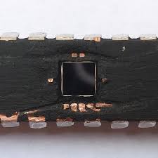
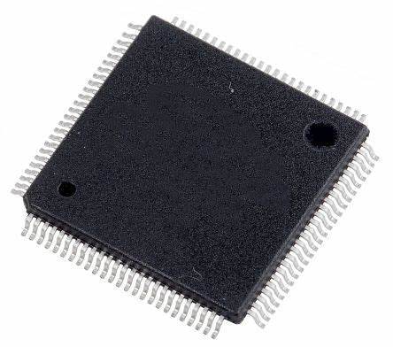
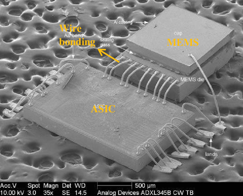
 Attack Renesas R5F51115ADFM#3A MCU Flash Memory
Attack Renesas R5F51115ADFM#3A MCU Flash Memory and extract embedded binary from microcontroller flash memory and download it to new MCU for cloning purpose;
During sleep mode or mode transitions, do not write to the system control related registers (indicated by ‘SYSTEM’ in the Module Symbol column in Table 4.1, List of I/O Registers (Address Order)).
Permanent damage to the MCU may result if absolute maximum ratings are exceeded.
To preclude any malfunctions due to noise interference, insert capacitors of high frequency characteristics between the VCC and VSS pins, between the AVCC0 and AVSS0 pins, between the VCC_USB and VSS_USB pins, and between the VREFH0 and VREFL0 pins.
атакувати флеш-пам’ять MCU Renesas R5F51115ADFM#3A і витягти вбудовану двійкову або шістнадцяткову програмну прошивку з флеш-пам’яті мікроконтролера R5F51115ADFM#3A і скопіювати її в новий MCU з метою клонування;
Place capacitors of about 0.1 μF as close as possible to every power supply pin and use the shortest and heaviest possible traces. Also, connect capacitors as stabilization capacitance which will help to facilitate the process of cracking renesas mcu r5f563nfddf flash memory.
Connect the VCL pin to a VSS pin via a 4.7 μF capacitor. The capacitor must be placed close to the pin, refer to section 5.12.1, Connecting VCL Capacitor and Bypass Capacitors.
Do not input signals or an I/O pull-up power supply to ports other than 5-V tolerant ports while the device is not powered. The current injection that results from input of such a signal or I/O pull-up may cause malfunction and the abnormal current that passes in the device at this time may cause degradation of internal elements.
Renesas R5F51115ADFM#3A MCU flash belleğe saldırın ve mikrodenetleyici R5F51115ADFM#3A flash bellekten gömülü ikili veya onaltılık program bellenimini çıkarın ve klonlama amacıyla yeni MCU’ya kopyalayın;
If input voltage (within the specified range from -0.3 to + 6.5V) is applied to 5-V tolerant ports, it will not cause problems such as damage to the MCU.
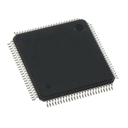
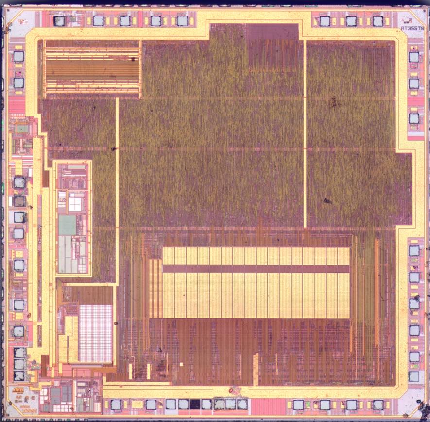
Crack Renesas Microcontroller R5F563NFDDFP#V0 Flash Memory
Crack Renesas Microcontroller R5F563NFDDFP#V0 Flash Memory and break MCU tamper resistance system, readout locked firmware from secured microprocessor and copy the binary to new MCU;
The number of bus cycles of internal peripheral buses 1 to 6 differs according to the register to be accessed.
When peripheral functions connected to internal peripheral buses 2 to 6 or registers for the external bus control unit (except for bus error related registers) are accessed, the number of divided clock synchronization cycles is added.
The number of divided clock synchronization cycles differs depending on the frequency ratio between ICLK and PCLK (or FCLK) or bus access timing.
зламати мікроконтролер Renesas R5F563NFDDFP#V0 флеш-пам’ять і зламати MCU R5F563NFDDFP#V0 систему стійкості до несанкціонованого доступу, зчитування заблокованої прошивки в форматі двійкового або шістнадцяткового з захищеного мікропроцесора і скопіювати вихідний код прошивки в новий MCU R5F563NFDDFP#V0;
In the peripheral function unit, when the frequency ratio of ICLK is equal to or greater than that of PCLK (or FCLK), the sum of the number of bus cycles for internal main bus 1 and the number of the divided clock synchronization cycles will be one cycle of PCLK (or FCLK) at a maximum.
Therefore, one PCLK (or FCLK) has been added to the number of access cycles shown in Table 4.1.
When the frequency ratio of ICLK is lower than that of PCLK (or FCLK), the subsequent bus access is started from the ICLK cycle following the completion of the access to the peripheral functions to crack renesas mcu R5F52108 Flash memory. Therefore, the access cycles are described on an ICLK basis.
Renesas mikrodenetleyici R5F563NFDDFP # V0 flash belleği kırın ve MCU R5F563NFDDFP # V0 kurcalama direnci sistemini kırın, güvenli mikroişlemciden ikili veya onaltılık biçiminde kilitli bellenimi okuyun ve bellenim kaynak kodunu yeni MCU’ya kopyalayın R5F563NFDDFP # V0;
Note 1. This applies to the number of cycles when the access from the CPU does not conflict with the bus access from the different bus master (DTC).
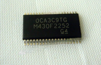
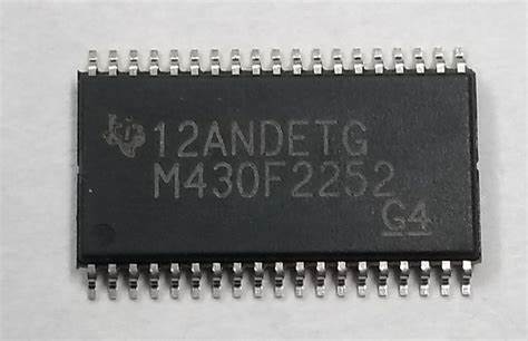
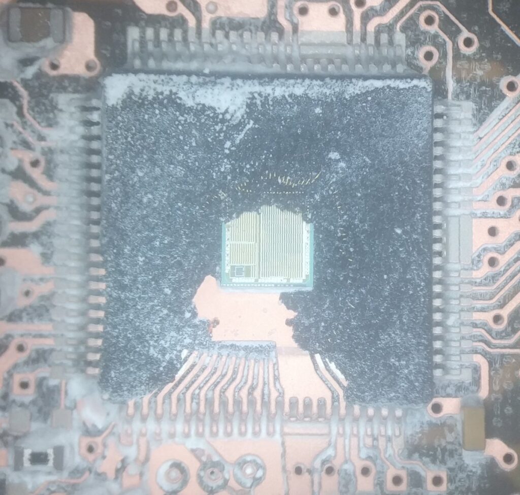
Attack Microprocessor MSP430F2252 Secured Flash
Attack Microprocessor MSP430F2252 Secured Flash memory and extract locked heximal code from msp430g2252 mcu, to make new microcontroller cloning units;
The Texas Instruments MSP430™ family of ultra-low-power microcontrollers consist of several devices featuring different sets of peripherals targeted for various applications.
The architecture, combined with five low-power modes, is optimized to achieve extended battery life in portable measurement applications. The device features a powerful 16-bit RISC CPU, 16-bit registers, and constant generators that contribute to maximum code efficiency when restoring flash memory content of microcontroller msp430g2452.
güvenli flash bellek koruma sistemi MSP430F2252 mikroişlemciye saldırmak ve MSP430F2252 mikrodenetleyiciden kilitli onaltılık program veya ikili kaynak kodunu çıkarmak, yeni MCU MSP430F2252 çip klonlanmış birimleri boşaltmak için bellenimi kopyalamak;
The digitally controlled oscillator (DCO) allows wake-up from low-power modes to active mode in less than 1 µs.
The MSP430G2x52 and MSP430G2x12 series of microcontrollers are ultra-low-power mixed signal microcontrollers with built-in 16-bit timers, and up to 16 I/O touch sense enabled pins and built-in communication capability using the universal serial communication interface and have a versatile analog comparator which are critical point for texas instrument microcontroller flash program extraction.
атакувати мікропроцесор MSP430F2252 захищену систему флеш-пам’яті та витягти заблоковану шістнадцяткову програму або двійковий вихідний код з MSP430F2252 мікроконтролера, скопіювати прошивку для скидання нових блоків MCU MSP430F2252 клонованих мікросхем;
The MSP430G2x52 series have a 10-bit A/D converter. For configuration details see Table 1. Typical applications include low-cost sensor systems that capture analog signals, convert them to digital values, and then process the data for display or for transmission to a host system.
Break TI MSP430G2452 Microcontroller Flash Memory
Break TI MSP430G2452 Microcontroller Flash Memory and extract embedded firmware from msp430g2452 flash memory, after break mcu msp430g2452 protective system;
The MSP430 CPU has a 16-bit RISC architecture that is highly transparent to the application. All operations, other than program-flow instructions, are performed as register operations in conjunction with seven addressing modes for source operand and four addressing modes for destination operand to attack microcontroller msp430g2452 flash memory.
złamać bezpiecznik ochronny pamięci flash mikrokontrolera TEXAS INSTRUMENT MSP430G2452 i wyodrębnić wbudowane oprogramowanie sprzętowe z pamięci flash MSP430G2452 w formacie binarnym lub szesnastkowym, skopiuj kod źródłowy MCU MSP430G2452 do nowego chipa, aby sklonować oryginalny mikrokomputer;
The CPU is integrated with 16 registers that provide reduced instruction execution time. The register-to-register operation execution time is one cycle of the CPU clock.
TEXAS INSTRUMENT MSP430G2452 mikrodenetleyici flash bellek koruyucu sigorta bitini kırın ve MSP430G2452 flash bellekten ikili veya onaltılı formatta gömülü bellenimi çıkarın, orijinal mikro bilgisayarı klonlamak için MCU MSP430G2452 kaynak kodunu yeni çipe kopyalayın;
Four of the registers, R0 to R3, are dedicated as program counter, stack pointer, status register, and constant generator, respectively. The remaining registers are general-purpose registers. Peripherals are connected to the CPU using data, address, and control buses, and can be handled with all instructions in order to facilitate the process of recovering microcontroller 430g2452 flash memory.
Texas Instrument MSP430F2352 Microprocessor Breaking
Texas Instrument MSP430F2352 Microprocessor Breaking is a process to hack the tamper resistance system of texas instrument microcontroller chip flash memory and then readout the flash program from MCU msp430f2352;
The Texas Instruments MSP430™ family of ultra-low-power microcontrollers consist of several devices featuring different sets of peripherals targeted for various applications.
The architecture, combined with five low-power modes, is optimized to achieve extended battery life in portable measurement applications. The device features a powerful 16-bit RISC CPU, 16-bit registers, and constant generators that contribute to maximum code efficiency.
Deszyfrowanie zabezpieczonego mikroprocesora TEXAS INSTRUMENT MSP430F2352 to proces polegający na złamaniu systemu zabezpieczenia przed manipulacją zablokowanej pamięci flash chipa MSP430F2352, a następnie odczytaniu programu flash w formacie binarnym lub szesnastkowym z MCU MSP430F2352;
The digitally controlled oscillator (DCO) allows wake-up from low-power modes to active mode in less than 1 µs.
The MSP430G2x52 and MSP430G2x12 series of microcontrollers are ultra-low-power mixed signal microcontrollers with built-in 16-bit timers, and up to 16 I/O touch sense enabled pins and built-in communication capability using the universal serial communication interface and have a versatile analog comparator which are critical point for texas instrument microcontroller flash program extraction.
TEXAS INSTRUMENT MSP430F2352 güvenli mikroişlemci şifre çözme, kilitli mikrodenetleyici MSP430F2352 çip flash belleğinin kurcalamaya karşı koruma sistemini kırmak ve ardından MCU MSP430F2352’den ikili veya onaltılık formattaki flash programını okumak için bir işlemdir;
The MSP430G2x52 series have a 10-bit A/D converter. For configuration details see Table 1. Typical applications include low-cost sensor systems that capture analog signals, convert them to digital values, and then process the data for display or for transmission to a host system when attacking mcu msp430g2452 secured system.
Restoring Mixed Signal MSP430G2452 CPU Flash Binary
Restoring Mixed Signal MSP430G2452 CPU Flash Binary from its locked memory after break mcu msp430g2452 protective system and extract the embedded firmware from microcontroller msp430g2452 memory;

The Texas Instruments MSP430™ family of ultra-low-power microcontrollers consist of several devices featuring different sets of peripherals targeted for various applications. The architecture, combined with five low-power modes, is optimized to achieve extended battery life in portable measurement applications.
karışık sinyal MSP430G2452 şifrelenmiş mikroişlemci flash program dosyasının ikili veya onaltılı formatta kilitli MCU’nun belleğinden kilitli mikroişlemci MSP430G2452 koruyucu sisteminin geri yüklenmesi ve gömülü aygıt yazılımının güvenli mikro bilgisayar MSP430G2452 belleğinden çıkarılması;
The device features a powerful 16-bit RISC CPU, 16-bit registers, and constant generators that contribute to maximum code efficiency. The digitally controlled oscillator (DCO) allows wake-up from low-power modes to active mode in less than 1 µs.
The MSP430G2x52 and MSP430G2x12 series of microcontrollers are ultra-low-power mixed signal microcontrollers with built-in 16-bit timers, and up to 16 I/O touch sense enabled pins and built-in communication capability using the universal serial communication interface and have a versatile analog comparator to recover the program from msp430g2452.
przywracanie sygnału mieszanego MSP430G2452 zaszyfrowanego pliku programu flash oprogramowania sprzętowego w formacie binarnym lub szesnastkowym z zablokowanej pamięci MCU po uszkodzeniu zablokowanego systemu zabezpieczającego mikroprocesora MSP430G2452 i wyodrębnienie wbudowanego oprogramowania sprzętowego z zabezpieczonej pamięci mikrokomputera MSP430G2452;
The MSP430G2x52 series have a 10-bit A/D converter. For configuration details see Table 1. Typical applications include low-cost sensor systems that capture analog signals, convert them to digital values, and then process the data for display or for transmission to a host system.
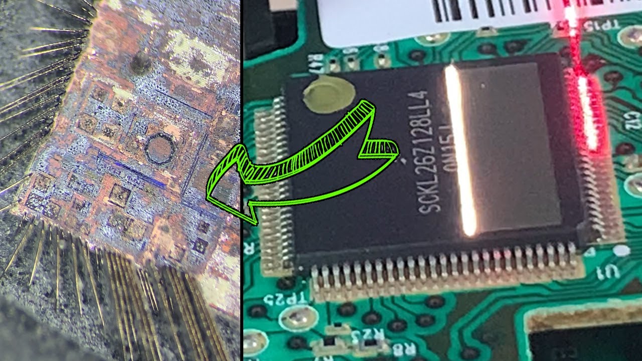
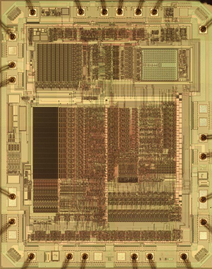
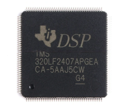
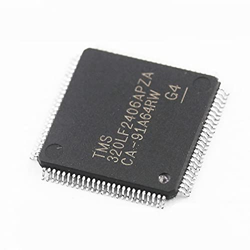
Duplicating DSP Microprocessor TMS320LF2407 Flash Program
Duplicating DSP Microprocessor TMS320LF2407 Flash Program to new MCU TMS320LF2407, the embedded firmware will be decrypted by MCU TMS320LF2407 flash and make new microcontroller copies;
Output clock derived from SYSCLKOUT. XCLKOUT is either the same frequency, one-half the frequency, or one-fourth the frequency of SYSCLKOUT. This is controlled by bits 1:0 (XCLKOUTDIV) in the XCLK register.
At reset, XCLKOUT = SYSCLKOUT/4. The XCLKOUT signal can be turned off by setting XCLKOUTDIV to 3. The mux control for GPIO18 must also be set to XCLKOUT for this signal to propogate to the pin.
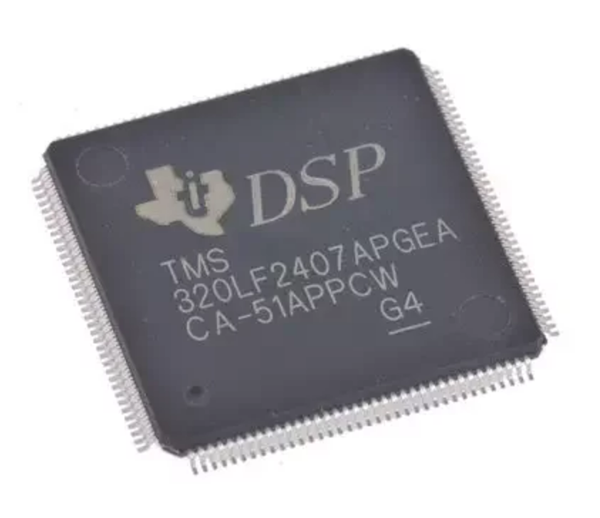
дублировать программу флэш-памяти микропроцессора TMS320LF2407 с защитой DSP на новый MCU TMS320LF2407, встроенная прошивка в двоичном или шестнадцатеричном виде будет расшифрована флэш-памятью MCU TMS320LF2407 и создаст новые копии микроконтроллера;
See GPIO19 and GPIO38. External oscillator input. Pin source for the clock is controlled by the XCLKINSEL bit in the XCLK register, GPIO38 is the default selection. This pin feeds a clock from an external 3.3-V oscillator. In this case, the X1 pin, if available, must be tied to GND and the on-chip crystal oscillator must be disabled through bit 14 in the CLKCTL register WHEN replicating dsp tms320lf2406 flash memory data.
Duplizieren Sie das Flash-Speicherprogramm des DSP-geschützten Mikroprozessors TMS320LF2407 auf die neue MCU TMS320LF2407. Die eingebettete binäre oder hexadezimale Firmware wird vom MCU TMS320LF2407-Flash entschlüsselt und erstellt neue Kopien des Mikrocontrollers.
If a crystal or resonator is used, the XCLKIN path must be disabled by bit 13 in the CLKCTL register.NOTE: Designs that use the GPIO38/XCLKIN/TCK pin to supply an external clock for normal device operation may need to incorporate some hooks to disable this path during debug using the JTAG connector. This is to prevent contention with the TCK signal, which is active during JTAG debug sessions. The zero-pin internal oscillators may be used during this time to clock the device.
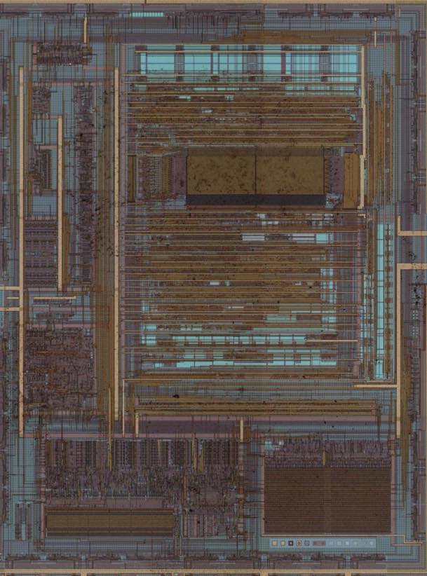
Replicating TI DSP Microcontroller TMS320LF2406 Memory Data
Replicating TI DSP Microcontroller TMS320LF2406 Memory Data and copy firmware to new MCU which will provide the same functions after reading mcu tms320lf2406 dsp chip flash code;
Below Table describes the signals. With the exception of the JTAG pins, the GPIO function is the default at reset, unless otherwise mentioned. The peripheral signals that are listed under them are alternate functions. Some peripheral functions may not be available in all devices.
репликация данных флэш-памяти микроконтроллера TMS320LF2406, зашифрованных TEXAS INSTRUMENT DSP, в двоичном или шестнадцатеричном виде, взлом заблокированной защитной системы микропроцессора или плавкого бита, копирование прошивки в новый MCU, который будет обеспечивать те же функции после считывания защищенного исходного кода микрокомпьютера TMS320LF2406;
See below Table for details. Inputs are not 5-V tolerant. All GPIO pins are I/O/Z and have an internal pullup (PU), which can be selectively enabled or disabled on a per-pin basis. This feature only applies to the GPIO pins to facilitate the process of duplicating dsp mcu tms320lf2407 memory program. The pullups on the PWM pins are not enabled at reset. The pullups on other GPIO pins are enabled upon reset. The AIO pins do not have an internal pullup;

Replizieren von TEXAS INSTRUMENT DSP-verschlüsselten Flash-Speicherdaten des Mikrocontrollers TMS320LF2406 als Binär- oder Heximaldaten, Aufbrechen des gesperrten Schutzsystems oder Sicherungsbits des Mikroprozessors, Kopieren der Firmware auf neue MCU, die nach dem Auslesen des gesicherten Quellcodes des Mikrocomputers TMS320LF2406 die gleichen Funktionen bereitstellt;
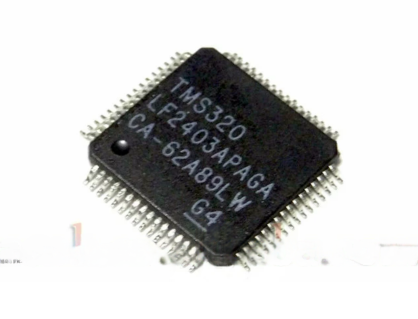
Restore DSP TMS320LF2403 Microprocessor Memory Program
Restore DSP TMS320LF2403 Microprocessor Memory Program starts from unlocking tms320f240 cpu flash memory and copy embedded firmware to new microcontroller;
C2000™ 32-bit microcontrollers are optimized for processing, sensing, and actuation to improve closed- loop performance in real-time control applications such as industrial motor drives; solar inverters and digital power; electrical vehicles and transportation; motor control; and sensing and signal processing. The C2000 line includes the Premium performance MCUs and the Entry performance MCUs.
The F2806x family of microcontrollers (MCUs) provides the power of the C28x core and CLA coupled with highly integrated control peripherals in low pin-count devices. This family is code-compatible with previous C28x-based code, and also provides a high level of analog integration.

восстановление заблокированной флэш-памяти микропроцессора DSP TMS320LF2403 начинается с взлома защищенного TMS320LF2403 защищенного плавкого предохранителя микрокомпьютера и системы защиты от несанкционированного доступа, а затем копируется встроенная прошивка в двоичном или шестнадцатеричном формате в новый микроконтроллер;
An internal voltage regulator allows for single-rail operation. Enhancements have been made to the HRPWM module to allow for dual-edge control (frequency modulation). Analog comparators with internal 10-bit references have been added and can be routed directly to control the ePWM outputs when restoring tms320f28067 dsp mcu locked flash program.
The ADC converts from 0 to 3.3-V fixed full-scale range and supports ratio-metric VREFHI/VREFLO references. The ADC interface has been optimized for low overhead and latency.
Wiederherstellen des gesperrten DSP TMS320LF2403-Mikroprozessor-Flash-Speicherprogramms beginnt mit dem durch einen Riss gesicherten TMS320LF2403-gesicherten Mikrocomputer-Sicherungsbit und Manipulationsschutzsystem und anschließendes Kopieren der eingebetteten Firmware im Binär- oder Heximalformat auf den neuen Mikrocontroller;
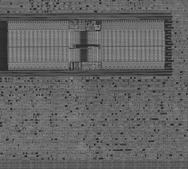
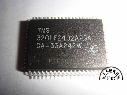
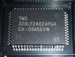
Break TI TMS320LF2402AP Microcontroller Flash Memory
Break TI TMS320LF2402AP Microcontroller Flash Memory and read out embedded firmware from MCU, copy tms320lf2402 flash memory program to new microprocessor for same cloning;
The devices are full static CMOS devices. Three low-power modes are provided:
IDLE:
Places CPU in low-power mode. Peripheral clocks may be turned off selectively and only those peripherals that must function during IDLE are left operating. An enabled interrupt from an active peripheral or the watchdog timer will wake the processor from IDLE mode.
STANDBY: Turns off clock to CPU and peripherals. This mode leaves the oscillator and PLL functional. An external interrupt event will wake the processor and the peripherals. Execution begins on the next valid cycle after detection of the interrupt event and then attack dsp mcu tms320f28232 flash memory;
كسر ذاكرة فلاش وحدة التحكم الدقيقة المقفلة TMS320LF2402AP والبرامج الثابتة المضمنة للقراءة الثنائية أو السداسية من MCU TMS320LF2402AP المشفرة، ونسخ برنامج ذاكرة فلاش TMS320LF2402AP إلى معالج دقيق مؤمن جديد لنفس الاستنساخ؛
HALT:
This mode basically shuts down the device and places it in the lowest possible power- consumption mode. If the internal zero-pin oscillators are used as the clock source, the HALT mode turns them off, by default. To keep these oscillators from shutting down, the INTOSCnHALTI bits in CLKCTL register may be used.
The zero-pin oscillators may thus be used to clock the CPU-watchdog in this mode. If the on-chip crystal oscillator is used as the clock source, it is shut down in this mode. A reset or an external signal (through a GPIO pin) or the CPU-watchdog can wake the device from this mode.
شکستن حافظه فلش میکروکنترلر قفل شده TMS320LF2402AP و بازخوانی سیستم عامل تعبیه شده باینری یا هگزیمال از MCU رمزگذاری شده TMS320LF2402AP، برنامه حافظه فلش TMS320LF2402AP را در ریزپردازنده ایمن جدید برای شبیه سازی مشابه کپی کنید.
The CPU clock (OSCCLK) and WDCLK should be from the same clock source before attempting to put the device into HALT or STANDBY.