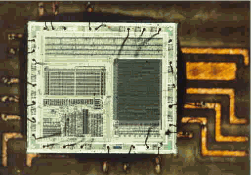
 Mixed Signal Microcontroller MSP430G2212 Flash Program Reverse Reading
Mixed Signal Microcontroller MSP430G2212 Flash Program Reverse Reading starts from cracking texas instrument msp430g2212 fuse bit, and readout embedded firmware from MSP430G2212 flash memory;
The MSP430 CPU has a 16-bit RISC architecture that is highly transparent to the application. All operations, other than program-flow instructions, are performed as register operations in conjunction with seven addressing modes for source operand and four addressing modes for destination operand.
The CPU is integrated with 16 registers that provide reduced instruction execution time. The register-to-register operation execution time is one cycle of the CPU clock when breaking texas instrument msp430g2352 microprocessor protection.
Four of the registers, R0 to R3, are dedicated as program counter, stack pointer, status register, and constant generator, respectively. The remaining registers are general-purpose registers.
Peripherals are connected to the CPU using data, address, and control buses, and can be handled with all instructions. The instruction set consists of the original 51 instructions with three formats and seven address modes and additional instructions for the expanded address range. Each instruction can operate on word and byte data.
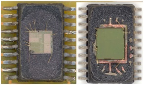
Reverse Texas Instrument MSP430G2112 Microcontroller Flash Memory
Reverse Texas Instrument MSP430G2112 Microcontroller Flash Memory is a process to unlock secured msp430g2112 mcu flash memory and then extract firmware program from msp430g2112 processor;
The Texas Instruments MSP430™ family of ultra-low-power microcontrollers consist of several devices featuring different sets of peripherals targeted for various applications. The architecture, combined with five low-power modes, is optimized to achieve extended battery life in portable measurement applications.
The device features a powerful 16-bit RISC CPU, 16-bit registers, and constant generators that contribute to maximum code efficiency. The digitally controlled oscillator (DCO) allows wake-up from low-power modes to active mode in less than 1 µs.
The MSP430G2x52 and MSP430G2x12 series of microcontrollers are ultra-low-power mixed signal microcontrollers with built-in 16-bit timers, and up to 16 I/O touch sense enabled pins and built-in communication capability using the universal serial communication interface and have a versatile analog comparator when restoring mixed signal mcu flash binary code.
The MSP430G2x52 series have a 10-bit A/D converter. For configuration details. Typical applications include low-cost sensor systems that capture analog signals, convert them to digital values, and then process the data for display or for transmission to a host system.
Break Mixed Signal MSP430G2211 Microcontroller Flash Memory
Break Mixed Signal MSP430G2211 Microcontroller Flash Memory and duplicate the embedded firmware from MSP430G2211 mcu memory in the format of heximal, copy firmware to new Microprocessor to perform the same functions:
Timer_A2 is a 16-bit timer/counter with two capture/compare registers. Timer_A2 can support multiple capture/compares, PWM outputs, and interval timing.
Timer_A2 also has extensive interrupt capabilities. Interrupts may be generated from the counter on overflow conditions and from each of the capture/compare registers.
The primary function of the comparator_A+module is to support precision slope analog-to-digital conversions, battery-voltage supervision, and monitoring of external analog signals which can be used for restoring microcontroller msp430g2101 flash content.
- Stresses beyond those listed under “absolute maximum ratings” may cause permanent damage to the device. These are stress ratings only, and functional operation of the device at these or any other conditions beyond those indicated under “recommended operating conditions” is not implied. Exposure to absolute-maximum-rated conditions for extended periods may affect device reliability.
- All voltages referenced to VSS. The JTAG fuse-blow voltage, VFB, is allowed to exceed the absolute maximum rating. The voltage is applied to the TEST pin when blowing the JTAG fuse.
- Higher temperature may be applied during board soldering according to the current JEDEC J-STD-020 specification with peak reflow temperatures not higher than classified on the device label on the shipping boxes or reels.
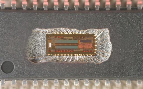
Attack Texas Instrument MSP430G2111 Microprocessor
Attack Texas Instrument MSP430G2111 Microprocessor and clone mcu msp430g2111 flash memory program from original MCU, copy binary firmware to new microcontroller;
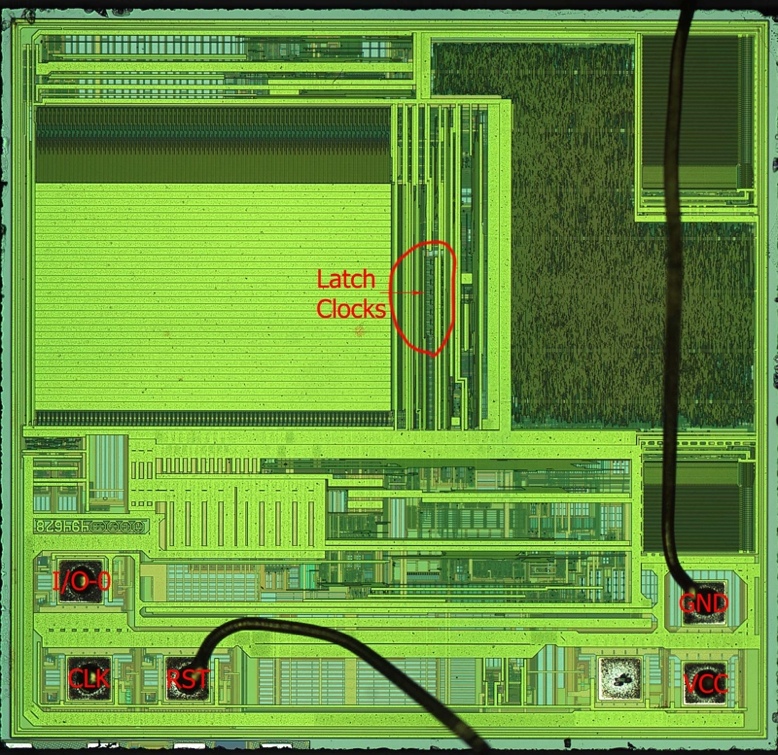
The flash memory can be programmed via the Spy-Bi-Wire/JTAG port or in-system by the CPU. The CPU can perform single-byte and single-word writes to the flash memory. Features of the flash memory include:
- Flash memory has n segments of main memory and four segments of information memory (A to D) of 64 bytes each. Each segment in main memory is 512 bytes in size.
- Segments 0 to n may be erased in one step, or each segment may be individually erased.
- Segments A to D can be erased individually or as a group with segments 0 to n. Segments A to D are also called information memory.
- Segment A contains calibration data. After reset segment A is protected against programming and erasing. It can be unlocked but care should be taken not to erase this segment if the device-specific calibration data is required.
Restore TI MCU MSP430G2101 Flash Content
Restore TI MCU MSP430G2101 Flash Content starts from unlock microcontroller msp430g2101 flash memory, its protective system will be removed and embedded firmware of flash memory of processor MSP430G2 will be readout;
The interrupt vectors and the power-up starting address are located in the address range 0FFFFh to 0FFC0h. The vector contains the 16-bit address of the appropriate interrupt handler instruction sequence. If the reset vector (located at address 0FFFEh) contains 0FFFFh (e.g., flash is not programmed) the CPU will go into LPM4 immediately after power-up which can be used for microcontroller mixed signal msp430g2452 memory binary file restoration.
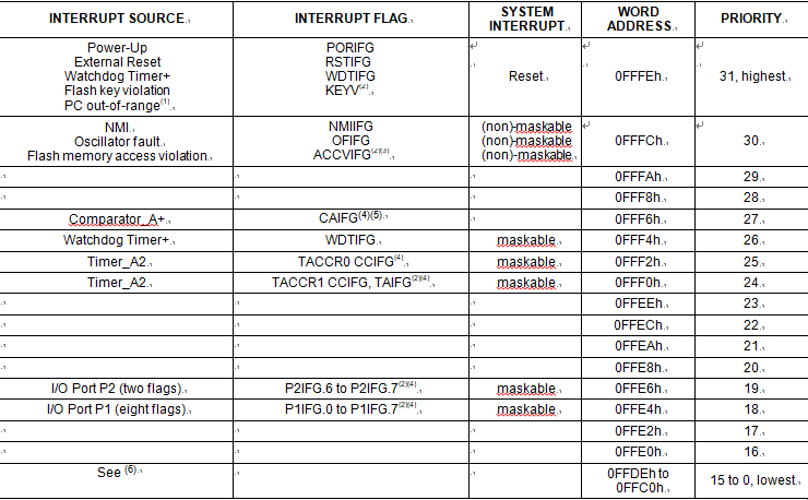
- A reset is generated if the CPU tries to fetch instructions from within the module register memory address range (0h to 01FFh) or from within unused address ranges.
- Multiple source flags
- (non)-maskable: the individual interrupt-enable bit can disable an interrupt event, but the general interrupt enable cannot.
- Interrupt flags are located in the module.
- Devices with Comparator_A+ only
- The interrupt vectors at addresses 0FFDEh to 0FFC0h are not used in this device and can be used for regular program code if necessary.
Restore Texas Instrument MSP430G2001 Microcontroller Heximal Program
Restore Texas Instrument MSP430G2001 Microcontroller Heximal Program from embedded flash memory after crack microcontroller msp430g2001 security fuse bit and extract IC code;
The MSP430 CPU has a 16-bit RISC architecture that is highly transparent to the application. All operations, other than program-flow instructions, are performed as register operations in conjunction with seven addressing modes for source operand and four addressing modes for destination operand.
The CPU is integrated with 16 registers that provide reduced instruction execution time. The register-to-register operation execution time is one cycle of the CPU clock.
Four of the registers, R0 to R3, are dedicated as program counter, stack pointer, status register, and constant generator, respectively. The remaining registers are general-purpose registers.
Peripherals are connected to the CPU using data, address, and control buses, and can be handled with all instructions. The instruction set consists of the original 51 instructions with three formats and seven address modes and additional instructions for the expanded address range. Each instruction can operate on word and byte data to increase the success rate of msp430g2452 microcontroller flash memory protection breaking.
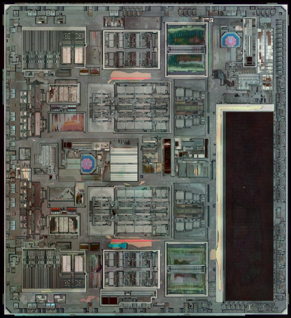
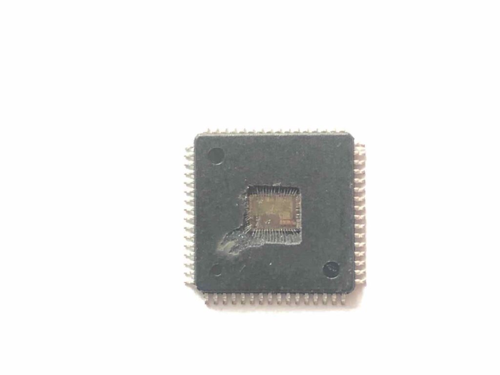
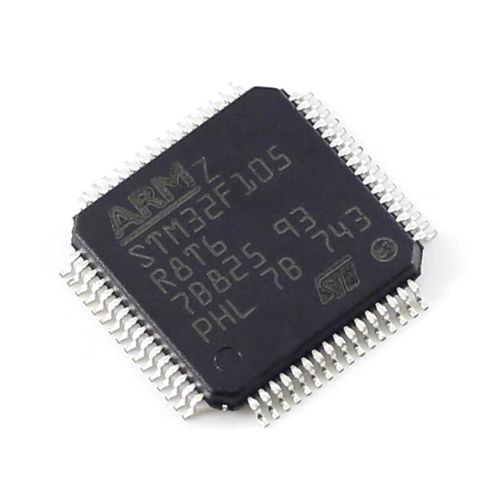
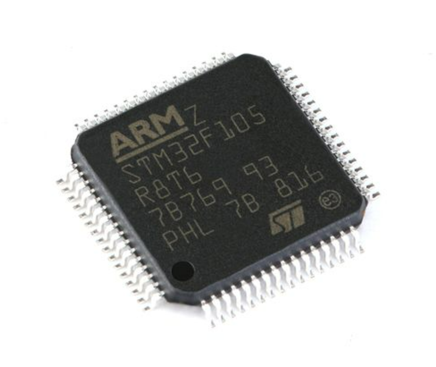
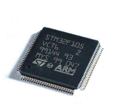
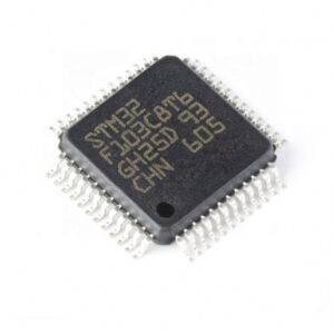
Replicate ARM MCU STM32F105R8T6 Embedded Flash Program
Replicate ARM MCU STM32F105R8T6 Embedded Flash Program and crack arm mcu protective fuse bit and then extract firmware from flash and eeprom memory of microprocessor;
The ARM Cortex™-M3 processor is the latest generation of ARM processors for embedded systems. It has been developed to provide a low-cost platform that meets the needs of MCU implementation, with a reduced pin count and low-power consumption, while delivering outstanding computational performance and an advanced system response to interrupts of arm microcontroller stm32f105vct flash memory content decrypting.
The ARM Cortex™-M3 32-bit RISC processor features exceptional code-efficiency, delivering the high-performance expected from an ARM core in the memory size usually associated with 8- and 16-bit devices.
extract arm microprocessor stm32f105r8 source code from flash memory
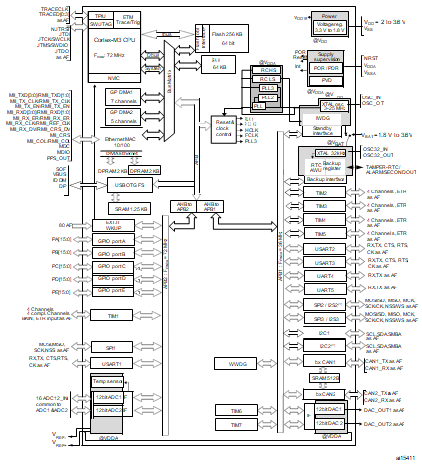
With its embedded ARM core, STM32F105xx and STM32F107xx connectivity line family is compatible with all ARM tools and software. below Figure shows the general block diagram of the device family.
répliquer le programme flash intégré du MCU ARM STM32F105R8T6 et le bit de fusible de protection du MCU Crack Arm, puis extraire le micrologiciel de la mémoire flash et de la mémoire eeprom du microprocesseur ;
Decrypt ARM Microcontroller STM32F105VCT Secured Memory Binary Program
Decrypt ARM Microcontroller STM32F105VCT Secured Memory Binary Program is a process to unlock mcu stm32f105vct tamper resistance system, and then copy firmware from microprocessor;
Features
Core: ARM 32-bit Cortex™-M3 CPU
– 72 MHz maximum frequency, 1.25 DMIPS/MHz (Dhrystone 2.1) performance at 0 wait state memory
LQFP100 14 × 14 mm
LQFP64 10 × 10 mm access
– Single-cycle multiplication and hardware division Memories
– 64 to 256 Kbytes of Flash memory
– up to 64 Kbytes of general-purpose SRAM
Clock, reset and supply management
– 2.0 to 3.6 V application supply and I/Os
– POR, PDR, and programmable voltage detector (PVD)
– 3-to-25 MHz crystal oscillator
– Internal 8 MHz factory-trimmed RC
– Internal 40 kHz RC with calibration
– 32 kHz oscillator for RTC with calibration Low power
– Sleep, Stop and Standby modes
– VBAT supply for RTC and backup registers 2 × 12-bit, 1 µs A/D converters (16 channels)
– Conversion range: 0 to 3.6 V
– Sample and hold capability
– Temperature sensor
– up to 2 MSPS in interleaved mode 2 × 12-bit D/A converters
DMA: 12-channel DMA controller
– Supported peripherals: timers, ADCs, DAC, I2Ss, SPIs, I2Cs and USARTs
Up to 10 timers with pinout remap capability
descifrar el microcontrolador ARM STM32F105VCT6 programa binario de memoria segura es un proceso para desbloquear el sistema de resistencia a manipulaciones MCU STM32F105VCT y luego copiar el firmware del microprocesador;
– Up to four 16-bit timers, each with up to 4 IC/OC/PWM or pulse counter and quadrature (incremental) encoder input
– 1 × 16-bit motor control PWM timer with dead-time generation and emergency stop
– 2 × watchdog timers (Independent and Window)
– SysTick timer: a 24-bit downcounter
– 2 × 16-bit basic timers to drive the DAC
Up to 14 communication interfaces with pinout remap capability
– Up to 2 × I2C interfaces (SMBus/PMBus)
– Up to 5 USARTs (ISO 7816 interface, LIN,
IrDA capability, modem control)
– Up to 3 SPIs (18 Mbit/s), 2 with a multiplexed I2S interface that offers audio class accuracy via advanced PLL schemes
décrypter le microcontrôleur ARM STM32F105VCT6 programme binaire de mémoire sécurisée est un processus permettant de déverrouiller le système de résistance à l’effraction MCU STM32F105VCT, puis de copier le micrologiciel du microprocesseur ;
– 2 × CAN interfaces (2.0B Active) with 512 bytes of dedicated SRAM
– USB 2.0 full-speed device/host/OTG controller with on-chip PHY that supports HNP/SRP/ID with 1.25 Kbytes of dedicated SRAM
– 10/100 Ethernet MAC with dedicated DMA and SRAM (4 Kbytes): IEEE1588 hardware support, MII/RMII available on all packages
– Serial wire debug (SWD) & JTAG interfaces
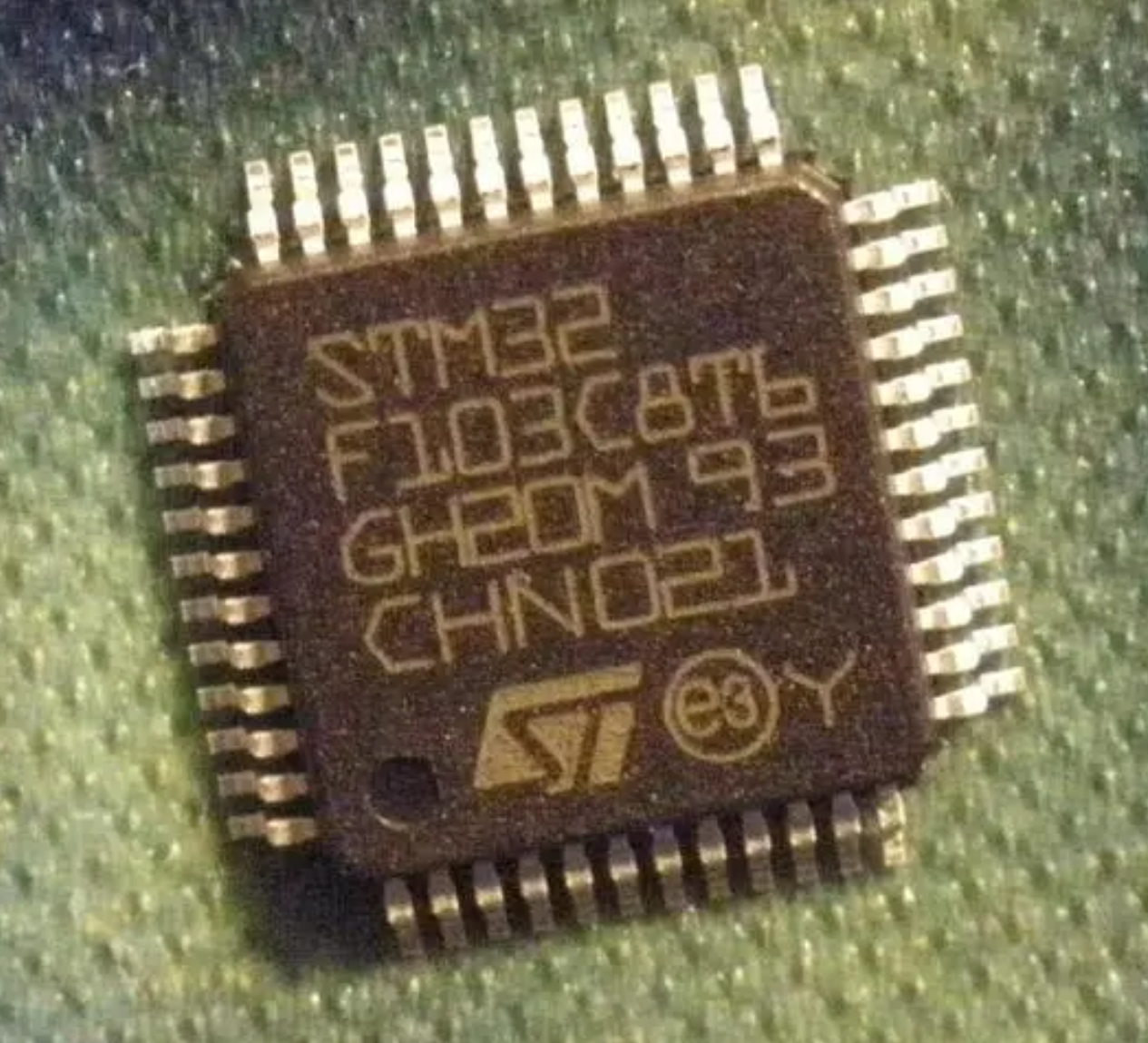
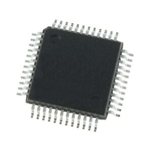
Restore Microcontroller STM32F103C8 Flash Program Code
Restore Microcontroller STM32F103C8 Flash Program Code and copy extracted firmware to new MCU in order to make STM32F103C8 binary code microprocessor cloning;
The current consumption of the on-chip peripherals is given in Table 18. The process of Recover MCU is placed under the following conditions:
restaurar o microcontrolador STM32F103C8 código do programa flash e copiar o firmware extraído para o novo MCU, a fim de fazer STM32F103C8 clonagem de microprocessador de código binário;
- l all I/O pins are in input mode with a static value at VDD or VSS (no load)
- l all peripherals are disabled unless otherwise mentioned
- l the given value is calculated by measuring the current consumption
- – with all peripherals clocked off
- – with only one peripheral clocked on
- l ambient operating temperature and VDD supply voltage conditions summarized
External clock source characteristics includes below points:
In a given sampling window, either three or six samples of the input signal are taken to determine the validity of the signal. This is determined by the value written to GPxQSELn register to recover stmicro stm32f103c6 mcu flash content.
ripristinare il microcontrollore STM32F103C8 il codice del programma flash e copiare il firmware estratto sul nuovo MCU per effettuare STM32F103C8 clonazione del microprocessore in codice binario;
Case 1:
Qualification using three samples
Sampling window width = (SYSCLKOUT cycle × 2 × QUALPRD) × 2, if QUALPRD ≠ 0 Sampling window width = (SYSCLKOUT cycle) × 2, if QUALPRD = 0
casser données heximales eeprom du microcontrôleur stm32f103c8,
Case 2:
Qualification using six samples Sampling window width = (SYSCLKOUT cycle × 2 × QUALPRD) × 5, if QUALPRD ≠ 0 Sampling window width = (SYSCLKOUT cycle) × 5, if QUALPRD = 0
копировать зашифрованная программа встроенной прошивки MCU stm32f103c8 IC,
Recover STMicro STM32F103C6 MCU Flash Full Content
Recover STMicro STM32F103C6 MCU Flash Full Content needs to unlock arm microcontroller stm32f103c6 memory and then copy extracted firmware to fresh MCU for cloning purpose;
The current consumption is a function of several parameters and factors such as the operating voltage, ambient temperature, I/O pin loading, device software configuration, operating frequencies, I/O pin switching rate, program location in memory and executed binary code extracted.
The current consumption is measured as described in Figure 11: Current consumption measurement scheme.
All Run-mode current consumption measurements given in this section are performed with a reduced code that gives a consumption equivalent to Dhrystone 2.1 code for the purpose of restoring microcontroller stm32f103c4 flash source code.
brechen stm32f103c6 Mikrocontroller-Flash-Speicher-Binärdatei,
The MCU is placed under the following conditions:
- l All I/O pins are in input mode with a static value at VDD or VSS (no load)
- l All peripherals are disabled except if it is explicitly mentioned
- l Prefetch in on (reminder: this bit must be set before clock setting and bus prescaling)
- l When the peripherals are enabled fPCLK1 = fHCLK, fPCLK2 = fHCLK
The parameters given in below Table are derived from tests performed under the ambient temperature and VDD supply voltage conditions summarized.
The Recovering MCU is placed under the following conditions:
brechen stm32f103c6 Mikroprozessor-Flash- und EEPROM-Heximalprogramm,
- All I/O pins are in input mode with a static value at VDD or VSS (no load)
- All peripherals are disabled except if it is explicitly mentioned
- When the peripherals are enabled fPCLK1 = fHCLK, fPCLK2 = fHCLK, fADCCLK = fPCLK2/2