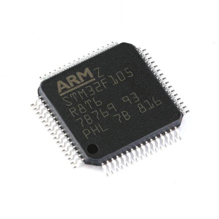
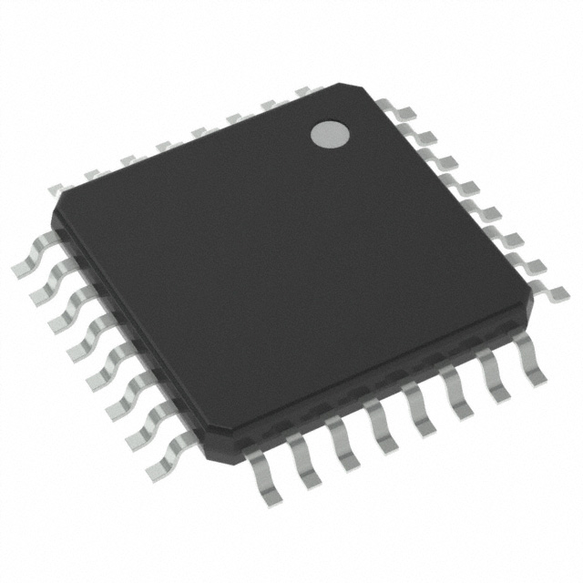
 Reverse Engineering ARM Microprocessor STM32F103RB Flash Memory
Reverse Engineering ARM Microprocessor STM32F103RB Flash Memory is a process to crack stm32f103rb secured microcontroller fuse bit and copy the heximal memory firmware to new microcomputer stm32f103rb flash memory;
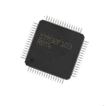
Reverse Engineering ARM Microprocessor STM32F103RB Flash Memory is a process to crack stm32f103rb secured microcontroller fuse bit and copy the heximal memory firmware to new microcomputer stm32f103rb flash memory
The device has an integrated power-on reset (POR) / power-down reset (PDR) circuitry. It is always active, and ensures proper operation starting from/down to 2 V to pull out stm32f103t8 microcontroller flash data. The device remains in reset mode when VDD is below a specified threshold, VPOR/PDR, without the need for an external reset circuit.
The device features an embedded programmable voltage detector (PVD) that monitors the VDD/VDDA power supply and compares it to the VPVD threshold. An interrupt can be generated when VDD/VDDA drops below the VPVD threshold and/or when VDD/VDDA is higher than the VPVD threshold. The interrupt service routine can then generate a warning message and/or put the MCU into a safe state. The PVD is enabled by software.
unlock STM32F103RB arm microcontroller fuse bit and readout firmware heximal of flash memory of mcu stm32f103rb
The regulator has three operation modes: main (MR), low-power (LPR) and power down.
- MR is used in the nominal regulation mode (Run)
- LPR is used in the Stop mode
- Power down is used in Standby mode: the regulator output is in high impedance: the kernel circuitry is powered down, inducing zero consumption (but the contents of the registers and SRAM are lost)
This regulator is always enabled after reset. It is disabled in Standby mode, providing high impedance output. The STM32F103xx performance line supports three low-power modes to achieve the best compromise between low-power consumption, short startup time and available wakeup sources:
- Sleep mode
In Sleep mode, only the CPU is stopped. All peripherals continue to operate and can wake up the CPU when an interrupt/event occurs.
- Stop mode
The Stop mode achieves the lowest power consumption while retaining the content of SRAM and registers. All clocks in the 1.8 V domain are stopped by cracking stm32f103vet7 arm ic mcu flash memory, the PLL, the HSI RC and the HSE crystal oscillators are disabled. The voltage regulator can also be put either in normal or in low-power mode.
desbloquee la broca del fusible del microcontrolador del brazo STM32F103RB y lea el firmware heximal de la memoria flash de mcu stm32f103rb
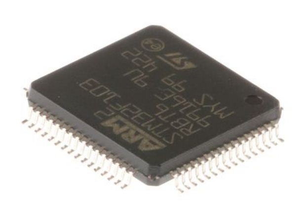
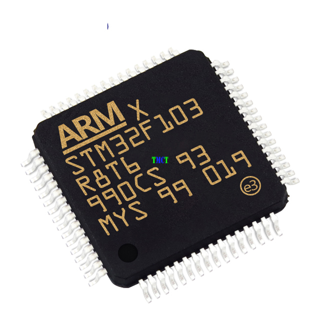
Reverse Engineering STM32F103R8 Microcomputer Flash Program
Reverse Engineering STM32F103R8 Microcomputer Flash Program can help engineer to extract embedded firmware heximal file from secured mcu stm32f103r8 then clone arm microcontroller stm32f103r8 binary data to new Microprocessor;
Reverse Engineering STM32F103R8 Microcomputer Flash Program can help engineer to extract embedded firmware heximal file from secured mcu stm32f103r8 then clone arm microcontroller stm32f103r8 binary data to new Microprocessor
System clock selection is performed on startup, however the internal RC 8 MHz oscillator is selected as default CPU clock on reset. An external 4-16 MHz clock can be selected, in which case it is monitored for failure. If failure is detected, the system automatically switches back to the internal RC oscillator when restoring stm32f103c4 arm microcontroller flash binary file. A software interrupt is generated if enabled. Similarly, full interrupt management of the PLL clock entry is available when necessary (for example on failure of an indirectly used external crystal, resonator or oscillator).
Several prescalers allow the configuration of the AHB frequency, the high-speed APB (APB2) and the low-speed APB (APB1) domains. The maximum frequency of the AHB and the high-speed APB domains is 72 MHz. The maximum allowed frequency of the low-speed APB domain is 36 MHz. See Figure 2 for details on the clock tree.
unlock secured STM32F105R8T6 microcontroller fuse bit and extract heximal program file from STM32F105R8T6 microprocessor flash memory
At startup, boot pins are used to select one of three boot options:
- Boot from user Flash
- Boot from System memory
- Boot from embedded SRAM
The boot loader is located in System memory. It is used to reprogram the Flash memory by using USART1. For further details refer to AN2606, available on www.st.com.
- VDD = 2.0 to 3.6 V: external power supply for I/Os and the internal regulator. Provided externally through VDD
- VSSA, VDDA = 2.0 to 3.6 V: external analog power supplies for ADC, reset blocks, RCs and PLL (minimum voltage to be applied to VDDA is 2.4 V when the ADC is used) by restoring stm32f103c8 microcontroller flash program code. VDDA and VSSA must be connected to VDD and VSS,
- VBAT = 8 to 3.6 V: power supply for RTC, external clock 32 kHz oscillator and backup registers (through power switch) when VDD is not present.
For more details on how to connect power pins, refer to Figure 14: Power supply scheme.
El programa flash de microcomputadora STM32F103R8 de ingeniería inversa puede ayudar al ingeniero a extraer el archivo heximal del firmware integrado de mcu stm32f103r8 seguro y luego clonar los datos binarios del microcontrolador stm32f103r8 del brazo al nuevo microprocesador
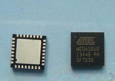
Break Locked ATmega32U2 Microprocessor Flash
Break Locked ATmega32U2 Microprocessor Flash and copy heximal firmware to new atmega32u2 flash memory and eeprom memory, the source code of binary program and data will be pull out from original master mcu atmega32u2;
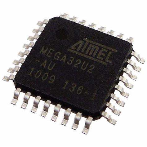
Break Locked ATmega32U2 Microprocessor Flash and copy heximal firmware to new atmega32u2 flash memory and eeprom memory, the source code of binary program and data will be pull out from original master mcu atmega32u2
Input to the inverting Oscillator amplifier and input to the internal clock operating circuit. Output from the inverting Oscillator amplifier if enabled by Fuse. Also serves as a generic I/O. This documentation contains simple code examples that briefly show how to use various parts of the device. Be aware that not all C compiler vendors include bit definitions in the header files and interrupt handling in C is compiler dependent. Please confirm with the C compiler documen- tation for more details.
These code examples assume that the part specific header file is included before compilation. For I/O registers located in extended I/O map, “IN”, “OUT”, “SBIS”, “SBIC”, “CBI”, and “SBI” instructions must be replaced with instructions that allow access to extended I/O. Typically “LDS” and “STS” combined with “SBRS”, “SBRC”, “SBR”, and “CBR”. Reliability Qualification results show that the projected data retention failure rate is much less than 1 PPM over 20 years at 85°C or 100 years at 25°C.
reverse engineering ATMEGA32U2 secured mcu fuse bit and dump firmware binary or heximal out of ATMEGA32U2 flas memory
This section discusses the AVR core architecture in general. The main function of the CPU core is to ensure correct program execution. The CPU must therefore be able to access memories when reversing atmega16u2 microcontroller protection, perform calculations, control peripherals, and handle interrupts.
Break Locked ATmega32U2 Microprocesador Flash y copie el firmware heximal a la nueva memoria flash atmega32u2 y memoria eeprom, el código fuente del programa binario y los datos se extraerán del mcu maestro original atmega32u2
In order to maximize performance and parallelism, the AVR uses a Harvard architecture – with separate memories and buses for program and data. Instructions in the program memory are executed with a single level pipelining. While one instruction is being executed, the next instruction is prefetched from the program memory after recovering atmega8u2 encrypted microprocessor flash memory. This concept enables instructions to be executed in every clock cycle. The program memory is In-System Reprogrammable Flash memory.
Reverse AVR Microcomputer ATmega16U2 Flash Program
Reverse AVR Microcomputer ATmega16U2 Flash Program and copy atmel avr mcu atmega16u2 firmware to new microcontroller, the heximal firmware of original atmega16u2 microprocessor can be restored;
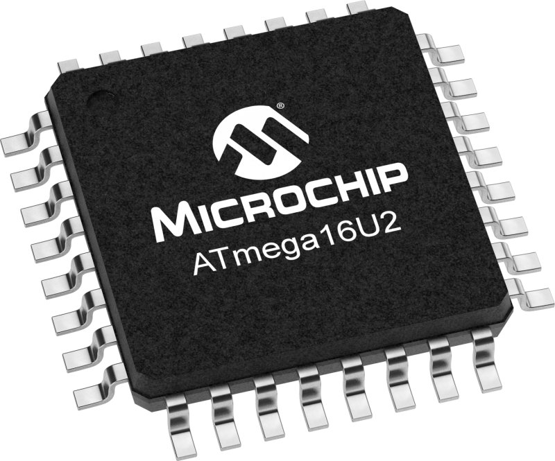
Reverse AVR Microcomputer ATmega16U2 Flash Program and copy atmel avr mcu atmega16u2 firmware to new microcontroller, the heximal firmware of original atmega16u2 microprocessor can be restored
The ATmega8U2/16U2/32U2 are supported with a full suite of program and system develop- ment tools including: C compilers, macro assemblers, program debugger/simulators, in-circuit emulators, and evaluation kits.
AVCC is the supply voltage pin (input) for all analog features (Analog Comparator, PLL). It should be externally connected to VCC through a low-pass filter.
Port B is an 8-bit bi-directional I/O port with internal pull-up resistors (selected for each bit). The Port B output buffers have symmetrical drive characteristics with both high sink and source capability. As inputs, Port B pins that are externally pulled low will source current if the pull-up resistors are activated. The Port B pins are tri-stated when a reset condition becomes active, even if the clock is not running.
crack secured mcu ATMEGA8U2
Port B also serves the functions of various special features of the ATmega8U2/16U2/32U2 as listed on page 74. Port D serves as analog inputs to the analog comparator.
Port D also serves as an 8-bit bi-directional I/O port, if the analog comparator is not used (con- cerns PD2/PD1 pins). Port pins can provide internal pull-up resistors (selected for each bit). The Port D output buffers have symmetrical drive characteristics with both high sink and source capability. As inputs, Port D pins that are externally pulled low will source current if the pull-up resistors are activated. The Port D pins are tri-stated when a reset condition becomes active, even if the clock is not running.
Reset input. A low level on this pin for longer than the minimum pulse length will generate a reset, even if the clock is not running. The minimum pulse length is given in “System Control and Reset” on page 47. Shorter pulses are not guaranteed to generate a reset. This pin alternatively serves as debugWire channel or as generic I/O. The configuration depends on the fuses RST- DISBL and DWEN.
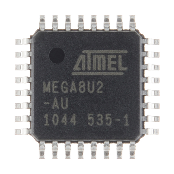
Recover Secured MCU ATmega8U2 Flash Heximal
Recover Secured MCU ATmega8U2 Flash Heximal after unlock atmega8 microcontroller flash memory protection and extract avr chip atmega8u2 binary code from its flash and eeprom memory;

Recover Secured MCU ATmega8U2 Flash Heximal after unlock atmega8 microcontroller flash memory protection and extract avr chip atmega8u2 binary code from its flash and eeprom memory
The Power-down mode saves the register contents but freezes the Oscillator, disabling all other chip functions until the next interrupt or Hardware Reset. In Standby mode, the Crystal/Resonator Oscillator is running while the rest of the device is sleeping when pulling flash content of microchip atmega8u2 mcu memory. This allows very fast start-up combined with low power consumption. In Extended Standby mode, the main Oscillator continues to run.
crack atmega8u2 microcontroller fuse bit and extract embedded firmware from flash memory
The device is manufactured using Atmel’s high-density nonvolatile memory technology. The on- chip ISP Flash allows the program memory to be reprogrammed in-system through an SPI serial interface, by a conventional nonvolatile memory programmer, or by an on-chip Boot program running on the AVR core. The boot program can use any interface to download the application program in the application Flash memory when restoring atmega8l microcomputer flash data. Software in the Boot Flash section will continue to run while the Application Flash section is updated, providing true Read-While-Write operation. By combining an 8-bit RISC CPU with In-System Self-Programmable Flash on a monolithic chip, the Atmel ATmega8U2/16U2/32U2 is a powerful microcontroller that provides a highly flexible and cost effective solution to many embedded control applications.
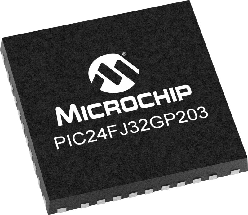
Microchip PIC24FJ32GP203 MCU Flash Memory Heximal Restoration
Microchip PIC24FJ32GP203 MCU Flash Memory Heximal Restoration including unlocking PIC24FJ32GP203 MCU program memory and extract pic24fj32gp203 secured microcontroller flash memory source code;
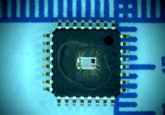
Microchip PIC24FJ32GP203 MCU Flash Memory Heximal Restoration including unlocking PIC24FJ32GP203 MCU program memory and extract pic24fj32gp203 secured microcontroller flash memory source code
In recent years, large value, low-voltage, surface-mount ceramic capacitors have become very cost-effective in sizes up to a few tens of microfarad. The low-ESR, small physical size and other properties make ceramic capacitors very attractive in many types of applications.
Ceramic capacitors are suitable for use with the internal voltage regulator of this microcontroller. However, some care is needed in selecting the capacitor to ensure that it maintains sufficient capacitance over the intended operating range of the application.
Typical low-cost, 10 μF ceramic capacitors are available in X5R, X7R and Y5V dielectric ratings (other types are also available, but are less common). The initial tolerance specifications for these types of capacitors are often specified as ±10% to ±20% (X5R and X7R) or -20%/+80% (Y5V) when breaking pic24fj16ga002 microcontroller flash memory heximal. However, the effective capacitance that these capacitors provide in an application circuit will also vary based on additional factors, such as the applied DC bias voltage and the temperature. The total in-circuit tolerance is, therefore, much wider than the initial tolerance specification.
unlock locked microprocessor PIC24FJ32GP203 memory and readout embedded firmware code from microcontroller chip PIC24FJ32GP203 flash memory
The X5R and X7R capacitors typically exhibit satisfactory temperature stability (ex: ±15% over a wide temperature range, but consult the manufacturer’s data sheets for exact specifications). However, Y5V capacitors typically have extreme temperature tolerance specifications of +22%/-82% when recover pic24fj32gp202 mcu flash memory program. Due to the extreme temperature tolerance, a 10 μF nominal rated Y5V type capacitor may not deliver enough total capacitance to meet minimum internal voltage regulator stability and transient response requirements. Therefore, Y5V capacitors are not recommended for use with the internal regulator if the application must operate over a wide temperature range.
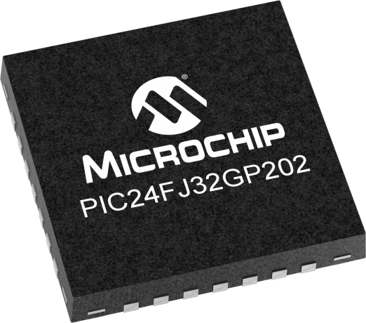
Recover Secured MCU PIC24FJ32GP202 Flash Program
Recover Secured MCU PIC24FJ32GP202 Flash Program from its memory needs to crack microcontroller pic24fj32gp202 flash memory and extract source code from pic24fj32gp202 microprocessor flash memory;
Recover Secured MCU PIC24FJ32GP202 Flash Program from its memory needs to crack microcontroller pic24fj32gp202 flash memory and extract source code from pic24fj32gp202 microprocessor flash memory
During programming and debugging, the resistance and capacitance that can be added to the pin must be considered. Device programmers and debuggers drive the MCLR pin. Consequently, specific voltage levels (VIH and VIL) and fast signal transitions must not be adversely affected. Therefore, specific values of R1 and C1 will need to be adjusted based on the application and PCB requirements.
For example, it is recommended that the capacitor, C1, be isolated from the MCLR pin during programming and debugging operations by using a jumper when executing microcontroller pic24fj16ga002 software decryption. The jumper is replaced for normal run-time operations. Any components associated with the MCLR pin should be placed within 0.25 inch (6 mm) of the pin.
- R1 ≤ 10 kΩ is A suggested starting value is 10 kΩ. Ensure that the MCLR pin VIH and VIL specifications are met.
- R2 ≤ 470Ω will limit any current flowing into MCLR from the external capacitor, C, in the event of a MCLR pin breakdown, due to Electrostatic Discharge (ESD) or Electrical Overstress (EOS). Ensure that the MCLR pin VIH and VIL specifications are met;
A low-ESR (< 5Ω) capacitor is required on the VCAP pin to stabilize the voltage regulator output voltage. The VCAP pin must not be connected to VDD and must use a capacitor of 10 µF connected to ground to break microcontroller pic24fj16ga002 flash memory heximal program. The type can be ceramic or tantalum. Suitable examples of capacitors are shown in Table 2-1. Capacitors with equivalent specifications can be used.
crack secured microcontroller PIC24FJ32GP202 and readout mcu chip PIC24FJ32GP202 flash memory program and eeprom memory data
Designers may use Figure 2-3 to evaluate the ESR equivalence of candidate devices. The placement of this capacitor should be close to VCAP. It is recommended that the trace length not exceed 0.25 inch (6 mm). Refer to 27.4 On-Chip Voltage Regulator for additional information.
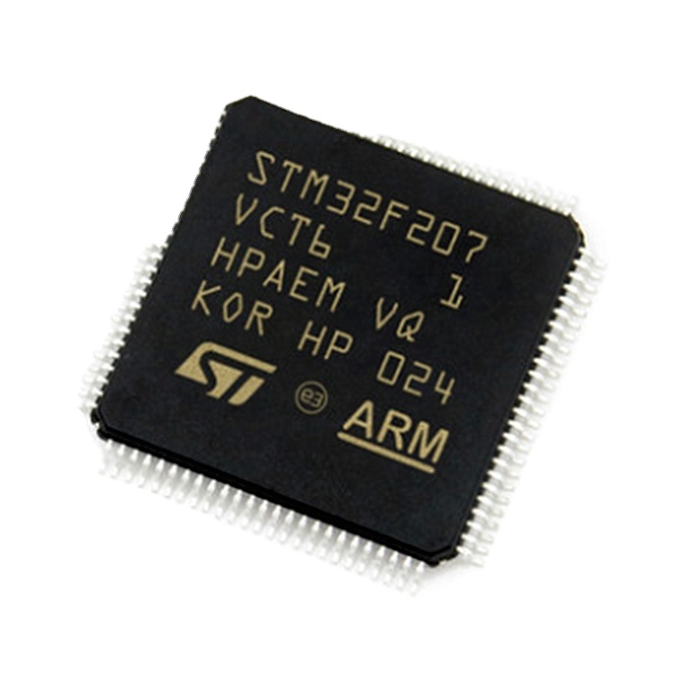
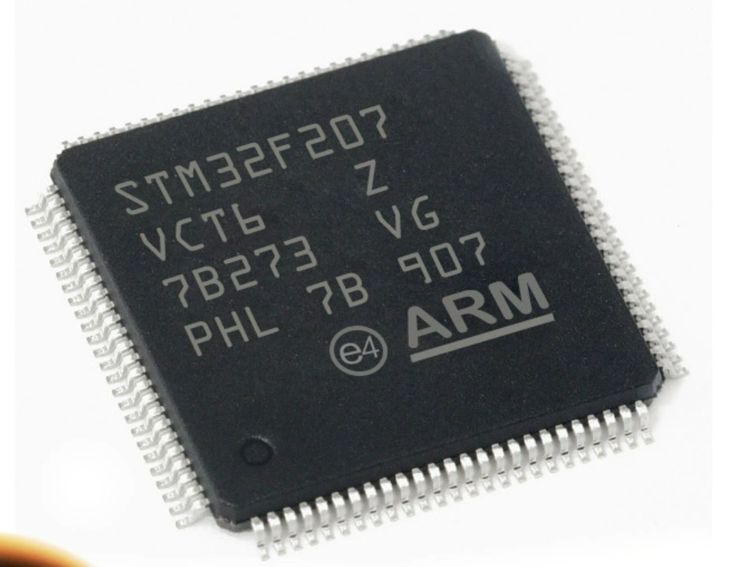
Reverse Secured STM32F207VCT6 Microprocessor Flash Heximal
Reverse Secured STM32F207VCT6 Microprocessor Flash Heximal and dump embedded firmware from stm32f207vct6 flash memory, extract source code from stm32f207vct6 flash memory;
Reverse Secured STM32F207VCT6 Microprocessor Flash Heximal and dump embedded firmware from stm32f207vct6 flash memory, extract source code from stm32f207vct6 flash memory;
Peripheral available only on STM32F207xx devices.
The STM32F207xx devices provide an IEEE-802.3-2002-compliant media access controller (MAC) for Ethernet LAN communications through an industry-standard medium- independent interface (MII) or a reduced medium-independent interface (RMII).
The STM32F207xx requires an external physical interface device (PHY) to connect to the physical LAN bus (twisted-pair, fiber, etc.). the PHY is connected to the STM32F207xx MII port using 17 signals for MII or 9 signals for RMII, and can be clocked using the 25 MHz (MII) or 50 MHz (RMII) output from the STM32F207xx by restoring stm32f205zct6 locked mcu chip memory content.
obrnuti inženjer osigurao STM32F207VCT6 mikroprocesorski sustav otpora neovlaštenog mijenjanja i program za flash memoriju za očitavanje i softver iz otključanog mikrokontrolera STM32F207VCT6 kopirati ugrađeni firmware izvornog koda na novi STM32F207VCT6 zaštitni MCU čip,
The STM32F207xx includes the following features:
Supports 10 and 100 Mbit/s rates
Dedicated DMA controller allowing high-speed transfers between the dedicated SRAM and the descriptors (see the STM32F20x and STM32F21x reference manual for details)
Tagged MAC frame support (VLAN support)
Half-duplex (CSMA/CD) and full-duplex operation
MAC control sublayer (control frames) support
32-bit CRC generation and removal
inżynieria wsteczna zabezpieczony STM32F207VCT6 mikroprocesorowy system odporności na manipulacje oraz odczyt programu pamięci flash i oprogramowania z odblokowanego mikrokontrolera STM32F207VCT6 kopiowania wbudowanego oprogramowania układowego kodu źródłowego do nowego STM32F207VCT6 ochronnego układu MCU,
Several address filtering modes for physical and multicast address (multicast and group addresses)
32-bit status code for each transmitted or received frame
Internal FIFOs to buffer transmit and receive The transmit FIFO and the receive FIFO are both 2 Kbytes (4 Kbytes in total)
Supports hardware PTP (precision time protocol) in accordance with IEEE 1588 2008 (PTP V2) with the time stamp comparator connected to the TIM2 input
Triggers interrupt when system time becomes greater than target time
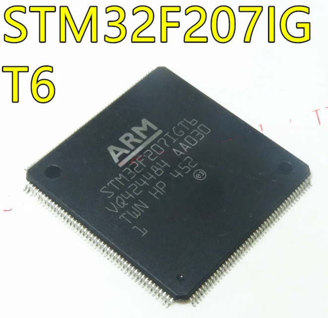
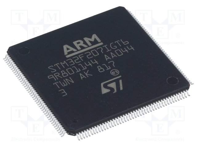
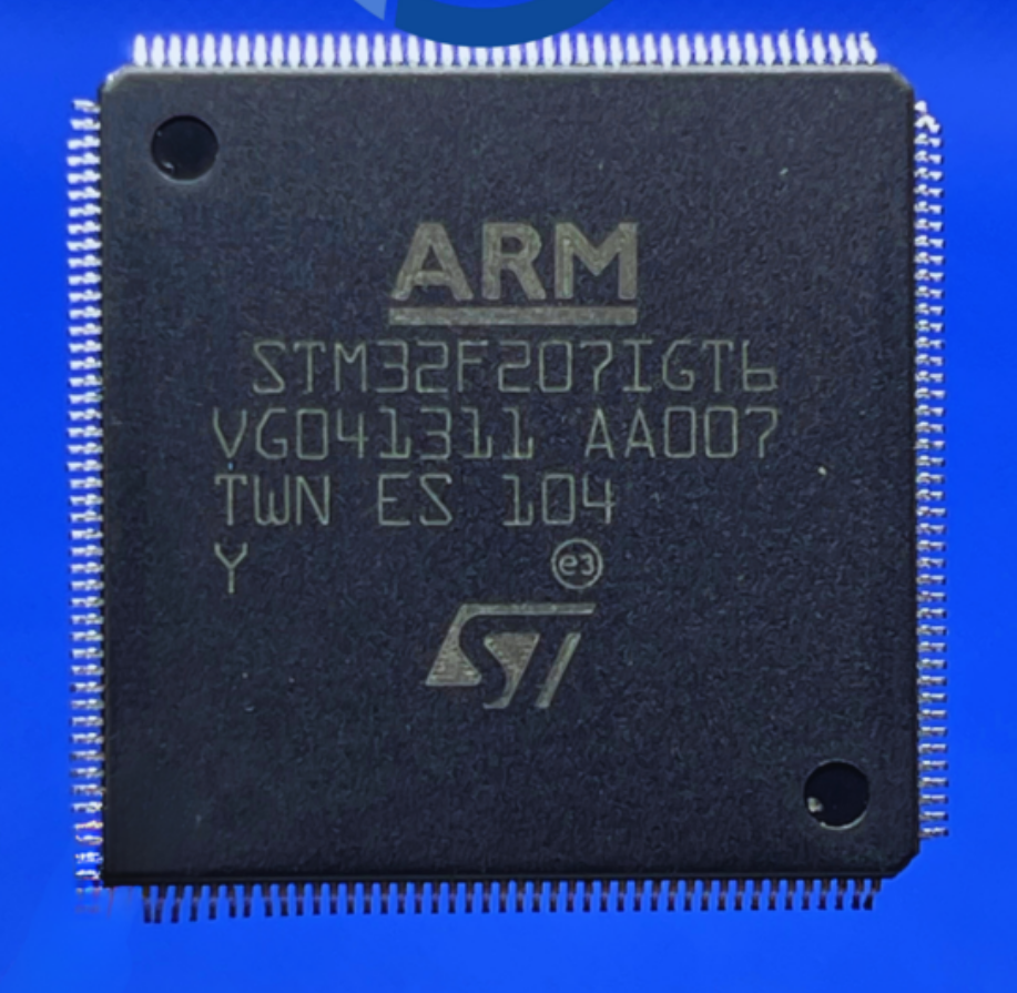
ARM Microcontroller STM32F207IGT6 Flash Firmware Recovery
ARM Microcontroller STM32F207IGT6 Flash Firmware Recovery needs to crack protected MCU STM32F207IGT6 protective system then copy embedded flash content from STM32F207IGT6 MCU memory;
ARM Microcontroller STM32F207IGT6 Flash Firmware Recovery needs to crack protected MCU STM32F207IGT6 protective system then copy embedded flash content from STM32F207IGT6 MCU memory
USART1, USART2, USART3 and USART6 also provide hardware management of the CTS and RTS signals, Smart Card mode (ISO 7816 compliant) and SPI-like communication capability. All interfaces can be served by the DMA controller.
Odzyskiwanie wbudowanego oprogramowania układowego z mikrokontrolerem zabezpieczonym STM32F207IGT6 pamięcią flash ARM musi złamać chroniony system ochronny MCU STM32F207IGT6, a następnie skopiować osadzoną zawartość flash danych binarnych lub programu szesnastkowego z STM32F207IGT6 oryginalnej pamięci mikroprocesora głównego
The STM32F20x devices feature up to three SPIs in slave and master modes in full-duplex and simplex communication modes. SPI1 can communicate at up to 30 Mbits/s, while SPI2 and SPI3 can communicate at up to 15 Mbit/s when breaking arm mcu stm32f205rbt6 flash memory. The 3-bit prescaler gives 8 master mode frequencies and the frame is configurable to 8 bits or 16 bits.
STMicroelectronics STM32F207IGT6 locked mcu fuse bit unlocking and extract embedded firmware heximal program from STMicroelectronics STM32F207IGT6 microprocessor flash memory
The hardware CRC generation/verification supports basic SD Card/MMC modes. All SPIs can be served by the DMA controller. The SPI interface can be configured to operate in TI mode for communications in master mode and slave mode. Two standard I2S interfaces (multiplexed with SPI2 and SPI3) are available. They can operate in master or slave mode, in half-duplex communication modes, and can be configured to operate with a 16-/32-bit resolution as input or output channels.
ARM osigurani mikrokontroler STM32F207IGT6 oporavak ugrađenog firmvera mora razbiti zaštićeni MCU STM32F207IGT6 zaštitni sustav, a zatim kopirati ugrađeni flash sadržaj binarnih podataka ili heksimalnog programa iz STM32F207IGT6 izvorne glavne mikroprocesorske memorije
Audio sampling frequencies from 8 kHz up to 192 kHz are supported. When either or both of the I2S interfaces is/are configured in master mode, the master clock can be output to the external DAC/CODEC at 256 times the sampling frequency. All I2Sx interfaces can be served by the DMA controller when recover embedded flash memory content from arm microcontroller stm32f205rct6.
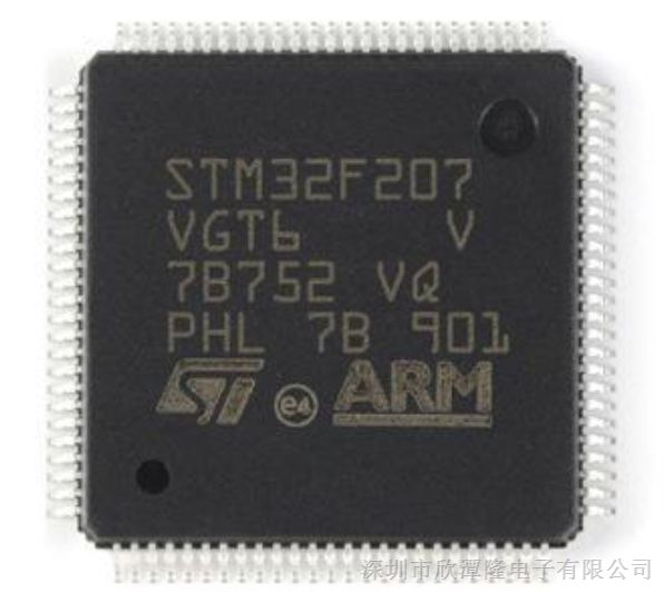
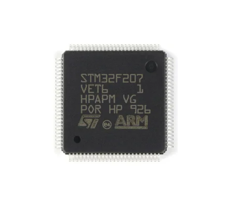
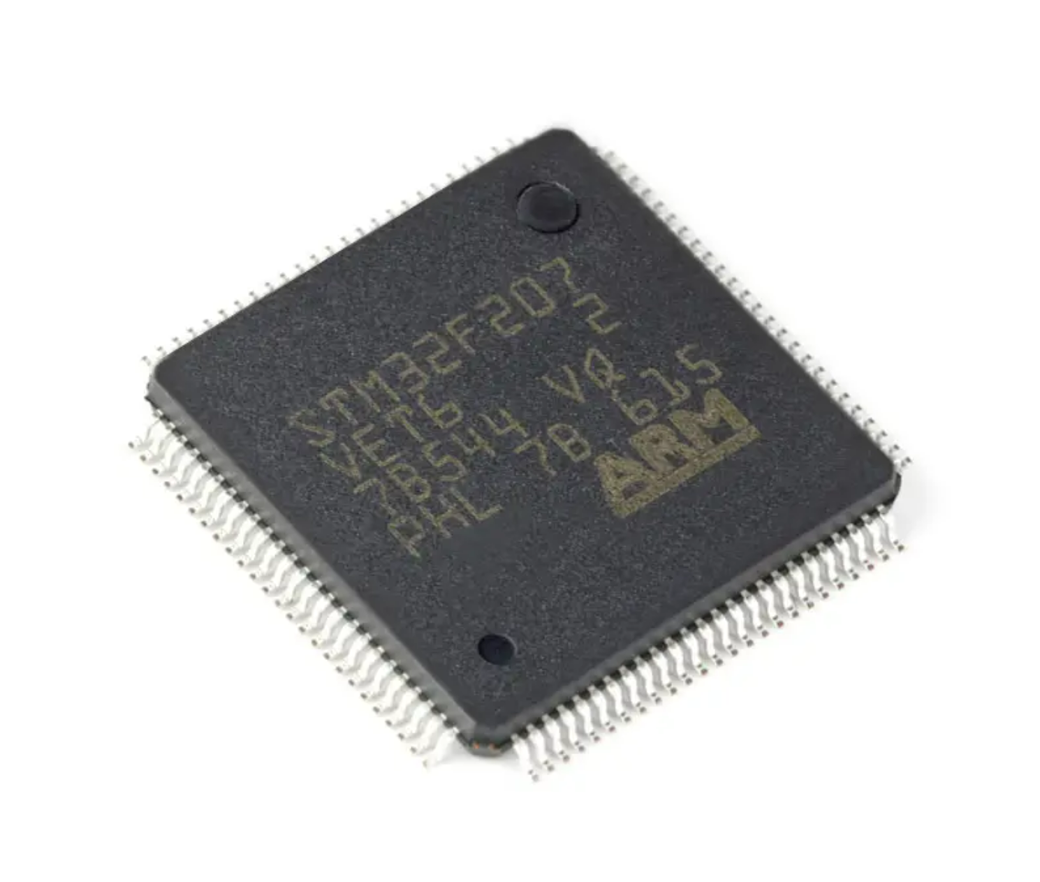
Locked STM32F207VET6 Microcontroller Firmware Code Restoration
Locked STM32F207VET6 Microcontroller Firmware Code Restoration is a process to crack protective stm32f207ve mcu flash memory then copy stm32f207vet6 mcu flash content to new microprocessor;
Locked STM32F207VET6 Microcontroller Firmware Code Restoration is a process to crack protective stm32f207ve mcu flash memory then copy stm32f207vet6 mcu flash content to new microprocessor;
These timers are based on a 16-bit auto-reload upcounter and a 16-bit prescaler. TIM10 and TIM11 feature one independent channel, whereas TIM9 has two independent channels for input capture/output compare, PWM or one-pulse mode output. They can be synchronized with the TIM2, TIM3, TIM4, TIM5 full-featured general-purpose timers. They can also be used as simple time bases.
Zaključana STM32F207VET6 mikrokontrolera Ugrađena obnova firmware koda postupak je za razbijanje zaštitne STM32F207VET6 MCU flash memorije, a zatim izdvajanje STM32F207VET6 šifriranog mikroprocesorskog flash sadržaja u formatu binarne datoteke ili heksimalnih podataka u novi mikroprocesor
These timers are based on a 16-bit auto-reload upcounter and a 16-bit prescaler. TIM13 and TIM14 feature one independent channel, whereas TIM12 has two independent channels for input capture/output compare to recover stm32f205rc microcontroller’s flash memory heximal, PWM or one-pulse mode output. They can be synchronized with the TIM2, TIM3, TIM4, TIM5 full-featured general-purpose timers.
They can also be used as simple time bases.
These timers are mainly used for DAC trigger and waveform generation. They can also be used as a generic 16-bit time base.
Przywracanie kodu oprogramowania układowego wbudowanego w mikrokontroler z zablokowanym STM32F207VET6 to proces polegający na złamaniu pamięci flash STM32F207VET6 ochronnej MCU, a następnie wyodrębnieniu STM32F207VET6 zaszyfrowanej zawartości flash mikroprocesora w formacie pliku binarnego lub danych szesnastkowych do nowego mikroprocesora
The independent watchdog is based on a 12-bit downcounter and 8-bit prescaler. It is clocked from an independent 32 kHz internal RC and as it operates independently from the main clock, it can operate in Stop and Standby modes. It can be used either as a watchdog to reset the device when a problem occurs, or as a free-running timer for application timeout.