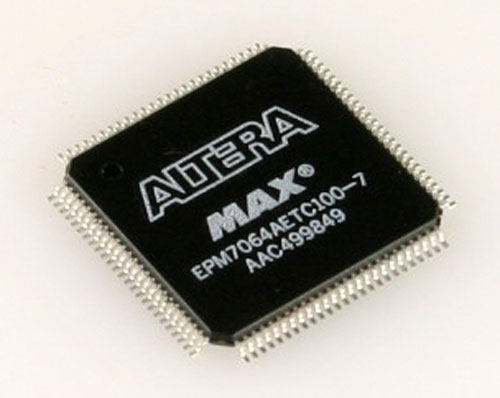
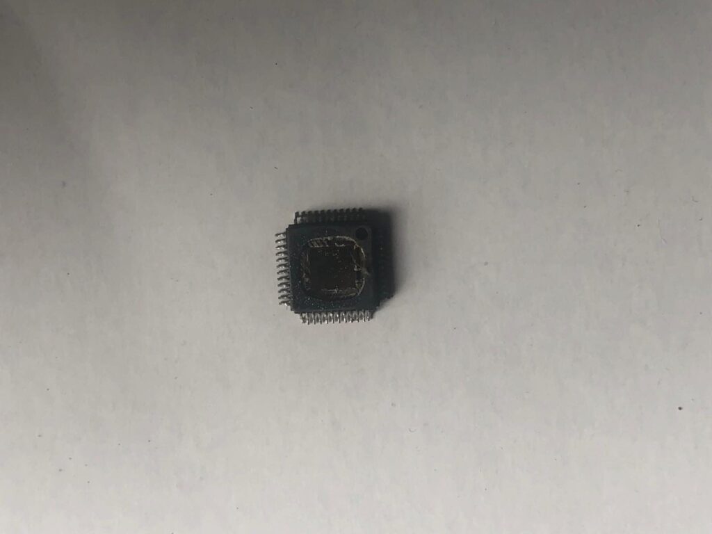
 Altera CPLD EPM7064AETC100 Chip Protection Breaking
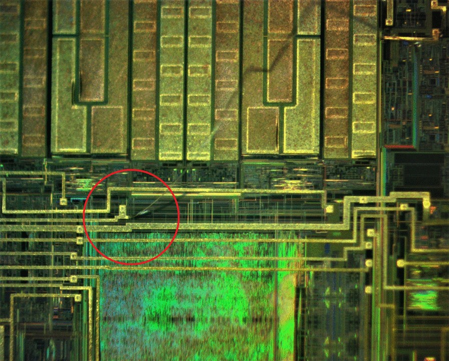
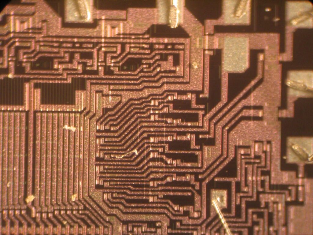
Altera CPLD EPM7064AETC100 Chip Protection Breaking needs to unlock epm7064aetc100 security fuse bit by focus ion beam and then copy embedded firmware from eeprom memory of cpld chip;
Bus-friendly architecture, including programmable slew-rate control
Open-drain output option
Programmable macrocell registers with individual clear, preset, clock, and clock enable controls
Programmable power-up states for macrocell registers in MAX 7000AE devices
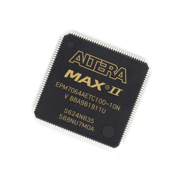
Altera CPLD EPM7064AETC100 захист мікросхеми від злому повинен розблокувати запобіжник безпеки epm7064aetc100 біт за променем focus ion beam, а потім скопіювати вбудовану прошивку з пам’яті eeprom чіпа cpld;
Programmable power-saving mode for 50% or greater power reduction in each macrocell
Configurable expander product-term distribution, allowing up to 32 product terms per macrocell
Programmable security bit for protection of proprietary designs 6 to 10 pin- or logic-driven output enable signals
Two global clock signals with optional inversion
Enhanced interconnect resources for improved routability
Fast input setup times provided by a dedicated path from I/O pin to macrocell registers
Programmable output slew-rate control from Crack PLD IC Altera EPM7064AETC100-4N
Programmable ground pins
Software design support and automatic place-and-route provided by Altera’s development systems for Windows-based PCs and Sun SPARCstation, and HP 9000 Series 700/800 workstations Additional design entry and simulation support provided by EDIF 2 0 0 and 3 0 0 netlist files, library of parameterized modules (LPM), Verilog HDL, VHDL, and other interfaces to popular EDA tools from manufacturers such as Cadence, Exemplar Logic, Mentor Graphics, OrCAD, Synopsys, Synplicity, and VeriBest.
Altera CPLD EPM7064AETC100 ruperea protecției cipului trebuie să deblocheze siguranța de securitate epm7064aetc100 bit cu fascicul de ioni de focalizare și apoi să copieze firmware-ul încorporat din memoria eeprom a cipului CPLD;
Programming support with Altera’s Master Programming Unit (MPU), MasterBlasterTM serial/universal serial bus (USB) communications cable, ByteBlasterMVTM parallel port download cable, and BitBlasterTM serial download cable, as well as programming hardware from third-party manufacturers and any JamTM STAPL File (.jam), Jam Byte-Code File (.jbc), or Serial Vector Format File (.svf) capable in-circuit tester when recover altera cpld epm7064aetc100 software.
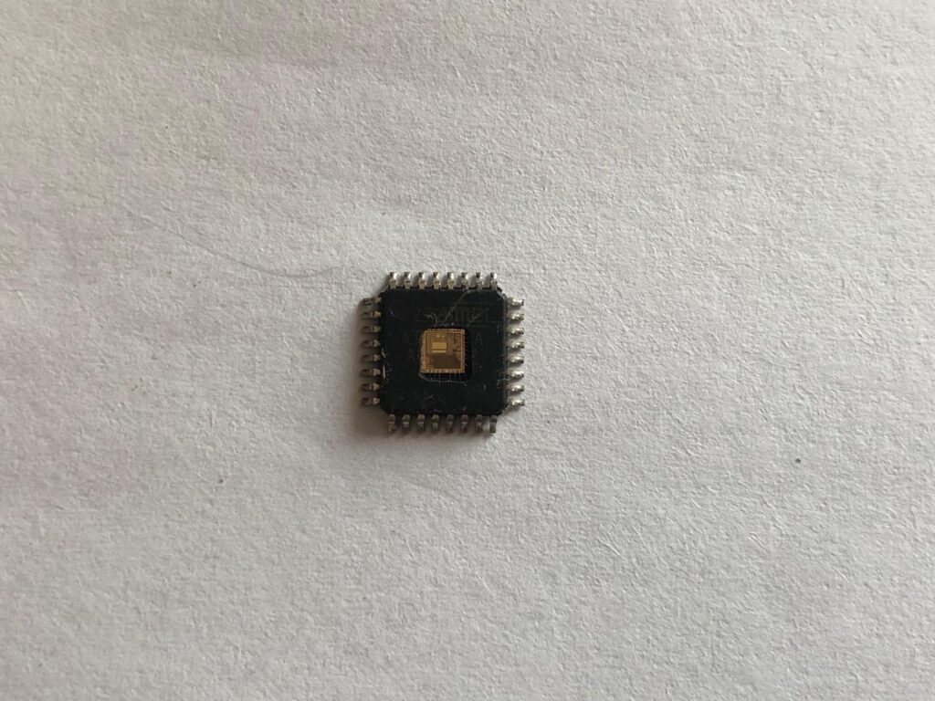
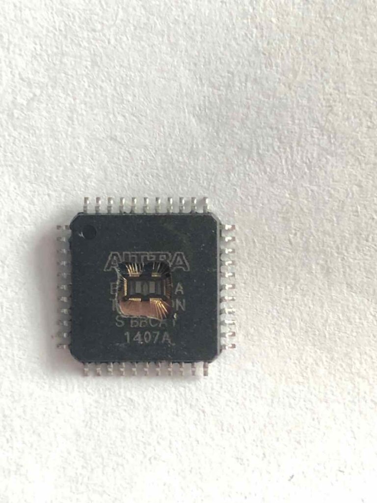
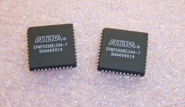
Reverse Engineering INTEL CPLD EPM7032AELC44-10N Chipset
Reverse Engineering INTEL CPLD EPM7032AELC44-10N Chipset can help engineer learn the internal structure of CPLD and unlock cpld epm7032 cpld through locating the fuse bit and disable it by focus ion beam, then the embedded jed file will be extracted from its eeprom directly;
High-performance 3.3-V EEPROM-based programmable logic devices (PLDs) built on second-generation Multiple Array MatriX (MAX®) architecture (see Table 1)
engenharia reversa Intel CPLD EPM7032AELC44-10N chipset pode ajudar o engenheiro aprender a estrutura interna do CPLD e desbloquear cpld epm7032 cpld através da localização do bit fusível e desativá-lo por feixe de íons de foco, então o arquivo jed incorporado será extraído de seu eeprom diretamente;
- 3.3-V in-system programmability (ISP) through the built-in IEEE Std. 1149.1 Joint Test Action Group (JTAG) interface with advanced pin-locking capability to reverse cpld epm7032aeti44 jed file
- MAX 7000AE device in-system programmability (ISP) circuitry compliant with IEEE Std. 1532
- EPM7128A and EPM7256A device ISP circuitry compatible with IEEE Std. 1532
- Built-in boundary-scan test (BST) circuitry compliant with IEEE Std. 1149.1
- Supports JEDEC Jam Standard Test and Programming Language (STAPL) JESD-71
- Enhanced ISP features
- Enhanced ISP algorithm for faster programming (excluding EPM7128A and EPM7256A devices)
- ISP_Done bit to ensure complete programming (excluding EPM7128A and EPM7256A devices)
리버스 엔지니어링 Intel CPLD EPM7032AELC44-10N 칩셋은 엔지니어가 CPLD의 내부 구조를 배우고 퓨즈 비트를 찾아 cpld epm7032 cpld의 잠금을 해제하고 초점 이온 빔으로 비활성화하면 임베디드 JED 파일이 eeprom에서 직접 추출됩니다.
-
- Pull-up resistor on I/O pins during in-system programming
- Pin-compatible with the popular 5.0-V MAX 7000S devices
- High-density PLDs ranging from 600 to 10,000 usable gates
- Extended temperature range
Recovering Altera CPLD EPM7032VTC44-15 Chipset Protection System
Recovering Altera CPLD EPM7032VTC44-15 Chipset Protection System is a process to crack altera cpld epm7032vtc44 security fuse bit and then copy embedded firmware out from its cpld flash memory;
4.5-ns pin-to-pin logic delays with counter frequencies of up to 227.3 MHz
MultiVoltTM I/O interface enables device core to run at 3.3 V, while I/O pins are compatible with 5.0-V, 3.3-V, and 2.5-V logic levels;
Pin counts ranging from 44 to 256 in a variety of thin quad flat pack (TQFP), plastic quad flat pack (PQFP), ball-grid array (BGA), space- saving FineLine BGATM, and plastic J-lead chip carrier (PLCC) packages;
Supports hot-socketing in MAX 7000AE devices
Programmable interconnect array (PIA) continuous routing structure for fast, predictable performance
PCI-compatible
Bus-friendly architecture, including programmable slew-rate control
Open-drain output option
Programmable macrocell registers with individual clear, preset, clock, and clock enable controls
Programmable power-up states for macrocell registers in MAX 7000AE devices
Programmable power-saving mode for 50% or greater power reduction in each macrocell
Configurable expander product-term distribution, allowing up to 32 product terms per macrocell
Programmable security bit for protection of proprietary designs which can be used to attack cpld chip encrypted code
6 to 10 pin- or logic-driven output enable signals
Two global clock signals with optional inversion
Enhanced interconnect resources for improved routability
Fast input setup times provided by a dedicated path from I/O pin to macrocell registers
Programmable output slew-rate control
Programmable ground pins which can be used to copy lattice cpld program file
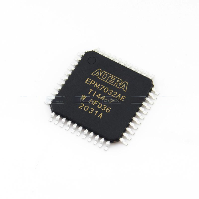
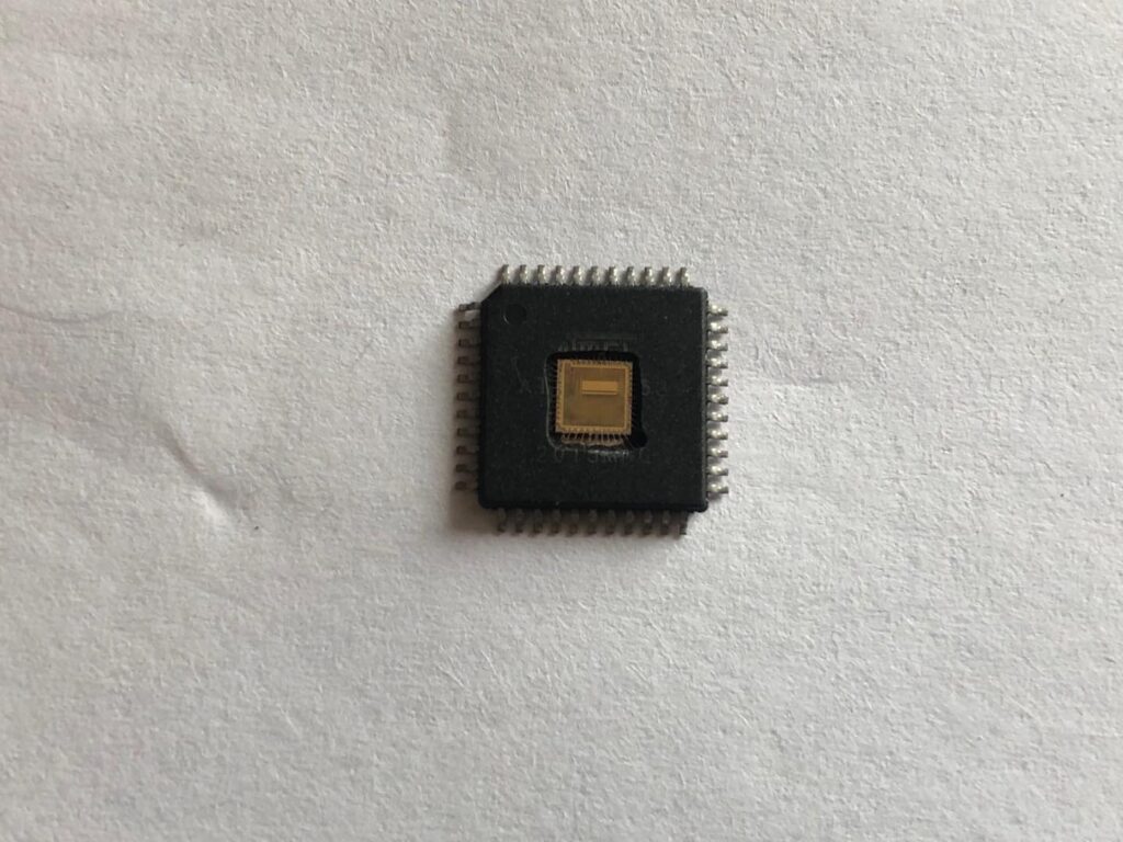
Reverse CPLD IC EPM7032AETI44-7 Eeprom JED File
Reverse CPLD IC EPM7032AETI44-7 Eeprom JED File starts from unlocking the security fuse bit of cpld epm7032aeti44 chip, the embedded jed file will be extracted from cpld chip;

Each LAB has 16 shareable expanders that can be viewed as a pool of uncommitted single product terms (one from each macrocell) with inverted outputs that feed back into the logic array.
El archivo JED de reprom CPLD IC EPM7032AETI44-7 inverso comienza al desbloquear el bit de fusible de seguridad del chip CPLD EPM7032AETI44, el archivo JED incrustado se extraerá del chip CPLD;
Each shareable expander can be used and shared by any or all macrocells in the LAB to build complex logic functions when reading cpld dump information. A small delay (tSEXP) is incurred when shareable expanders are used. Figure 3 shows how shareable expanders can feed multiple macrocells.
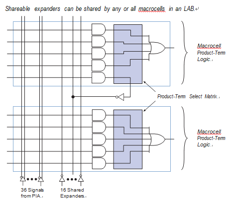
Parallel expanders are unused product terms that can be allocated to a neighboring macrocell to implement fast, complex logic functions.
Parallel expanders allow up to 20 product terms to directly feed the macrocell OR logic, with five product terms provided by the macrocell and 15 parallel expanders provided by neighboring macrocells in the LAB.
The compiler can allocate up to three sets of up to five parallel expanders to the macrocells that require additional product terms when attacking cpld encrypted code. Each set of five parallel expanders incurs a small, incremental timing delay (tPEXP).
reverzní CPLD IC EPM7032AETI44-7 reprom JED soubor začíná odemknutím bezpečnostního pojistkového bitu čipu cpld epm7032aeti44, vložený soubor jed bude extrahován z čipu cpld;
For example, if a macrocell requires 14 product terms, the compiler uses the five dedicated product terms within the macrocell and allocates two sets of parallel expanders; the first set includes five product terms, and the second set includes four product terms, increasing the total delay by 2 ´ tPEXP.
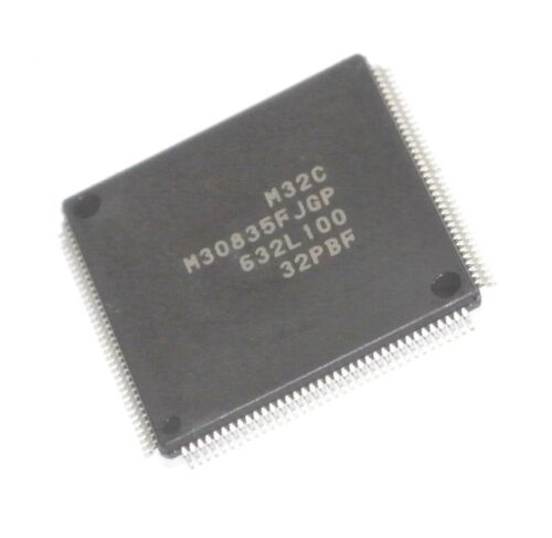
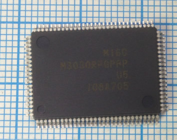
Renesas Microcontroller M30835FJGP Flash Memory Binary Cloning
Renesas Microcontroller M30835FJGP Flash Memory Binary Cloning is a process to discover embedded firmware from mcu M30835FJGP and readout source code from processor;
The M32C/83 Group (M32C/83, M32C/83T) microcomputer is a single-chip control unit that utilizes high performance silicon gate CMOS technology with the M32C/80 Series CPU core.
The M32C/83 Group (M32C/83, M32C/83T) is available in 144-pin and 100-pin plastic molded LQFP/QFP packages. With a 16-Mbyte address space, this microcomputer combines advanced instruction manipulation capabilities to process complex instructions by less bytes and execute instructions at higher speed when copying renesas m306nkfh microcontroller flash memory program.
La clonazione binaria del microcontrollore M30835FJGP della memoria flash Renesas è un processo per scoprire il firmware incorporato dall’MCU M30835FJGP e leggere il codice sorgente dal processore;
It includes a multiplier and DMAC adequate for office automation, communication devices and industrial equipments, and other high-speed processing applications.
| Characteristic | Performance | ||
| M32C/83 | M32C/83T | ||
| Basic Instructions | 108 instructions | ||
| Minimum Instruction Execution Time | 31.3 ns (f(BCLK) = 32 MHz, VCC = 4.2 to 5.5 V)50 ns (f(BCLK) = 20 MHz, VCC = 3.0 to 5.5 V) | 31.3 ns (f(BCLK) = 32 MHz, VCC=4.2 to 5.5 V) | |
| Operating Mode | Single-chip mode, Memory expansionmode and Microprocessor mode | Single-chip mode | |
| Address Space | 16 Mbytes | ||
| Memory Capacity | See Table 1.3 | ||
| I/O Port | 87 I/O pins and 1 input pin | ||
| Multifunction Timer | Timer A: 16 bits x 5 channels, Timer B: 16 bits x 6 channelsThree-phase motor control circuit | ||
| Intelligent I/O | Time measurement function: 16 bits x 5 channelsWaveform generating function: 16 bits x 10 channelsCommunication function (Clock synchronous serial I/O, Clock asynchronous se-rial I/O, HDLC data processing, Clock synchronous variable length serial I/O,(1)IEBus ) | ||
| Serial I/O | 5 Channels(1) 2 (2)Clock synchronous serial I/O, Clock asynchronous serial I/O, IEBus , I C bus | ||
| CAN Module | 1 channel Supporting CAN 2.0B specification | ||
| A/D Converter | 10-bit A/D converter: 2 circuits, 26 channels | ||
| D/A Converter | 8 bits x 2 channels | ||
| DMAC | 4 channels | ||
| DMAC II | Can be activated by all peripheral function interrupt sourcesImmediate transfer, Calculation transfer and Chain transfer functions | ||
| CRC Calculation Circuit | CRC-CCITT | ||
| X/Y Converter | 16 bits x 16 bits | ||
| Watchdog Timer | 15 bits x 1 channel (with prescaler) | ||
| Interrupt | 42 internal and 8 external sources, 5 software sourcesInterrupt priority level: 7 |
Copy Renesas Microcontroller M306NKFHGP#U3 Flash Program
Copy Renesas Microcontroller M306NKFHGP#U3 Flash Program needs to disable the protection over MCU M306NKFHGP#U3 by hacking technology and then extract IC chip code from embedded flash memory;
The M16C/6N Group (M16C/6N4) of MCUs are built using the high-performance silicon gate CMOS process using the M16C/60 Series CPU core and are packaged in 100-pin plastic molded QFP and LQFP.
These MCUs operate using sophisticated instructions featuring a high level of instruction efficiency. With 1 Mbyte of address space, they are capable of executing instructions at high speed when attacking renesas microcontroller r5f51115adfm3 flash memory. Being equipped with two CAN (Controller Area Network) modules in the M16C/6N Group (M16C/6N4), the MCU is suited to drive automotive and industrial control systems.
रेनेसास माइक्रोकंट्रोलर M306NKFHGP # यू 3 फ्लैश प्रोग्राम को हैकिंग तकनीक द्वारा एमसीयू M306NKFHGP # यू 3 पर सुरक्षा को अक्षम करने और फिर एम्बेडेड फ्लैश मेमोरी से आईसी चिप कोड निकालने की आवश्यकता है।
The CAN modules comply with the 2.0B specification. In addition, this MCU contains a multiplier and DMAC which combined with fast instruction processing capability, makes it suitable for control of various OA, communication, and industrial equipment which requires high-speed arithmetic/ logic operations.
1.1 Applications
· Automotive, industrial control systems and other automobile, other (T/V-ver. product)
· Car audio and industrial control systems, other (Normal-ver. product)
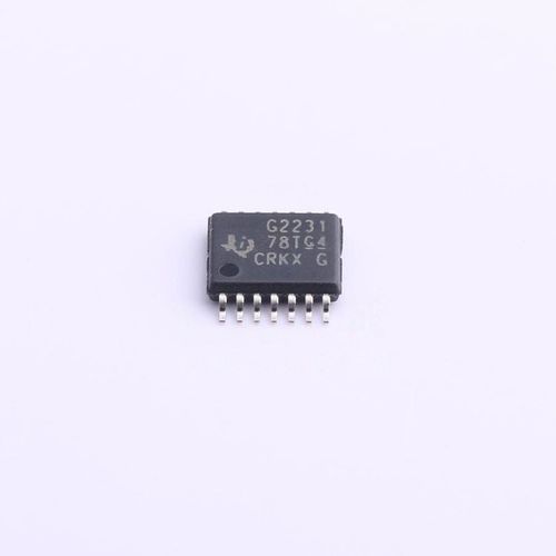
Mixed Signal CPU MSP430G2231 Secured Flash Program Replicating
Mixed Signal CPU MSP430G2231 Secured Flash Program Replicating will refer to extract locked code in the format of heximal from texas instrument microprocessor msp430g2231 after unlock microcontroller msp430g2231 flash memory;
The clock system is supported by the basic clock module that includes support for a 32768-Hz watch crystal oscillator, an internal very-low-power low-frequency oscillator, an internal digitally-controlled oscillator (DCO), and a high-frequency crystal oscillator.
The basic clock module is designed to meet the requirements of both low system cost and low power consumption to reverse microcontroller msp430g2112 flash memory. The internal DCO provides a fast turn- on clock source and stabilizes in less than 1 µs. The basic clock module provides the following clock signals:
मिश्रित सिग्नल सीपीयू MSP430G2231 सुरक्षित फ्लैश प्रोग्राम प्रतिकृति माइक्रोकंट्रोलर एमएसपी 430 जी 2231 फ्लैश मेमोरी को अनलॉक करने के बाद टेक्सास इंस्ट्रूमेंट माइक्रोप्रोसेसर एमएसपी 430 जी 2231 से समीपस्थ के प्रारूप में लॉक कोड निकालने का उल्लेख करेगा;
Auxiliary clock (ACLK), sourced from a 32768-Hz watch crystal, a high-frequency crystal, or the internal very-low-power LF oscillator.
Main clock (MCLK), the system clock used by the CPU.
Sub-Main clock (SMCLK), the sub-system clock used by the peripheral modules. The brownout circuit is implemented to provide the proper internal reset signal to the device during power on and power off which can be used for restoring msp430g2001 microcontroller heximal program.
There are four 8-bit I/O ports implemented—ports P1, P2, P3, and P4:
All individual I/O bits are independently programmable.
Any combination of input, output, and interrupt condition is possible.
Edge-selectable interrupt input capability for all eight bits of port P1 and P2.
Read and write access to port-control registers is supported by all instructions. Each I/O has an individually programmable pullup or pulldown resistor.
Recover Embedded Microprocessor MSP430G2131 Flash Software
Recover Embedded Microprocessor MSP430G2131 Flash Software is extract the locked firmware from mcu msp430g2131 flash memory after crack texas instrument msp430g2131 flash memory fuse bit;
The MSP430 bootstrap loader (BSL) enables users to program the flash memory or RAM using a UART serial interface. Access to the MSP430 memory via the BSL is protected by user-defined password which can provide convenience for breaking msp430g2452 microcontroller flash memory. For complete description of the features of the BSL and its implementation, see the MSP430 Programming Via the Bootstrap Loader User’s Guide.
फ्लैश सॉफ्टवेयर MSP430G2131 एम्बेडेड माइक्रोप्रोसेसर पुनर्प्राप्त करें टेक्सास उपकरण एमएसपी 430 जी 2131 फ्लैश मेमोरी फ्यूज बिट को क्रैक करने के बाद एमसीयू एमएसपी 430 जी 2131 फ्लैश मेमोरी से लॉक किए गए फर्मवेयर को निकालता है;
The flash memory can be programmed via the JTAG port, the bootstrap loader, or in-system by the CPU. The CPU can perform single-byte and single-word writes to the flash memory. Features of the flash memory include:
- Flash memory has n segments of main memory and four segments of information memory (A to D) of 64 bytes each. Each segment in main memory is 512 bytes in size.
- Segments 0 to n may be erased in one step, or each segment may be individually erased.
- Segments A to D can be erased individually, or as a group with segments 0 to n. Segments A to D are also called information memory.
Segment A contains calibration data. After reset, segment A is protected against programming and erasing by attacking ti mcu cpu msp430g2544 flash memory. It can be unlocked, but care should be taken not to erase this segment if the device-specific calibration data is required.
Texas Instrument MSP430G2121 Processor’s CPU memory Reverse Engineering
Texas Instrument MSP430G2121 Processor’s CPU memory Reverse Engineering is a process to unlock msp430g2121 microcontroller flash memory and readout embedded firmware from microcontroller;
To improve EMI on the XT1 oscillator the following guidelines should be observed:
Keep the trace between the device and the crystal as short as possible.
Design a good ground plane around the oscillator pins.
Das Reverse Engineering des CPU-Speichers des Texas Instrument MSP430G2121-Prozessors ist ein Prozess zum Entsperren des MSP430G2121-Mikrocontroller-Flash-Speichers und zum Auslesen der eingebetteten Firmware vom Mikrocontroller.
Prevent crosstalk from other clock or data lines into oscillator pins XIN and XOUT to replicate mcu msp430g2152 flash memory data.
Avoid running PCB traces underneath or adjacent to the XIN and XOUT pins.
Use assembly materials and processes that avoid any parasitic load on the oscillator XIN and XOUT pins.
If conformal coating is used, make sure that it does not induce capacitive or resistive leakage between the oscillator pins.
Do not route the XOUT line to the JTAG header to support the serial programming adapter as shown in other documentation. This signal is no longer required for the serial programming adapter.
Includes parasitic bond and package capacitance (approximately 2 pF per pin). Because the PCB adds additional capacitance, it is recommended to verify the correct load by measuring the ACLK frequency. For a correct setup, the effective load capacitance should always match the specification of the used crystal by attacking msp430g2312 microcontroller protective flash memory.
Requires external capacitors at both terminals. Values are specified by crystal manufacturers.
Frequencies below the MIN specification set the fault flag. Frequencies above the MAX specification do not set the fault flag. Frequencies between the MIN and MAX specifications might set the flag.
Measured with logic-level input frequency, but also applies to operation with crystals.
Reverse Engineering Texas Instrument Microcontroller MSP430G2444
Reverse Engineering Texas Instrument Microcontroller MSP430G2444 structure and locate the security fuse bit of MCU, unlock the protection over msp430g2444 flash memory and then extract TI MSP430G2444 flash program out from its memory;
To improve EMI on the XT1 oscillator, the following guidelines should be observed.
Keep the trace between the device and the crystal as short as possible.
Design a good ground plane around the oscillator pins to attack mcu msp430g2452 cpu flash memory protection.
Prevent crosstalk from other clock or data lines into oscillator pins XIN and XOUT.
Avoid running PCB traces underneath or adjacent to the XIN and XOUT pins.
Reverse Engineering des Mikrocontrollers von Texas Instrument MSP430G2444 das Sicherheitssicherungsbit der MCU strukturieren und lokalisieren, den Schutz über den MSP430G2444-Flash-Speicher entsperren und dann das TI-MSP430G2444-Flash-Programm aus dem Speicher extrahieren.
Use assembly materials and processes that avoid any parasitic load on the oscillator XIN and XOUT pins.
If conformal coating is used, make sure that it does not induce capacitive or resistive leakage between the oscillator pins.
Do not route the XOUT line to the JTAG header to support the serial programming adapter as shown in other documentation. This signal is no longer required for the serial programming adapter when restoring mcu msp430g2452 flash memory binary.
Includes parasitic bond and package capacitance (approximately 2 pF per pin).
Because the PCB adds additional capacitance, it is recommended to verify the correct load by measuring the ACLK frequency. For a correct setup, the effective load capacitance should always match the specification of the crystal that is used.
Frequencies below the MIN specification set the fault flag. Frequencies above the MAX specification do not set the fault flag. Frequencies between the MIN and MAX specifications might set the flag.
Measured with logic-level input frequency but also applies to operation with crystals.