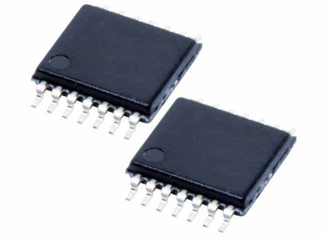
 Texas Instrument MSP430G2513 CPU Processor Flash Unlocking
Texas Instrument MSP430G2513 CPU Processor Flash Unlocking refers to attack msp430g2513 secured flash memory by focus ion beam and then extract ti microprocessor msp430g2513 locked code from flash memory;
- To improve EMI on the XT1 oscillator, the following guidelines should be observed.
- Keep the trace between the device and the crystal as short as possible.
- Design a good ground plane around the oscillator pins.
- Prevent crosstalk from other clock or data lines into oscillator pins XIN and XOUT.
- Avoid running PCB traces underneath or adjacent to the XIN and XOUT pins.
- Use assembly materials and process that avoid any parasitic load on the oscillator XIN and XOUT pins.
- If a conformal coating is used, ensure that it does not induce capacitive or resistive leakage between the oscillator pins.
- Do not route the XOUT line to the JTAG header to support the serial programming adapter as shown in other documentation. This signal is no longer required for the serial programming adapter.
- Includes parasitic bond and package capacitance when replicating texas instrument msp430g2152 flash memory data (approximately 2 pF per pin).
Because the PCB adds additional capacitance, it is recommended to verify the correct load by measuring the ACLK frequency. For a correct setup, the effective load capacitance should always match the specification of the used crystal when break msp430g2412 locked flash memory.
Texas Instrument MSP430G2513 CPU processore flash sblocco si riferisce all’attacco msp430g2513 protetto memoria flash da focus ion beam e quindi estrarre il codice bloccato del microprocessore ti msp430g2513 dalla memoria flash;
- Frequencies below the MIN specification set the fault flag. Frequencies above the MAX specification do not set the fault flag. Frequencies in between might set the flag.
- Measured with logic-level input frequency but also applies to operation with crystals.
Texas Instrument MSP430G2413 Microcontroller Flash Cracking
Texas Instrument MSP430G2413 Microcontroller Flash Cracking will need engineer to unlock encrypted mcu msp430g2413 protective fuse bit and readout flash program from mixed signal MCU directly;
Universal Serial Communications Interface (USCI)
The USCI module is used for serial data communication. The USCI module supports synchronous communication protocols such as SPI (3 or 4 pin) and I2C, and asynchronous communication protocols such as UART, enhanced UART with automatic baudrate detection (LIN), and IrDA. Not all packages support the USCI functionality when recover microcontroller msp430g2131 flash software program.
Texas Instrument MSP430G2413 microcontroller flash cracking avrà bisogno di ingegnere per sbloccare MCU crittografato MSP430G2413 bit fusibile protettivo e programma flash di lettura direttamente dall’MCU a segnale misto;
USCI_A0 provides support for SPI (3 or 4 pin), UART, enhanced UART, and IrDA. USCI_B0 provides support for SPI (3 or 4 pin) and I2C.
Comparator_A+
The primary function of the comparator_A+ module is to support precision slope analog-to-digital conversions, battery-voltage supervision, and monitoring of external analog signals.
ADC10 (MSP430G2x53 Only)
The ADC10 module supports fast 10-bit analog-to-digital conversions. The module implements a 10-bit SAR core, sample select control, reference generator, and data transfer controller (DTC) for automatic conversion result handling, allowing ADC samples to be converted and stored without any CPU intervention after break msp430g2452 locked microcontroller flash memory.
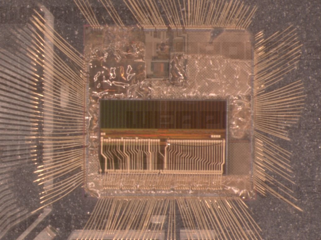
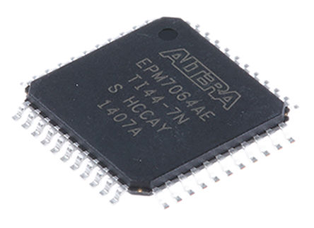
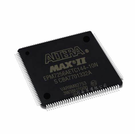
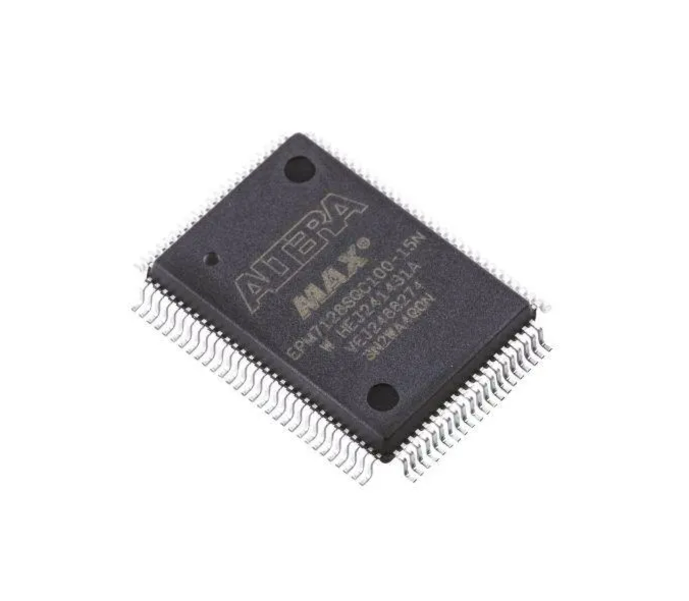
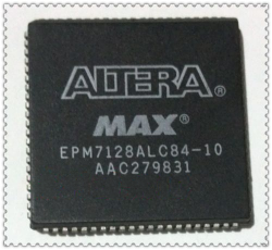
Altera CPLD EPM7256ATC144 Chip Eeprom Data Decoding
Altera CPLD EPM7256ATC144 Chip Eeprom Data Decoding needs to crack altera pld epm7256atc protective system and reset the status of CPLD IC from locked to unlock, extract embedded software from IC CPLD chip;
- See the Operating Requirements for Altera Devices Data Sheet.
- Minimum DC input voltage is –0.5 V. During transitions, the inputs may undershoot to –2.0 V for input currents less than 100 mA and periods shorter than 20 ns.
- For EPM7128A and EPM7256A devices only, VCC must rise monotonically.
- In MAX 7000AE devices, all pins, including dedicated inputs, I/O pins, and JTAG pins, may be driven before VCCINT and VCCIO are powered.
- These devices support in-system programming for –40° to 100° C. For in-system programming support between –40° and 0° C, contact Altera Applications.
These values are specified under the recommended operating conditions shown in Table 14 on page 28.
Le décodage de données de la puce Altera CPLD EPM7256ATC144 doit déchiffrer le système de protection Altera PLD EPM7256ATC et réinitialiser l’état de CPLD IC de verrouillé à déverrouiller, extraire le logiciel embarqué de la puce IC CPLD;
The parameter is measured with 50% of the outputs each sourcing the specified current. The IOH parameter refers to high-level TTL or CMOS output current for the purpose of recovering altera cpld epm7128alc eeprom program.
The parameter is measured with 50% of the outputs each sinking the specified current. The IOL parameter refers to low-level TTL or CMOS output current.
This value is specified for normal device operation. For MAX 7000AE devices, the maximum leakage current during power-up is ±300 mA. For EPM7128A and EPM7256A devices, leakage current during power-up is not specified which is especially useful features for recover cpld epm7032vtc system memory content.
(10) For EPM7128A and EPM7256A devices, this pull-up exists while a device is programmed in-system.
For MAX 7000AE devices, this pull-up exists while devices are programmed in-system and in unprogrammed devices during power-up.
Capacitance is measured at 25 °C and is sample-tested only. The OE1 pin (high-voltage pin during programming) has a maximum capacitance of 20 pF.
The POR time for MAX 7000AE devices (except MAX 7128A and MAX 7256A devices) does not exceed 100 ms. The sufficient VCCINT voltage level for POR is 3.0 V. The device is fully initialized within the POR time after VCCINT reaches the sufficient POR voltage level.
Attack Altera PLD EPM7256BTI144 Secured Eeprom
Attack Altera PLD EPM7256BTI144 Secured Eeprom and copy PLD jed file out from original eeprom memory area, the status of master altera pld epm7256bit unit will be decrypted;
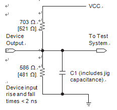
Power supply transients can affect AC measurements. Simultaneous transitions of multiple outputs should be avoided for accurate measurement. Threshold tests must not be performed under AC conditions.
Large-amplitude, fast-ground- current transients normally occur as the device outputs discharge the load capacitances in order to attack epm7064stc eeprom memory. When these transients flow through the parasitic inductance between the device ground pin and the test system ground, significant reductions in observable noise immunity can result.
attaque Altera PLD EPM7256BTI144 eeprom sécurisé et copie PLD jed fichier hors de la zone de mémoire eeprom d’origine, le statut de l’unité maître Altera PLD EPM7256bit sera décrypté;
Numbers in brackets are for 2.5-V outputs. Numbers without brackets are for 3.3-V outputs.
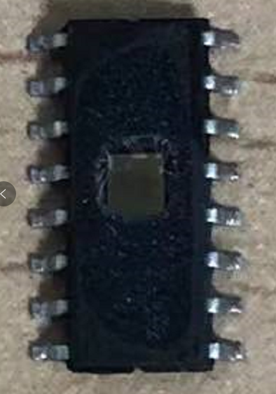
Texas Instruments MSP430G2313 Microprocessor Breaking
Texas Instruments MSP430G2313 Microprocessor Breaking refers to unlock the protection over msp430g2313 flash memory and eeprom memory, and then extract embedded code from mcu msp430g2313;
JTAG FUSE
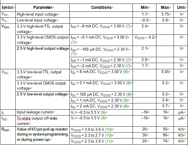
over recommended ranges of supply voltage and operating free-air temperature (unless otherwise noted)
| PARAMETER | TEST CONDITIONS | MIN | MAX | UNIT | |
| VCC(FB) | Supply voltage during fuse-blow condition | TA = 25°C | 2.5 | V | |
| VFB | Voltage level on TEST for fuse blow | 6 | 7 | V | |
| IFB | Supply current into TEST during fuse blow | 100 | mA | ||
| tFB | Time to blow fuse | 1 | ms |
(1) Once the fuse is blown, no further access to the JTAG/Test, Spy-Bi-Wire, and emulation feature is possible, and JTAG is switched to bypass mode.
Calibration data is stored for both the DCO and for ADC10 organized in a tag-length-value structure by replicate msp430g2152 flash memory data.
La rupture du microprocesseur MSP430G2313 de Texas Instruments consiste à déverrouiller la protection sur la mémoire flash MSP430G2313 et la mémoire EEPROM, puis à extraire le code intégré du MCU MSP430G2313;
Table 10. Tags Used by the ADC Calibration Tags
| NAME | ADDRESS | VALUE | DESCRIPTION |
| TAG_DCO_30 | 0x10F6 | 0x01 | DCO frequency calibration at VCC = 3 V and TA = 30°C at calibration |
| TAG_ADC10_1 | 0x10DA | 0x10 | ADC10_1 calibration tag |
| TAG_EMPTY | – | 0xFE | Identifier for empty memory areas |
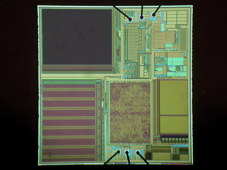
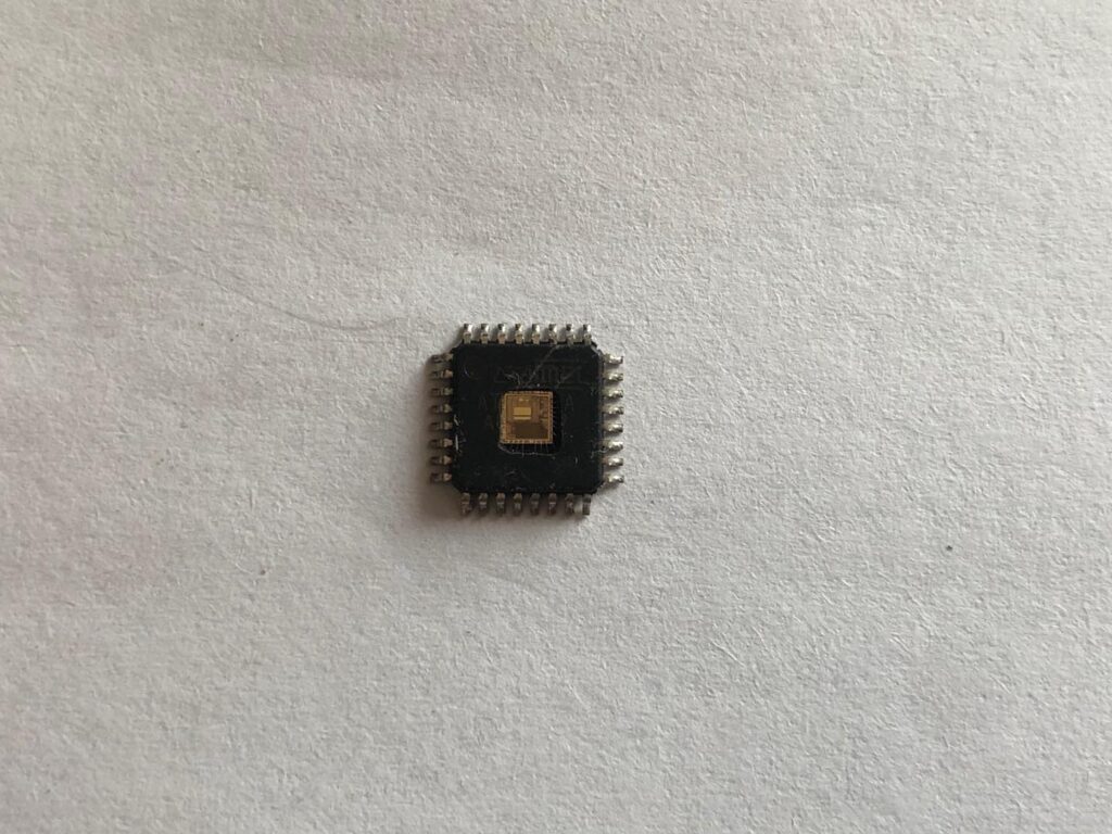
Texas Instruments MSP430G2213 Microcontroller Memory Reverse Engineering
Texas Instruments MSP430G2213 Microcontroller Memory Reverse Engineering technique will help to locate the security fuse bit of mcu msp430g2213 and crack it by focus ion beam, and then extract embedded heximal program out from msp430g2213 mcu;
RAM

Texas Instruments MSP430G2213 técnica de engenharia reversa de memória microcontrolador ajudará a localizar o bit de fusível de segurança do mcu msp430g2213 e quebrá-lo por feixe de íons de foco e, em seguida, extrair o programa heximal incorporado do msp430g2213 mcu
over recommended ranges of supply voltage and operating free-air temperature (unless otherwise noted)
| PARAMETER | TEST CONDITIONS | MIN MAX | UNIT |
| V(RAMh) RAM retention supply voltage (1) | CPU halted | 1.6 | V |
(1) This parameter defines the minimum supply voltage VCC when the data in RAM remains unchanged which can be used for restoring msp430g2001 heximal program. No program execution should happen during this supply voltage condition.
JTAG and Spy-Bi-Wire Interface
over recommended ranges of supply voltage and operating free-air temperature (unless otherwise noted)
| PARAMETER | TEST CONDITIONS | VCC | MIN | TYP | MAX | UNIT | ||
| fSBW | Spy-Bi-Wire input frequency | 2.2 V | 0 | 20 | MHz | |||
| tSBW,Low | Spy-Bi-Wire low clock pulse duration | 2.2 V | 0.025 15 | µs | ||||
| tSBW,En | Spy-Bi-Wire enable time (TEST high to acceptance of first clock edge | (1)) | 2.2 V | 1 | µs | |||
| tSBW,Ret | Spy-Bi-Wire return to normal operation time | 2.2 V | 15 | 100 | µs | |||
| fTCK | TCK input frequency(2) | 2.2 V | 0 | 5 | MHz | |||
| RInternal | Internal pulldown resistance on TEST | 2.2 V | 25 | 60 | 90 | kΩ |
Altera Programmable Logic Device EPM7128BUC169 Firmware Restoration
Altera Programmable Logic Device EPM7128BUC169 Firmware Restoration means the embedded eeprom memory inside original PLD EPM7128BUC processor will be unlocked and firmware can be fully extracted from IC CPLD;
All MAX 7000A devices contain a programmable security bit that controls access to the data programmed into the device. When this bit is programmed, a design implemented in the device cannot be copied or retrieved.
This feature provides a high level of design security because programmed data within EEPROM cells is invisible. The security bit that controls this function, as well as all other programmed data, is reset only when the device is reprogrammed after reverse engineering cpld epm7032aeti44 memory.
Le dispositif logique programmable Altera EPM7128BUC169 la restauration du firmware signifient que la mémoire eeprom intégrée à l’intérieur du processeur PLD EPM7128BUC d’origine sera déverrouillée et que le firmware pourra être entièrement extrait de IC CPLD
MAX 7000A devices are fully tested. Complete testing of each
programmable EEPROM bit and all internal logic elements ensures 100% programming yield. AC test measurements are taken under conditions equivalent to those shown. Test patterns can be used and then erased during early stages of the production flow when recover cpld epm7128 embedded eeprom program.
Altera CPLD EPM7128ALC Embedded Eeprom Program Recovery
Altera CPLD EPM7128ALC Embedded Eeprom Program Recovery is a process to unlock security fuse bit of EPM7128 CPLD chip and extract eeprom firmware from CPLD’s secured memory in the format of JED;
Because MAX 7000A devices can be used in a mixed-voltage environment, they have been designed specifically to tolerate any possible power-up sequence. The VCCIO and VCCINT power planes can be powered in any order.
Signals can be driven into MAX 7000AE devices before and during power- up (and power-down) without damaging the device.
Additionally, MAX 7000AE devices do not drive out during power-up when breaking altera cpld epm7064aetc protection. Once operating conditions are reached, MAX 7000AE devices operate as specified by the user.
Altera CPLD EPM7128ALC recuperación del programa eeprom integrado es un proceso para desbloquear el bit de fusible de seguridad de EPM7128 chip CPLD y extraer el firmware eeprom de la memoria segura de CPLD en el formato de JED
MAX 7000AE device I/O pins will not source or sink more than 300 µA of DC current during power-up. All pins can be driven up to 5.75 V during hot-socketing, except the OE1 and GLCRn pins.
The OE1 and GLCRn pins can be driven up to 3.6 V during hot-socketing. After VCCINT and VCCIO reach the recommended operating conditions, these two pins are 5.0-V tolerant which can be used for recover embedded eeprom firmware of EPM7032VTC cpld chipset.
EPM7128A and EPM7256A devices do not support hot-socketing and may drive out during power-up.
Altera PLD EPM7128ALC84 IC Breaking
Altera PLD EPM7128ALC84 IC Breaking involve the unlocking of epm7128 eeprom memory tamper resistance system and extract embedded jed software from pld eeprom memory;
MAX 7000S devices
– ISP circuitry compatible with IEEE Std. 1532
Includes 5.0-V MAX 7000 devices and 5.0-V ISP-based MAX 7000S devices
Built-in JTAG boundary-scan test (BST) circuitry in MAX 7000S devices with 128 or more macrocells
Complete EPLD family with logic densities ranging from 600 to 5,000 usable gates (see Tables 1 and 2) 5-ns pin-to-pin logic delays with up to 175.4-MHz counter frequencies (including interconnect)
PCI-compliant devices available
Open-drain output option in MAX 7000S devices
La rottura del circuito integrato EPM7128ALC84 PLD Altera comporta lo sblocco del sistema di resistenza alla manomissione della memoria epm7128 eeprom e l’estrazione del software jed incorporato dalla memoria eeprom pld;
Programmable macrocell flipflops with individual clear, preset, clock, and clock enable controls
Programmable power-saving mode for a reduction of over 50% in each macrocell
Configurable expander product-term distribution, allowing up to 32 product terms per macrocell 44 to 208 pins available in plastic J-lead chip carrier (PLCC), ceramic pin-grid array (PGA), plastic quad flat pack (PQFP), power quad flat pack (RQFP), and 1.0-mm thin quad flat pack (TQFP) packages Programmable security bit for protection of proprietary designs 3.3-V or 5.0-V operation.
– MultiVoltTM I/O interface operation, allowing devices to interface with 3.3-V or 5.0-V devices (MultiVolt I/O operation is not available in 44-pin packages)
– Pin compatible with low-voltage MAX 7000A and MAX 7000B devices
Enhanced features available in MAX 7000E and MAX 7000S devices
– Six pin- or logic-driven output enable signals
– Two global clock signals with optional inversion
– Enhanced interconnect resources for improved routability
– Fast input setup times provided by a dedicated path from I/O pin to macrocell registers
– Programmable output slew-rate control
Software design support and automatic place-and-route provided by Altera’s development system for Windows-based PCs and Sun SPARCstation, and HP 9000 Series 700/800 workstations Additional design entry and simulation support provided by EDIF 2 0 0 and 3 0 0 netlist files, library of parameterized modules (LPM) when attacking cpld altera epm7064stc eeprom memory,
Verilog HDL, VHDL, and other interfaces to popular EDA tools from manufacturers such as Cadence, Exemplar Logic, Mentor Graphics, OrCAD, Synopsys, and VeriBest
Programming support
– Altera’s Master Programming Unit (MPU) and programming hardware from third-party manufacturers program all MAX 7000 devices
– The BitBlasterTM serial download cable, ByteBlasterMVTM parallel port download cable, and MasterBlasterTM serial/universal serial bus (USB) download cable program MAX 7000S devices
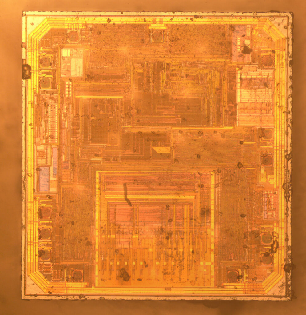
Attack Altera CPLD EPM7064STC44-10 IC Eeprom Memory
Attack Altera CPLD EPM7064STC44-10 IC Eeprom Memory needs to crack altera cpld epm7064 fuse bit and extract embedded jed file from eeprom memory;
MAX 7000A devices provide an optional open-drain (equivalent to open-collector) output for each I/O pin. This open-drain output enables the device to provide system-level control signals to recovering cpld epm7032vtc eeprom code (e.g., interrupt and write enable signals) that can be asserted by any of several devices. This output can also provide an additional wired-OR plane.
Open-drain output pins on MAX 7000A devices (with a pull-up resistor to the 5.0-V supply) can drive 5.0-V CMOS input pins that require a high VIH. When the open-drain pin is active, it will drive low. When the pin is inactive, the resistor will pull up the trace to 5.0 V to meet CMOS VOH requirements.
атака Altera CPLD EPM7064STC44-10 IC Пам’ять eeprom повинна зламати біт запобіжника Altera CPLD EPM7064 і витягти вбудований файл JED з пам’яті eeprom;
The open-drain pin will only drive low or tri-state; it will never drive high. The rise time is dependent on the value of the pull-up resistor and load impedance by reversing cpld epm7032aeti44 eeprom jed file. The IOL current specification should be considered when selecting a pull-up resistor.