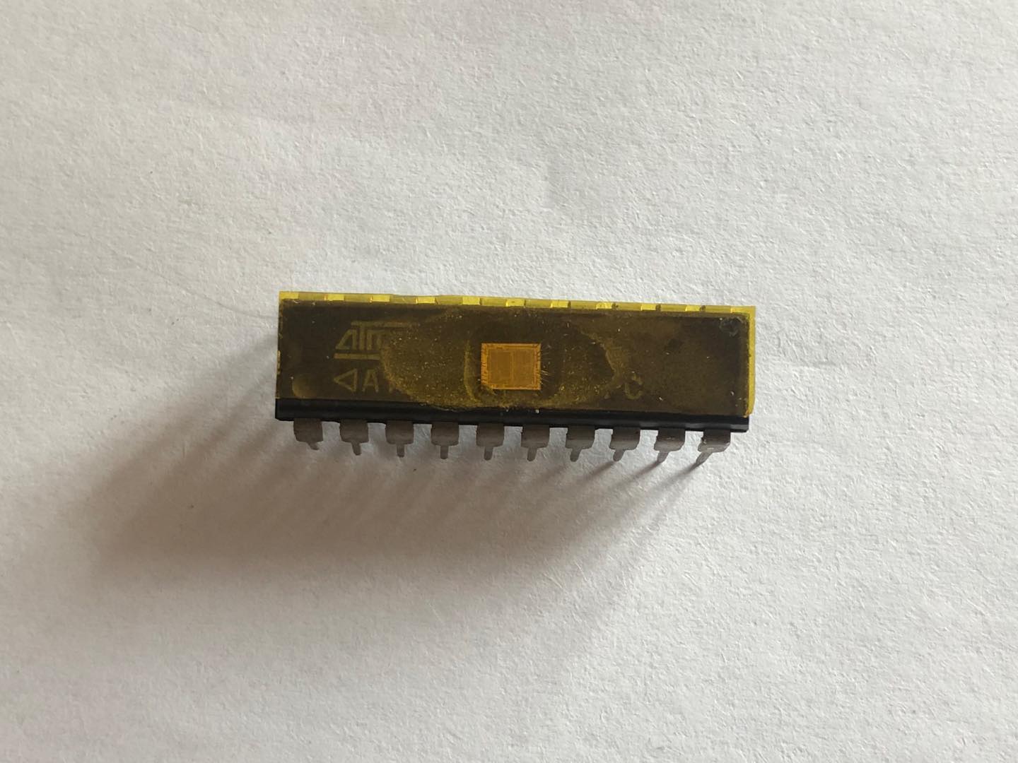
 ST72F325J6 Microcontroller Flash Memory Program Code Extraction
ST72F325J6 Microcontroller Flash Memory Program Code Extraction refers to crack mcu st72f325J6 tamper resistance system and then copy chip heximal file to new st72f325j6;
Notes:
- The contents of the I/O port DR registers are readable only in output configuration. In input configuration, the values of the I/O pins are returned instead of the DR register contents.
- The bits associated with unavailable pins must always keep their reset value.
- The Timer A Input Capture 2 pin is not available (not bonded).
- In Flash devices:
The TAIC2HR and TAIC2LR registers are not present. Bit 5 of the TACSR register (ICF2) is forced by hardware to 0. Consequently, the corresponding interrupt cannot be used when decrypting st72f321bk microprocessor flash memory program.
The Timer A Output Compare 2 pin is not available (not bonded).
The TAOC2HR and TAOC2LR Registers are write only, reading them will return undefined values. Bit 4 of the TACSR register (OCF2) is forced by hardware to 0. Consequently, the corresponding interrupt cannot be used.
Caution: The TAIC2HR and TAIC2LR registers and the ICF2 and OCF2 flags are not present in Flash de- vices but are present in the emulator. For compatibility with the emulator, it is recommended to perform a dummy access (read or write) to the TAIC2LR and TAOC2LR registers to clear the interrupt flags only after decoding st72f321r9 processor memory file.
Cracking 8 BIT ST72F324K4 Locked MCU Flash Program
Cracking 8 BIT ST72F324K4 Locked MCU Flash Program starts from remove silicon package over microprocessor and then readout embedded firmware from microcontroller’s flash memory, and copy original binary to new MCU;
In the interrupt input column, “eiX” defines the associated external interrupt vector. If the weak pull-up column (wpu) is merged with the interrupt column (int), then the I/O configuration is pull-up interrupt input, else the configuration is floating interrupt input.
In the open drain output column, “T” defines a true open drain I/O (P-Buffer and protection diode to VDD are not implemented). See See “I/O PORTS” on page 45. and Section 12.9 I/O PORT PIN CHARACTER- ISTICS for more details.
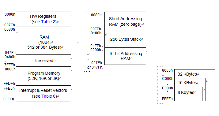
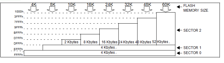
As shown in below Figure, the MCU is capable of ad- dressing 64K bytes of memories and I/O registers. The available memory locations consist of 128 bytes of register locations after , up to 1024 bytes of RAM and up to 32 Kbytes of user program memory. The RAM space includes up to 256 bytes for the stack from 0100h to 01FFh after cracking st72f321m9 microprocessor flash memory.
OSC1 and OSC2 pins connect a crystal/ceramic resonator, or an external source to the on-chip oscillator; see Section 1 INTRODUCTION and Section 12.6 CLOCK AND TIMING CHARACTERISTICS for more details.
On the chip, each I/O port has 8 pads. Pads that are not bonded to external pins are in input pull-up configuration after reset. The configuration of these pads must be kept at reset state to avoid added current consumption.
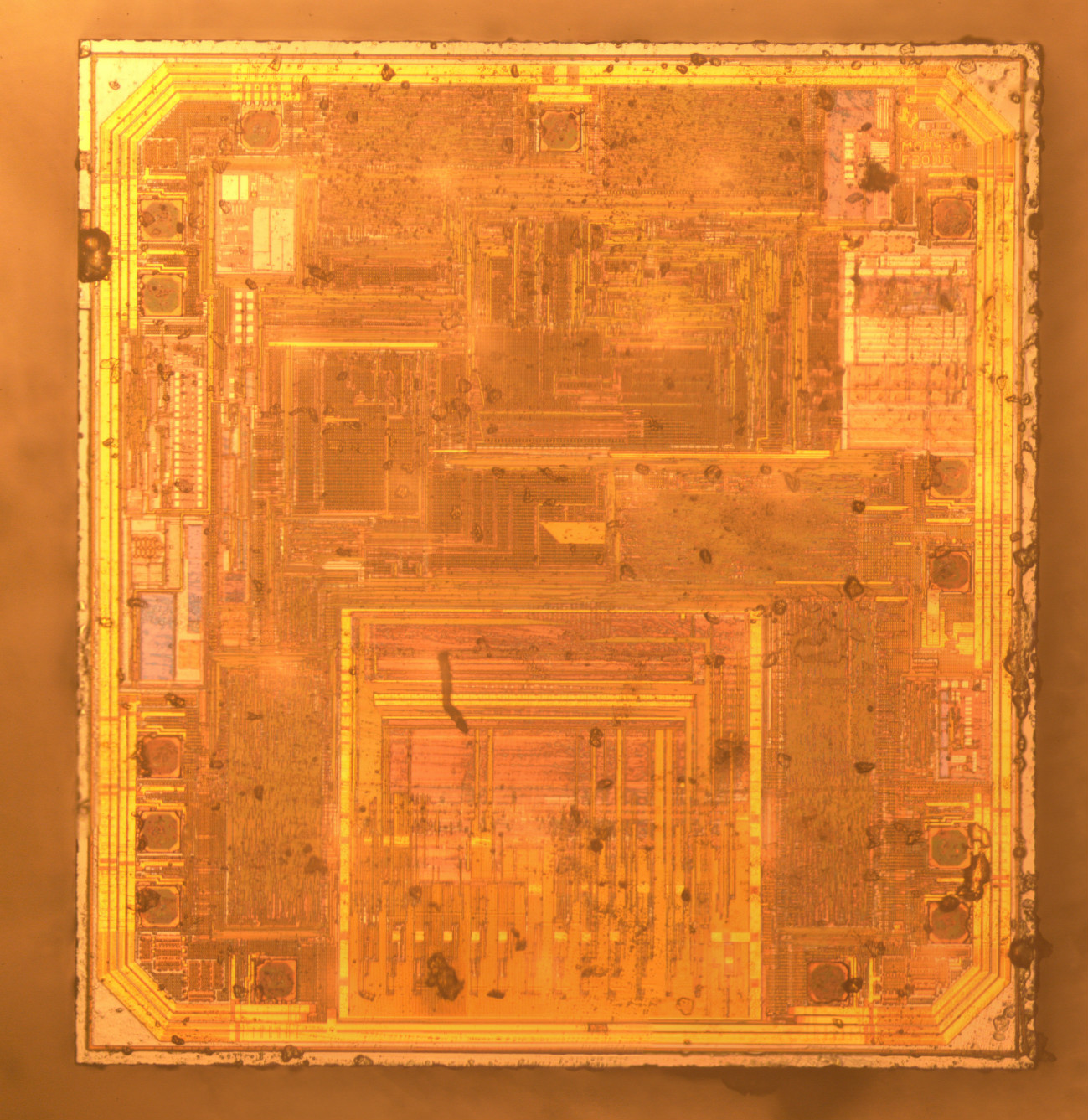
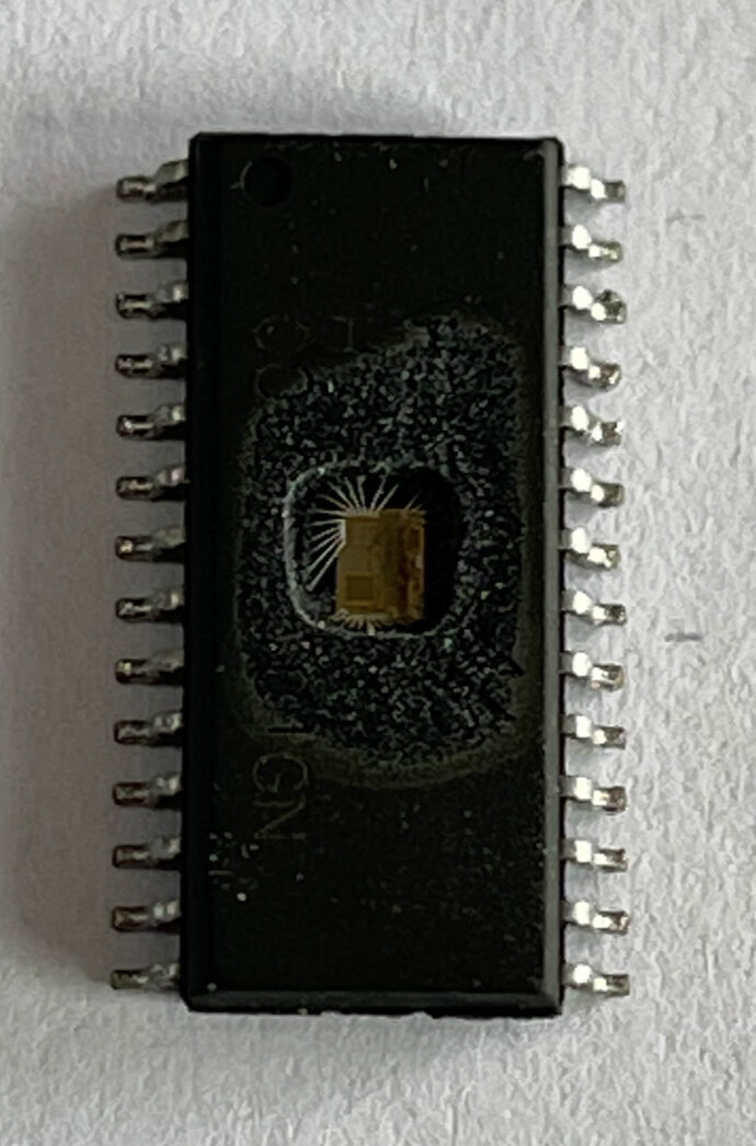
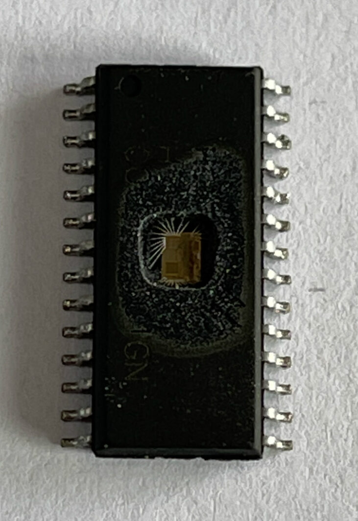
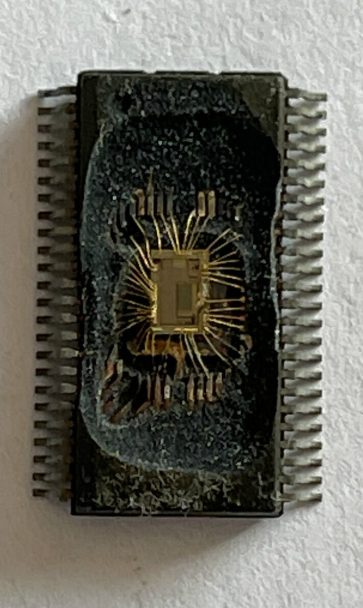
Reverse Engineering ST72F324BK MCU Heximal
Reverse Engineering ST72F324BK MCU Heximal is a process to cracking stm72f324bk microcontroller locked bits by focus ion beam, readout embedded firmware program from processor’s st72f324bk flash memory.
The ST72324 devices are members of the ST7 mi- crocontroller family designed for the 5V operating range.
The 32-pin devices are designed for mid-range applications
The 42/44-pin devices target the same range of applications requiring more than 24 I/O ports.
All devices are based on a common industry- standard 8-bit core, featuring an enhanced instruction set and are available with FLASH program memory.
Under software control, all devices can be placed in WAIT, SLOW, ACTIVE-HALT or HALT mode, reducing power consumption when the application is in idle or stand-by state.
The enhanced instruction set and addressing modes of the ST7 offer both power and flexibility to software developers, enabling the design of highly efficient and compact application code in the process of microcontroller st72f321ba flash memory source code extraction. In addition to standard 8-bit data management, all ST7 microcontrollers feature true bit manipulation, 8×8 un- signed multiplication and indirect addressing modes.
Crack ST32F324J6 Microcontroller Locked Bit
Crack ST32F324J6 Microcontroller Locked Bit can help to disable the protection over MCU ST32F324J6 and then recover embedded firmware from st32f324j6 flash memory, copy heximal file to new st32f324j6 for MCU cloning;
8 to 32K dual voltage High Density Flash (HD- Flash) with read-out protection capability. In- Application Programming and In-Circuit Pro- gramming for HD Flash devices.
384 to 1K bytes RAM
HD Flash endurance: 100 cycles, data reten- tion: 20 years at 55°C
Enhanced low voltage supervisor (LVD) for main supply with programmable reset thresh- olds and auxiliary voltage detector (AVD) with interrupt capability when breaking st72f321j9 mcu flash memory;
Clock sources: crystal/ceramic resonator os- cillators, internal RC oscillator, clock security system and bypass for external clock
PLL for 2x frequency multiplication
Four Power Saving Modes: Halt, Active-Halt, Wait and Slow
Nested interrupt controller
10 interrupt vectors plus TRAP and RESET
9/6 external interrupt lines (on 4 vectors)
ARM Locked MCU STM32F071VCT6 Protection Cracking
Through ARM Locked MCU STM32F071VCT6 Protection Cracking, embedded firmware from stm32f071 microcontroller flash memory can be recovered, and copy the firmware heximal file to new MCU stm32f071.
Several prescalers and PLLs allow the configuration of the three AHB buses, the high- speed APB (APB2) and the low-speed APB (APB1) domains. The maximum frequency of the three AHB buses is 120 MHz and the maximum frequency the high-speed APB domains is 60 MHz.
The maximum allowed frequency of the low-speed APB domain is 30 MHz. The devices embed a dedicate PLL (PLLI2S) that allow them to achieve audio class performance by restoring arm microcontroller stm32f103 flash memory file. In this case, the I2S master clock can generate all standard sampling frequencies from 8 kHz to 192 kHz.
At startup, boot pins are used to select one out of three boot options:
Boot from user Flash memory
Boot from system memory
Boot from embedded SRAM
The boot loader is located in system memory. It is used to reprogram the Flash memory by using USART1 (PA9/PA10), USART3 (PC10/PC11 or PB10/PB11), CAN2 (PB5/PB13), USB OTG FS in Device mode (PA11/PA12) through DFU after recovering stm32f103c6 flash memory full content (device firmware upgrade).
Unlock ARM Microcontroller STM32F070RCT6 Secured Flash Memory
Unlock ARM Microcontroller STM32F070RCT6 Secured Flash Memory needs to use focus ion beam to disable its fuse bit, extract arm microprocessor stm32f070 flash memory data and clone the heximal to new stm32f070 MCU;
External interrupt/event controller (EXTI)
The external interrupt/event controller consists of 23 edge-detector lines used to generate interrupt/event requests. Each line can be independently configured to select the trigger event (rising edge, falling edge, both) and can be masked independently in order to replicate arm mcu stm32f105 embedded flash firmware. A pending register maintains the status of the interrupt requests. The EXTI can detect an external line with a pulse width shorter than the Internal APB2 clock period. Up to 140 GPIOs can be connected to the 16 external interrupt lines.
Clocks and startup
On reset the 16 MHz internal RC oscillator is selected as the default CPU clock. The 16 MHz internal RC oscillator is factory-trimmed to offer 1% accuracy. The application can then select as system clock either the RC oscillator or an external 4-26 MHz clock source.
This clock is monitored for failure. If failure is detected, the system automatically switches back to the internal RC oscillator and a software interrupt is generated (if enabled) after decrypt arm mcu stm32f105 flash memory binary file. Similarly, full interrupt management of the PLL clock entry is available when necessary (for example if an indirectly used external oscillator fails).
The advanced clock controller clocks the core and all peripherals using a single crystal or oscillator. In particular, the ethernet and USB OTG FS peripherals can be clocked by the system clock.
Microprocessor ST72F324BJ Program Flash Memory Unlocking
Microprocessor ST72F324BJ Program Flash Memory Unlocking will take the advantage of focus ion beam to remove the fuse bit embedded and pull embedded firmware out from mcu st72f324bj memory, after a few moment later these extracted heximal can be copied to new st72f324bj for micrcontroller cloning;
The ST7 dual voltage High Density Flash (HDFlash) is a non-volatile memory that can be electrically erased as a single block or by individu- al sectors and programmed on a Byte-by-Byte ba- sis using an external VPP supply.
The HDFlash devices can be programmed and erased off-board (plugged in a programming tool) or on-board using ICP (In-Circuit Programming) or IAP (In-Application Programming). The array matrix organisation allows each sector to be erased and reprogrammed without affecting other sectors.
Read-out protection, when selected, provides a protection against Program Memory content ex- traction and against write access to Flash memo- ry. Even if no protection can be considered as to- tally unbreakable, the feature provides a very high level of protection for a general purpose microcon- troller.
In flash devices, this protection is removed by re- programming the option. In this case, the entire program memory is first automatically erased and the device can be reprogrammed.
Read-out protection selection depends on the de- vice type:
- In Flash devices it is enabled and removed through the FMP_R bit in the option byte.
In ROM devices it is enabled by mask option specified in the Option List.
Crack ST72F321M9 Secured Microcontroller
Crack ST72F321M9 Secured Microcontroller and pull the embedded firmware from st72f321m9 locked flash memory, copy heximal file into new microprocessor st72f321m9 memory;
the MCU is capable of addressing 64K bytes of memories and I/O registers. The available memory locations consist of 128 bytes of register locations, up to 2Kbytes of RAM and up to 60Kbytes of user program memory when st72f321bk mcu flash memory program decryption. The RAM space includes up to 256 bytes for the stack from 0100h to 01FFh.
The highest address bytes contain the user reset and interrupt vectors.
IMPORTANT: Memory locations marked as “Re- served” must never be accessed. Accessing a re- seved area can have unpredictable effects on the device.
Related Documentation
AN 985: Executing Code in ST7 RAM
The ST7 dual voltage High Density Flash (HDFlash) is a non-volatile memory that can be electrically erased as a single block or by individu- al sectors and programmed on a Byte-by-Byte ba- sis using an external VPP supply.
The HDFlash devices can be programmed and erased off-board (plugged in a programming tool) or on-board using ICP (In-Circuit Programming) or IAP (In-Application Programming) even in the process of decoding mcu st72f321r9 locked memory file. The array matrix organisation allows each sector to be erased and reprogrammed without affecting other sectors.
Extract Microcontroller ST72F321BAR9T6 Flash Memory Source Code
Extract Microcontroller ST72F321BAR9T6 Flash Memory Source Code needs to use focus ion beam to remove its security fuse bit which will refers to pull embedded firmware from st72f321ba flash memory, and then copy flash firmware in the format of heximal to new st72f321ba mcu chip;
The ST7 dual voltage High Density Flash (HDFlash) is a non-volatile memory that can be electrically erased as a single block or by individu- al sectors and programmed on a Byte-by-Byte ba- sis using an external VPP supply.
The HDFlash devices can be programmed and erased off-board (plugged in a programming tool) or on-board using ICP (In-Circuit Programming) or IAP (In-Application Programming). The array matrix organisation allows each sector to be erased and reprogrammed without affecting other sectors when breaking st72f321ar ic chip memory protection.
Three Flash programming modes:
Insertion in a programming tool. In this mode, all sectors including option bytes can be pro- grammed or erased.
ICP (In-Circuit Programming). In this mode, all sectors including option bytes can be pro- grammed or erased without removing the de- vice from the application board.
IAP (In-Application Programming) In this mode, all sectors except Sector 0, can be pro- grammed or erased without removing the device from the application board and while the application is running in the process of st72f321bk microprocessor flash memory program decryption.
ICT (In-Circuit Testing) for downloading and executing user application test patterns in RAM
Read-out protection
Register Access Security System (RASS) to prevent accidental programming or erasing
Encrypted MCU STM8L052R8 Flash Heximal Decoding
Encrypted MCU STM8L052R8 Flash Heximal Decoding needs to unlock stm8l052r8 secured mcu flash memory, and then readout protective software from locked microprocessor stm8l052r8;
The device has an integrated ZEROPOWER power-on reset (POR)/power-down reset (PDR). For the device sales types without the “D” option (see Section 11: Ordering information), it is coupled with a brownout reset (BOR) circuitry. It that case the device operates between 1.8 and 3.6 V, BOR is always active and ensures proper operation starting from 1.8 V.
After the 1.8 V BOR threshold is reached, the option byte loading process starts, either to confirm or modify default thresholds, or to disable BOR permanently (in which case, the VDD min. value at power-down is 1.65 V) in order to recover embedded data ee-prom content from stm8s005k6 microcontroller.
Five BOR thresholds are available through option bytes, starting from 1.8 V to 3 V. To reduce the power consumption in Halt mode, it is possible to automatically switch off the internal reference voltage (and consequently the BOR) in Halt mode as the consequence of stm8s207s8 microprocessor reverse engineering. The device remains in reset state when VDD is below a specified threshold, VPOR/PDR or VBOR, without the need for any external reset circuit.