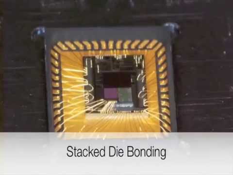
 NXP Automobile Microcontroller SPC560P54L5 Binary Restoration
NXP Automobile Microcontroller SPC560P54L5 Binary Restoration is a process to unlock nxp microprocessor spc560p54l5 protection over its flash memory, and then readout embedded firmware from microcomputer’s flash memory;
This 32-bit system-on-chip (SoC) automotive microcontroller family is the latest achievement in integrated automotive application controllers. It belongs to an expanding range of automotive-focused products designed to address chassis applications specifically the airbag application.
This family is one of a series of next-generation integrated automotive microcontrollers based on the Power Architecture technology when duplicating spc56el70l5 microcontroller flash memory content. The advanced and cost-efficient host processor core of this automotive controller family complies with the Power Architecture embedded category.
It operates up to 64 MHz and offers high performance processing optimized for low power consumption. It capitalizes on the available development infrastructure of current Power Architecture devices and is supported with software drivers, operating systems and configuration code to assist with users implementations.
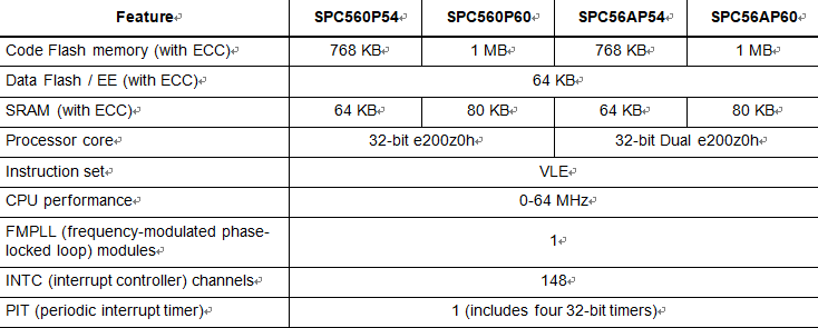
Below table provides a summary of different members of the SPC56xP54x/SPC56xP60x family and their features—relative to Full-featured version after copying freescale microcomputer spc564l70l3 flash binary—to enable a comparison among the family members and an understanding of the range of functionality offered within this family.
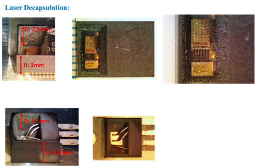
STM Locked Microcontroller SPC56EL54L7 Code Data Extraction
STM Locked Microcontroller SPC56EL54L7 Code Data Extraction needs to crack Microprocessor SPC56EL54 tamper resistance system by technique and then readout flash memory program from microcomputer;
The following list summarizes the key features of the flash memory controller:
- Single AHB port interface supports a 64-bit data bus. All AHB aligned and unaligned reads within the 32-bit container are supported. Only aligned word writes are supported.
- Array interfaces support a 128-bit read data bus and a 64-bit write data bus for each bank.
- Code flash (bank0) interface provides configurable read buffering and page prefetch support.
- Four page-read buffers (each 128 bits wide) and a prefetch controller support speculative reading and optimized flash access.
- Single-cycle read responses (0 AHB data-phase wait states) for hits in the buffers. The buffers implement a least-recently-used replacement algorithm to maximize performance.
- Data flash (bank1) interface includes a 128-bit register to temporarily hold a single flash page. This logic supports single-cycle read responses (0 AHB data-phase wait states) for accesses that hit in the holding register when clone spc56el54l5 microcontroller memory heximal file.
- No prefetch support is provided for this bank.
- Programmable response for read-while-write sequences including support for stall- while-write, optional stall notification interrupt, optional flash operation abort and optional abort notification interrupt.
- Separate and independent configurable access timing (on a per bank basis) to support use across a wide range of platforms and frequencies.
- Support of address-based read access timing for emulation of other memory types.
- Support for reporting of single- and multi-bit error events.
Typical operating configuration loaded into programming model by system reset in order to copy stmicro spc564l70l3 microcontroller flash binary. The platform flash controller is replicated for each processor.
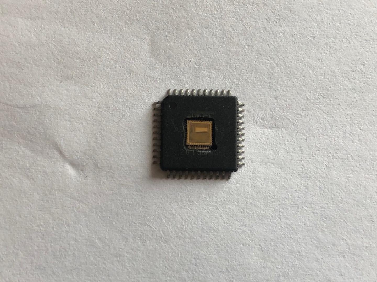
Clone STMicroelectronics SPC56EL54L5 Microcontroller Memory Heximal
Clone STMicroelectronics SPC56EL54L5 Microcontroller Memory Heximal from its secured flash memory, the extracted program can be rewritten to new MCU SPC56EL54L5 which can provide the same functions as original MCU, master microcontroller status will be decrypted from locked to unlocked one;
This device includes programmable, non-volatile flash memory. The non-volatile memory (NVM) can be used for instruction storage or data storage, or both. The flash memory module interfaces with the system bus through a dedicated flash memory array controller.
It supports a 64-bit data bus width at the system bus port, and a 128-bit read data interface to flash memory. The module contains four 128-bit prefetch buffers. Prefetch buffer hits allow no-wait responses. Buffer misses incur a 3 wait state response at 120 MHz as the consequence of copying freescale microprocessor spc564l70l3 memory binary.
The flash memory module provides the following features:
- 2 MB of flash memory in unique multi-partitioned hard macro
- Sectorization:
- Partition 1 (low address): 16 KB + 16 KB + 16 KB + 16 KB
- Partition 2 (low address): 16 KB + 16 KB + 16 KB + 16 KB
- Partition 3 (low address): 64 KB + 64 KB
- Partition 4 (mid address): 128 KB + 128 KB
- Partition 5 (high address): 256 KB + 256 KB
- Partition 6 (high address): 256 KB + 256 KB
- Partition 7 (high address): 256 KB + 256 KB
- EEPROM emulation (in software) within same module but on different partition
- 16 KB test sector and 16 KB shadow sector for test, censorship device and user option bits
- Wait states:
- Access time less or equal to 3 WS at 120 MHz + 4% FM (4-1-2-1 access)
- Access time less or equal to 2 WS at 80 MHz + 4% FM
- Flash memory line 128-bit wide with 8-bit ECC on 64-bit word (total 144 bits)
- Accessed via a 64-bit wide bus for write and a 128-bit wide array for read operations
- 1-bit error correction, 2-bit error detection
- Sectorization:
The SPC56XL70 SRAM provides a general-purpose single port memory
ECC handling is done on a 32-bit boundary for data and it is extended to the address to have the highest possible diagnostic coverage including the array internal address decoder and cloning spc564l70l5 mcu flash memory firmware.
The SRAM module provides the following features:
- System SRAM: 192 KB
- ECC on 32-bit word (syndrome of 7 bits)
- ECC covers SRAM bus address
- 1-bit error correction, 2-bit error detection
- Wait states:
- 1 wait state at 120 MHz
- 0 wait states at 80 MHz
- ECC on 32-bit word (syndrome of 7 bits)
STMicroelectronics SPC56EL54L3 Locked MCU Flash Memory Firmware Reading
STMicroelectronics SPC56EL54L3 Locked MCU Flash Memory Firmware Reading will require to disable the microcontroller protection by working with its communication protocol by cracking microprocessor spc56el54l3 fuse bit;
The enhanced direct memory access (eDMA) controller is a second-generation module capable of performing complex data movements via 16 programmable channels, with minimal intervention from the host processor.
The hardware micro architecture includes a DMA engine which performs source and destination address calculations, and the actual data movement operations, along with an SRAM-based memory containing the transfer control descriptors (TCD) for the channels when breaking freescale spc56el70l3 flash memory. This implementation is used to minimize the overall block size.
The eDMA module provides the following features:
16 channels supporting 8-, 16-, and 32-bit value single or block transfers
Support variable sized queues and circular buffered queue
Source and destination address registers independently configured to post-increment or stay constant
Support major and minor loop offset
Support minor and major loop done signals
DMA task initiated either by hardware requestor or by software
Each DMA task can optionally generate an interrupt at completion and retirement of the task in the processor of duplicating freescale microcontroller spc56el70l5 flash program;
Signal to indicate closure of last minor loop
Transfer control descriptors mapped inside the SRAM The eDMA controller is replicated for each processing channel.
Freescale MCU SPC564L70L5 Flash Memory Firmware Cloning
Freescale MCU SPC564L70L5 Flash Memory Firmware Cloning needs to extract embedded heximal file from microcontroller spc564l70l5 flash memory firstly after crack microprocessor spc564l70l5 tamper resistance system;
The XBAR multi-port crossbar switch supports simultaneous connections between four master ports and three slave ports. The crossbar supports a 32-bit address bus width and a 64-bit data bus width.
The crossbar allows four concurrent transactions to occur from any master port to any slave port, although one of those transfers must be an instruction fetch from internal flash memory.
If a slave port is simultaneously requested by more than one master port, arbitration logic selects the higher priority master and grants it ownership of the slave port only after the process of clone freescale encrypted mcu spc5602df1v flash data. All other masters requesting that slave port are stalled until the higher priority master completes its transactions.
The crossbar provides the following features:
- 4 masters and 3 slaves supported per each replicated crossbar
- Masters allocation for each crossbar: e200z4d core with two independent bus interface units (BIU) for I and D access (2 masters), one eDMA, one FlexRay
- Slaves allocation for each crossbar: a redundant flash-memory controller with 2 slave ports to guarantee maximum flexibility to handle Instruction and Data array, one redundant SRAM controller with 1 slave port each and 1 redundant peripheral bus bridge
- 32-bit address bus and 64-bit data bus
- Programmable arbitration priority
- Requesting masters can be treated with equal priority and are granted access to a slave port in round-robin method, based upon the ID of the last master to be granted access or a priority order can be assigned by software at application run time
- Temporary dynamic priority elevation of masters The XBAR is replicated for each processing channel.
- Masters allocation for each crossbar: e200z4d core with two independent bus interface units (BIU) for I and D access (2 masters), one eDMA, one FlexRay
The Memory Protection Unit splits the physical memory into 16 different regions. Each master (eDMA, FlexRay, CPU) can be assigned different access rights to each region after spc5601df1m microcontroller on chip flash content being readout.
- 16-region MPU with concurrent checks against each master access
- 32-byte granularity for protected address region
The memory protection unit is replicated for each processing channel.
Freescale Microcontroller SPC564L70L3 Flash Binary Copying
Freescale Microcontroller SPC564L70L3 Flash Binary Copying means the embedded firmware inside MCU SPC564L70L3 flash memory will be extracted after unlock microprocessor spc564l70l3 secured system over its memory system;
The advanced and cost- efficient host processor core of the SPC56XL70 automotive controller family complies with the Power Architecture embedded category. It operates at speeds as high as 120 MHz and offers high-performance processing optimized for low power consumption.
It capitalizes on the available development infrastructure of current Power Architecture devices and is supported with software drivers, operating systems and configuration code to assist with users’ implementations in the process of breaking spc56el70l3 microprocessor flash memory.
The e200z4d Power Architecture® core provides the following features:
- 2 independent execution units, both supporting fixed-point and floating-point operations
- Dual issue 32-bit Power Architecture technology compliant
- 5-stage pipeline (IF, DEC, EX1, EX2, WB)
- In-order execution and instruction retirement
- Full support for Power Architecture instruction set and Variable Length Encoding (VLE)
- Mix of classic 32-bit and 16-bit instruction allowed
- Optimization of code size possible
- Thirty-two 64-bit general purpose registers (GPRs)
- Harvard bus (32-bit address, 64-bit data)
- I-Bus interface capable of one outstanding transaction plus one piped with no wait- on-data return
- D-Bus interface capable of two transactions outstanding to fill AHB pipe
- I-cache and I-cache controller
- 4 KB, 256-bit cache line (programmable for 2- or 4-way)
- No data cache
- 16-entry MMU
- 8-entry branch table buffer
- Branch look-ahead instruction buffer to accelerate branching
- Dedicated branch address calculator
- 3 cycles worst case for missed branch
- Load/store unit
- Fully pipelined
- Single-cycle load latency
- Big- and little-endian modes supported
- Misaligned access support
- Single stall cycle on load to use
- Single-cycle throughput (2-cycle latency) integer 32 × 32 multiplication
- 4 – 14 cycles integer 32 × 32 division (average division on various benchmark of nine cycles)
- Single precision floating-point unit
- 1 cycle throughput (2-cycle latency) floating-point 32 × 32 multiplication
- Target 9 cycles (worst case acceptable is 12 cycles) throughput floating-point 32 × 32 division
- Special square root and min/max function implemented
- Signal processing support: APU-SPE 1.1
- Support for vectorized mode: as many as two floating-point instructions per clock
- Vectored interrupt support
- Dual issue 32-bit Power Architecture technology compliant
Reservation instruction to support read-modify-write constructs
Duplicating Freescale Microcontroller SPC56EL70L5 Flash Program
Duplicating Freescale Microcontroller SPC56EL70L5 Flash Program after crack freescale microprocessor spc56el70l5 protective system and extract embedded source code from MCU’s flash memory;
This document describes the features of the family and options available within the family members, and highlights important electrical and physical characteristics of the devices.
This document provides electrical specifications, pin assignments, and package diagrams for the SPC56EL70x/SPC564L70x series of microcontroller units (MCUs). For functional characteristics, see the SPC56XL70 Microcontroller Reference Manual.
For use of the SPC56XL70 in a fail-safe system according to safety standard ISO26262, see the Safety Application Guide for SPCEL70.
The SPC56EL70x/SPC564L70x series microcontrollers are system-on-chip devices that are built on Power Architecture technology and contain enhancements that improve the architecture’s fit in embedded applications which is important for replicating nxp mcu spc5604bk0c flash memory content, include additional instruction support for digital signal processing (DSP) and integrate technologies such as an enhanced time processor unit, enhanced queued analog-to-digital converter, Controller Area Network, and an enhanced modular input-output system.
The SPC56EL70x/SPC564L70x family of 32-bit microcontrollers is the latest achievement in integrated automotive application controllers which is important for cracking microcontroller spc5603bam114r locked bits. It belongs to an expanding range of automotive-focused products designed to address electrical hydraulic power steering (EHPS), electric power steering (EPS) and airbag applications.
Freescale SPC56EL70L3 Microprocessor Flash Program Breaking
Freescale SPC56EL70L3 Microprocessor Flash Program Breaking is a process to disable its tamper resistance system and readout microprocessor nxp spc56el70l3 flash memory program;
- High-performance e200z4d dual core
- 32-bit Power Architecture® technology CPU
- Core frequency as high as 120 MHz
- Dual issue five-stage pipeline core
- Variable Length Encoding (VLE)
- Memory Management Unit (MMU)
- 4 KB instruction cache with error detection code
- Signal Processing Engine (SPE)
- Memory available
- 2 MB flash memory with ECC
- 192 KB on-chip SRAM with ECC
- Built-in RWW capabilities for EEPROM emulation
- SIL3/ASILD innovative safety concept: Lock step mode and Fail-safe protection
- Sphere of Replication (SoR) for key components (such as CPU core, eDMA, crossbar switch)
- Fault Collection and Control Unit (FCCU)
- Redundancy Control and Checker Unit (RCCU) on outputs of the SoR connected to FCCU
- Boot-time Built-In Self-Test for Memory (MBIST) and Logic (LBIST) triggered by hardware
- Boot-time Built-In Self-Test for ADC and flash memory triggered by software which can be applied for recover nxp spc5603bk03 microcomputer flash file;
Replicated safety enhanced watchdog
- Replicated junction temperature sensor
- Non Maskable Interrupt (NMI)
- 16-region Memory Protection Unit (MPU)
- Clock Monitoring Units (CMU)
- Power Management Unit (PMU)
- Cyclic Redundancy Check (CRC) unit
- Decoupled Parallel mode for high performance use of replicated cores
- Nexus Class 3+ interface
- Interrupts
- Replicated 16-priority controller
- Replicated 16-channel eDMA controller
- GPIOs individually programmable as input, output or special function
- Three 6-channel general-purpose eTimer units can be used for restoring microcomputer spc5603ck0c flash content
- 2 FlexPWM units: Four 16-bit channels per module
- Communications interfaces
- 2 LINFlexD channels
- 3 DSPI channels with automatic chip select generation
- 3 FlexCAN interfaces (2.0B Active) with 32 message objects
- FlexRay module (V2.1 Rev. A) with 2 channels, 64 message buffers and data rates up to 10 Mbit/s
- Two 12-bit Analog-to-digital Converters (ADC)
- 16 input channels
- Programmable Cross Triggering Unit (CTU) to synchronize ADCs conversion with timer and PWM
- Sine wave generator (D/A with low pass filter)
- On-chip CAN/UART/FlexRay Bootstrap loader
- Single 3.0 V to 3.6 V voltage supply
- Ambient temperature range –40 °C to 125 °C
Junction temperature range –40 °C to 150 °C
ST Microcomputer ST72F340K2 Flash Program Memory Unlocking
ST Microcomputer ST72F340K2 Flash Program Memory Unlocking needs to disable the fuse bit of tamper resistance system and readout embedded firmware from Microcontroller, pull extracted heximal to new st72f340k2 microprocessor flash memory;
To perform ICP the microcontroller must be switched to ICC (In-Circuit Communication) mode by an external controller or programming tool.
Depending on the ICP code downloaded in RAM, Flash memory programming can be fully customized (number of bytes to program, program locations, or selection serial communication interface for downloading) when copy embedded binary firmware to new microcontroller st72f325s6.
When using an STMicroelectronics or third-party programming tool that supports ICP and the specific microcontroller device, the user needs only to implement the ICP hardware interface on the application board (see below Figure). For more details on the pin locations, refer to the device pinout description.
This mode uses a BootLoader program previously stored in Sector 0 by the user (in ICP mode or by plugging the device in a programming tool). This mode is fully controlled by user software in the process of cloning st72f325k4 secured microcontroller flash memory content. This allows it to be adapted to the user application, (us- er-defined strategy for entering programming mode, choice of communications protocol used to fetch the data to be stored, etc.).
NXP Locked Microcontroller SPC5604PGF1VLQ6 Flash Data Duplication
NXP Locked Microcontroller SPC5604PGF1VLQ6 Flash Data Duplication needs to crack spc5604pgf1vl mcu protective system and extract embedded flash binary from microcomputer’s memory:
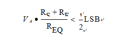
In fact a current sink contributor is represented by the charge sharing effects with the sampling capacitance: being CS and Cp2 substantially two switched capacitances, with a frequency equal to the conversion rate of the ADC, it can be seen as a resistive path to ground when recover spc5603bk microcomputer flash file.
For instance, assuming a conversion rate of 1 MHz, with CS+Cp2 equal to 3 pF, a resistance of 330 kW is obtained (REQ = 1 / (fc × (CS+Cp2)), where fc represents the conversion rate at the considered channel). To minimize the error induced by the voltage partitioning between this resistance (sampled voltage on CS+Cp2) and the sum of RS + RF, the external circuit must be designed to respect the below Equation:
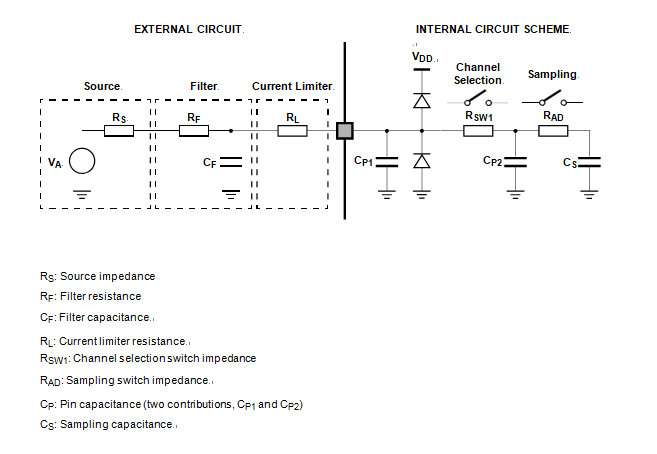
A second aspect involving the capacitance network shall be considered. Assuming the three capacitances CF, CP1 and CP2 are initially charged at the source voltage VA (refer to the equivalent circuit in Figure 13): A charge sharing phenomenon is installed when the sampling phase is started (A/D switch close).