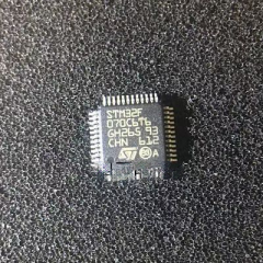
ARM Microcontroller STM32F071C8 Heximal Program Recovery
ARM Microcontroller STM32F071C8 Heximal Program Recovery can help engineer to take the heximal file from stm32f071c8 mcu after crack microcontroller’s tamper resistance system, disable readout protection over chip stm32f071c8 and extract its source code from its flash memory;
System clock selection is performed on startup, however the internal RC 8 MHz oscillator is selected as default CPU clock on reset. An external 4-32 MHz clock can be selected, in which case it is monitored for failure. If failure is detected, the system automatically switches back to the internal RC oscillator.
Восстановление гексимальной программы микроконтроллера ARM STM32F071C8 может помочь инженеру взять шестигранный файл из микроконтроллера stm32f071c8 после взлома системы защиты от несанкционированного доступа микроконтроллера, отключить защиту от считывания на чипе stm32f071c8 и извлечь его исходный код из флэш-памяти;
A software interrupt is generated if enabled. Similarly, full interrupt management of the PLL clock entry is available when necessary (for example on failure of an indirectly used external crystal, resonator or oscillator) when break arm microcontroller stm32f101rb flash memory. Several prescalers allow the application to configure the frequency of the AHB and the APB domains. The maximum frequency of the AHB and the APB domains is 48 MHz.
Each of the GPIO pins can be configured by software as output (push-pull or open-drain), as input (with or without pull-up or pull-down) or as peripheral alternate function in order to recover arm microcontroller stm32f101c4 locked firmware. Most of the GPIO pins are shared with digital or analog alternate functions. The I/O configuration can be locked if needed following a specific sequence in order to avoid spurious writing to the I/Os registers.
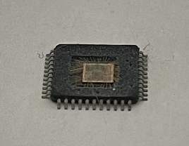
ARM STM32F071CB Microcontroller Flash Binary Restoration
ARM STM32F071CB Microcontroller Flash Binary Restoration needs to crack arm mcu ic stm32f071cb readout protection and then copy locked flash binary to new microcontroller stm32f071cb.
The regulator has two operating modes and it is always enabled after reset.
- Main (MR) is used in normal operating mode (Run).
- Low power (LPR) can be used in Stop mode where the power demand is reduced.
In Standby mode, it is put in power down mode. In this mode, the regulator output is in high impedance and the kernel circuitry is powered down, inducing zero consumption (but the contents of the registers and SRAM are lost).
The STM32F070CB/RB/C6/F6 microcontrollers support three low-power modes to achieve the best compromise between low power consumption, short startup time and available wakeup sources in the process of breaking stm32f070c6 chip flash memory locking bit:
· Sleep mode
In Sleep mode, only the CPU is stopped. All peripherals continue to operate and can wake up the CPU when an interrupt/event occurs.
· Stop mode
Stop mode achieves very low power consumption while retaining the content of SRAM and registers. All clocks in the 1.8 V domain are stopped, the PLL, the HSI RC and the HSE crystal oscillators are disabled. The voltage regulator can also be put either in normal or in low power mode.
The device can be woken up from Stop mode by any of the EXTI lines. The EXTI line source can be one of the 16 external lines and RTC.
· Standby mode
The Standby mode is used to achieve the lowest power consumption. The internal voltage regulator is switched off so that the entire 1.8 V domain is powered off. The PLL, the HSI RC and the HSE crystal oscillators are also switched off for the sake of cracking stm32f070cb mcu flash memory protection. After entering Standby mode, SRAM and register contents are lost except for registers in the RTC domain and Standby circuitry.
Восстановление двоичного файла флэш-памяти микроконтроллера ARM STM32F071CB необходимо взломать защиту от считывания микросхемы микроконтроллера ARM STM32F071CB, а затем скопировать заблокированный двоичный файл флэш-памяти на новый микроконтроллер STM32F071CB.
The device exits Standby mode when an external reset (NRST pin), an IWDG reset, a rising edge on the WKUP pins, or an RTC event occurs.
Note: The RTC, the IWDG, and the corresponding clock sources are not stopped by entering Stop or Standby mode.
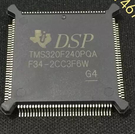
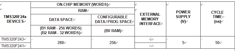
Recover Texas Instrument DSP TMS320F240PQG4 MCU Flash Software
Recover Texas Instrument DSP TMS320F240PQG4 MCU Flash Software needs to unlock dsp microcontroller tms32f240pqg4 security fuse bit, copy heximal file to new microprocessor tms320f240pqg4 to make MCU cloning;
The TMS320F243 and TMS320F241 devices are members of the 24x generation of digital signal processor (DSP) controllers based on the TMS320C2000™ platform of 16-bit fixed-point DSPs. The F243 is a superset of the F241. These two devices share similar core and peripherals with some exceptions by breaking dsp controller tms320f240 flash memory.
For example, the F241 does not have an external memory interface. This new family is optimized for digital motor/ motion control applications.
восстановить программное обеспечение флэш-памяти микроконтроллера Texas Instrument DSP TMS320F240PQG4, необходимое для разблокировки предохранителя микроконтроллера DSP tms32f240pqg4, копирования шестигранного файла на новый микропроцессор tms320f240pqg4 для клонирования MCU;
The DSP controllers combine the enhanced TMS320™ DSP family architectural design of the C2xx core CPU for low-cost, high-performance processing capabilities and several advanced peripherals optimized for motor / motion control applications.
These peripherals include the event manager module, which provides general-purpose timers and PWM registers to generate PWM outputs, and a single,10-bit analog-to-digital converter (ADC), which can perform conversion within 1 ms by attacking tms320f243pge ti microprocessor protection.
Attack STMicrocontroller STM32F070F6 IC Readout-Protection
Attack STMicrocontroller STM32F070F6 IC Readout-Protection in order to reset the fuse bit and change the status of chip itself, then restore embedded program from mcu stm32f070f6 flash memory in the format of binary, copy this binary file to new arm processor stm32f070f6;
The CRC (cyclic redundancy check) calculation unit is used to get a CRC code using a configurable generator polynomial value and size. Among other applications, CRC-based techniques are used to verify data transmission or storage integrity.
атаковать STMicrocontroller STM32F070F6 IC readout-protection с целью сброса бита предохранителя и изменения состояния самого чипа, затем восстановить встроенную программу из флэш-памяти MCU STM32F070F6 в формате двоичного файла, скопировать этот двоичный файл на новый процессор ARM STM32F070F6;
In the scope of the EN/IEC 60335-1 standard, they offer a means of verifying the Flash memory integrity. The CRC calculation unit helps compute a signature of the software during runtime, to be compared with a reference signature generated at link-time and stored at a given memory location when attacking stm32f070rb arm mcu locked bits.
- VDD = 2.4 to 3.6 V: external power supply for I/Os and the internal regulator. Provided externally through VDD pins.
- VDDA = from VDD to 3.6 V: external analog power supply for ADC, Reset blocks, RCs and PLL. The VDDA voltage level must be always greater or equal to the VDD voltage level and must be provided first.
For more details on how to connect power pins.
The device has integrated power-on reset (POR) and power-down reset (PDR) circuits. They are always active, and ensure proper operation above a threshold of 2 V. The device remains in reset mode when the monitored supply voltage is below a specified threshold, VPOR/PDR, without the need for an external reset circuit in the process of breaking stm32f070cb mcu flash memory.
- The POR monitors only the VDD supply voltage. During the startup phase it is required that VDDA should arrive first and be greater than or equal to VDD.
- The PDR monitors both the VDD and VDDA supply voltages, however the VDDA power supply supervisor can be disabled (by programming a dedicated Option bit) to reduce the power consumption if the application design ensures that VDDA is higher than or equal to VDD.
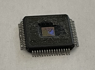
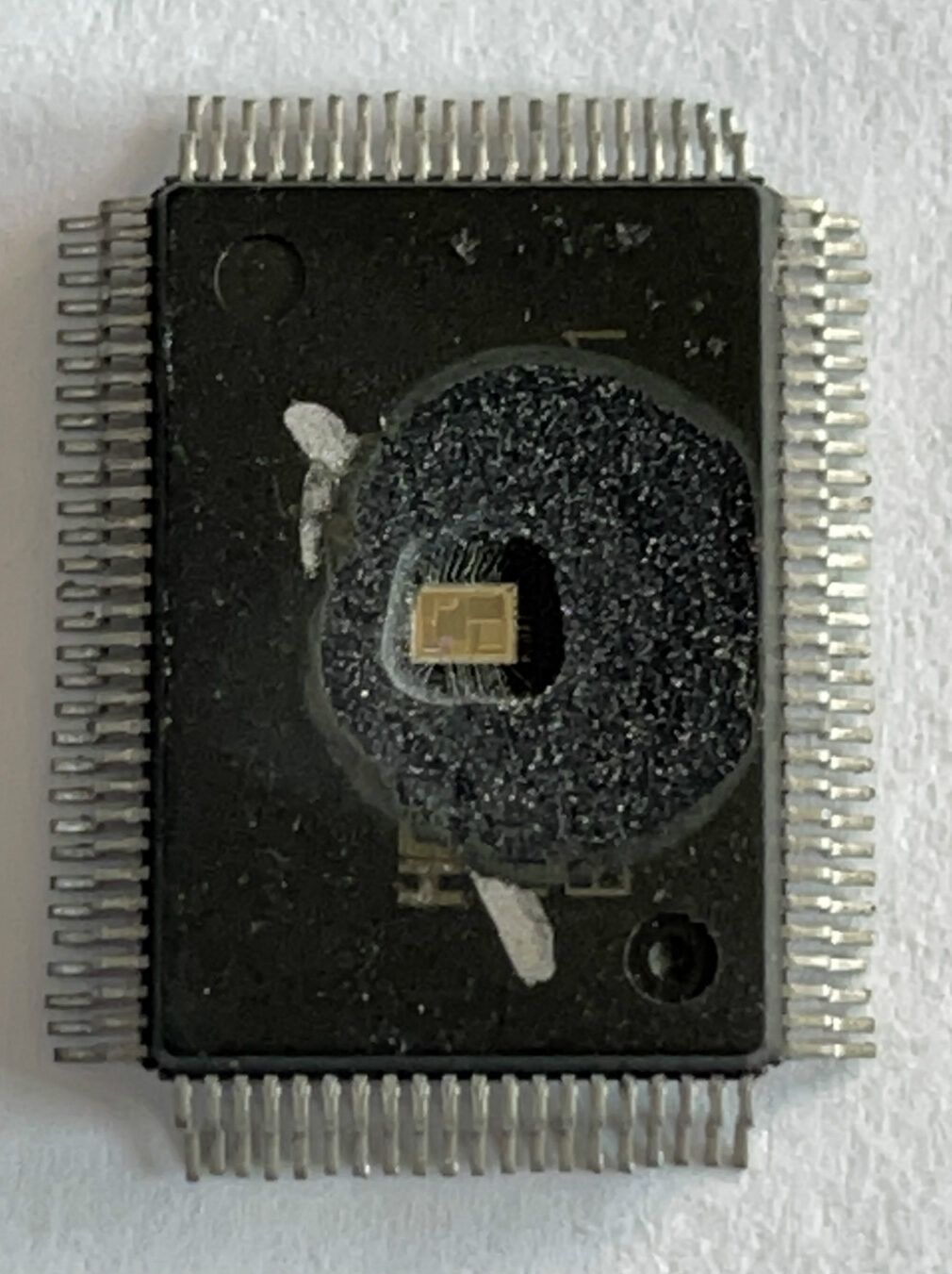
Break STMicroelectronics ARM STM32F070C6 MCU Memory
Break STMicroelectronics ARM STM32F070C6 MCU Memory will needs to use crack locked bits of microcontroller stm32f070c6 by focus ion beam to disable the protected status, extract embedded firmware from flash memory;
The ARM® Cortex®-M0 processor is the latest generation of ARM processors for embedded systems. It has been developed to provide a low-cost platform that meets the needs of MCU implementation, with a reduced pin count and low-power consumption, while delivering outstanding computational performance and an advanced system response to interrupts.
The ARM® Cortex®-M0 32-bit RISC processor features exceptional code-efficiency, delivering the high-performance expected from an ARM core in the memory size usually associated with 8- and 16-bit devices. The STM32F0xx family has an embedded ARM core and is therefore compatible with all ARM tools and software which become easier when trying to replicate arm mcu stm32f105r8 flash program file.
сломать память микроконтроллера STMicroelectronics ARM STM32F070C6, которая должна будет использовать заблокированные биты микроконтроллера STM32F070C6 путем фокусировки ионного луча, чтобы отключить защищенное состояние, извлечь встроенную прошивку из флэш-памяти;
The device has the following features:
- 6 to 16 Kbytes of embedded SRAM accessed (read/write) at CPU clock speed with 0 wait states and featuring embedded parity checking with exception generation for fail- critical applications.
- The non-volatile memory is divided into two arrays:
- 32 to 128 Kbytes of embedded Flash memory for programs and data
- Option bytes
- The non-volatile memory is divided into two arrays:
The option bytes are used to write-protect the memory (with 4 KB granularity) and/or readout-protect the whole memory with the following options:
- Level 0: no readout protection
- Level 1: memory readout protection, the Flash memory cannot be read from or written to if either debug features are connected or boot in RAM is selected
- Level 2: chip readout protection, debug features (Cortex®-M0 serial wire) and boot in RAM selection disabled, through our technique we can unlock secured mcu stm32f070rc flash memory
- Level 1: memory readout protection, the Flash memory cannot be read from or written to if either debug features are connected or boot in RAM is selected
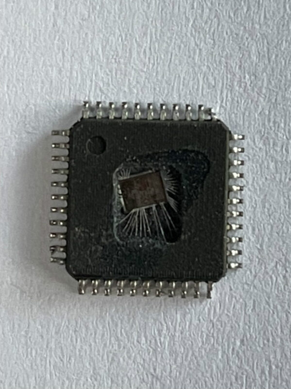
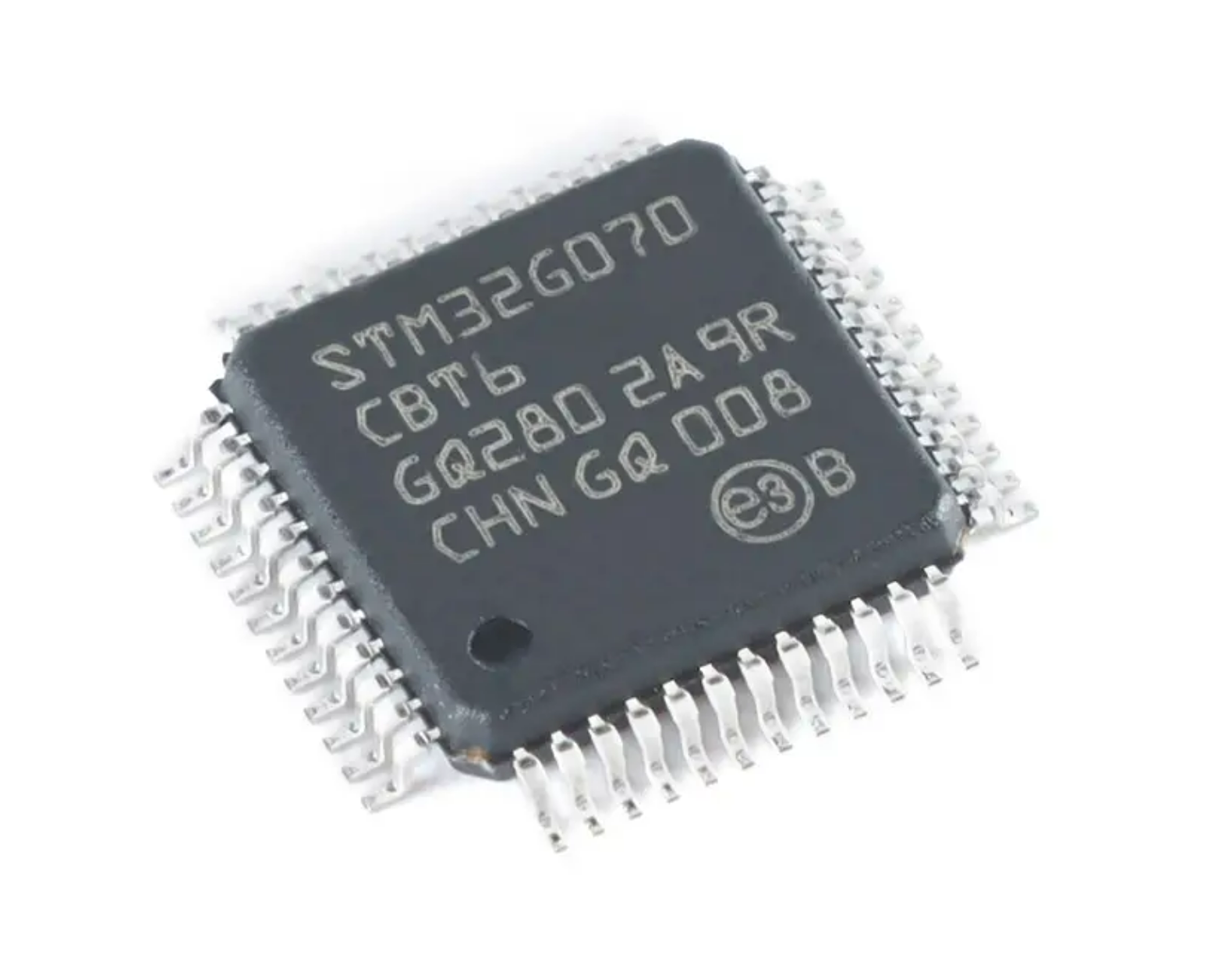
Attack ARM Cortex M0 CPU STM32F070RBT6 Locked Bits
Attack ARM Cortex M0 CPU STM32F070RBT6 Locked Bits and disable the tamper resistance system of microcontroller stm32f070rbt6, the embedded firmware inside flash memory can be extracted from microprocessor stm32f070rbt6 in the exactly same format of originals;
The STM32F070CB/RB/C6/F6 microcontrollers incorporate the high-performance ARM® Cortex®-M0 32-bit RISC core operating at a 48 MHz frequency, high-speed embedded
memories (up to 128 Kbytes of Flash memory and up to 16 Kbytes of SRAM), and an extensive range of enhanced peripherals and I/Os. All devices offer standard communication interfaces which can be used for cracking arm mcu stm32f071vct6 protection (up to two I2Cs, up to two SPIs and up to four USARTs), one USB Full speed device, one 12-bit ADC, seven general-purpose 16-bit timers and an advanced- control PWM timer.
حمله ARM Cortex M0 CPU STM32F070RBT6 بیت های قفل شده و غیر فعال کردن سیستم مقاومت در برابر دستکاری میکروکنترلر stm32f070rbt6، سیستم عامل تعبیه شده در داخل حافظه فلش را می توان از میکروپروسسور stm32f070rbt6 دقیقا در همان فرمت اصلی استخراج کرد.
The STM32F070CB/RB/C6/F6 microcontrollers operate in the -40 to +85 °C temperature range from a 2.4 to 3.6V power supply. A comprehensive set of power-saving modes allows the design of low-power applications.
The STM32F070CB/RB/C6/F6 microcontrollers include devices in three different packages ranging from 20 pins to 64 pins. Depending on the device chosen, different sets of peripherals are included. The description below provides an overview of the complete range of STM32F070CB/RB/C6/F6 peripherals proposed.
These features make the STM32F070CB/RB/C6/F6 microcontrollers suitable for a wide range of applications such as application control and user interfaces, handheld equipment, A/V receivers and digital TV, PC peripherals, gaming and GPS platforms, industrial applications, PLCs, inverters, printers, scanners, alarm systems, video intercoms, and HVACs.
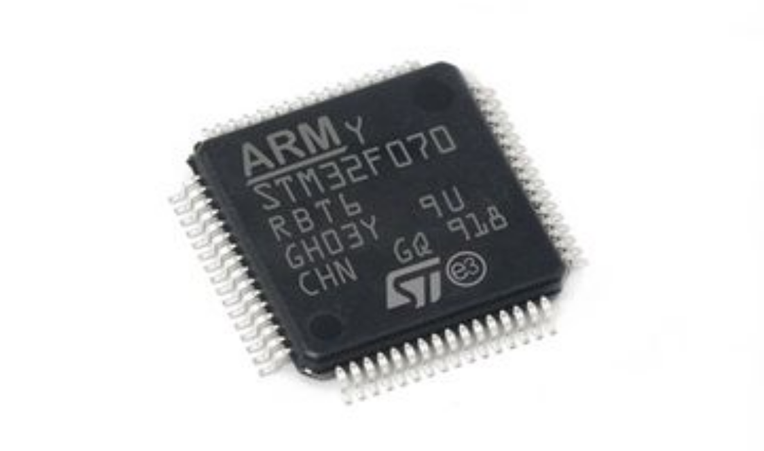
32-Bit STM32F070CBT6 IC MCU Flash Cracking
32-Bit STM32F070CBT6 IC MCU Flash Cracking will help engineer to restore embedded firmware of microcontroller stm32f070cbt6 in the format of binary or heximal, and copy extracted content to new processor stm32f070cbt6;
- Core: ARM® 32-bit Cortex®-M0 CPU, frequency up to 48 MHz
- Memories
- 32 to 128 Kbytes of Flash memory
- 6 to 16 Kbytes of SRAM with HW parity
- CRC calculation unit
- Reset and power management is a kind of technique can be used for unlocking arm cortex stm32f070 mcu flash program
- Digital & I/Os supply: VDD = 2.4 V to 3.6 V
- Analog supply: VDDA = VDD to 3.6 V
- Power-on/Power down reset (POR/PDR)
- Low power modes: Sleep, Stop, Standby
ترک خوردگی فلش 32 بیتی STM32F070CBT6 IC MCU به مهندس کمک خواهد کرد تا سیستم عامل تعبیه شده میکروکنترلر stm32f070cbt6 را در قالب باینری یا هگزیمال بازگرداند و محتوای استخراج شده را به پردازنده جدید stm32f070cbt6 کپی کند.
- Clock management
- 4 to 32 MHz crystal oscillator
- 32 kHz oscillator for RTC with calibration
- Internal 8 MHz RC with x6 PLL option
- Internal 40 kHz RC oscillator
- Up to 51 fast I/Os
- All mappable on external interrupt vectors
- Up to 51 I/Os with 5V tolerant capability
- 5-channel DMA controller
- One 12-bit, 1.0 µs ADC (up to 16 channels)
- Conversion range: 0 to 3.6 V
- Separate analog supply: 2.4 V to 3.6 V
- Calendar RTC with alarm and periodic wakeup from Stop/Standby
- 11 timers
- One 16-bit advanced-control timer for six-channel PWM output
- Up to seven 16-bit timers, with up to four IC/OC, OCN, usable for IR control decoding and cracking mcu stm32f071vct6 protection
- Independent and system watchdog timers
- SysTick timer
- Communication interfaces
- Up to two I2C interfaces
- Fast Mode Plus (1 Mbit/s) support, with 20 mA current sink
- SMBus/PMBus support (on single I/F)
- Up to four USARTs supporting master synchronous SPI and modem control; one with auto baud rate detection
- Up to two SPIs (18 Mbit/s) with 4 to 16 programmable bit frames
- USB 2.0 full-speed interface with BCD and LPM support
- Serial wire debug (SWD)
- All packages ECOPACK®2
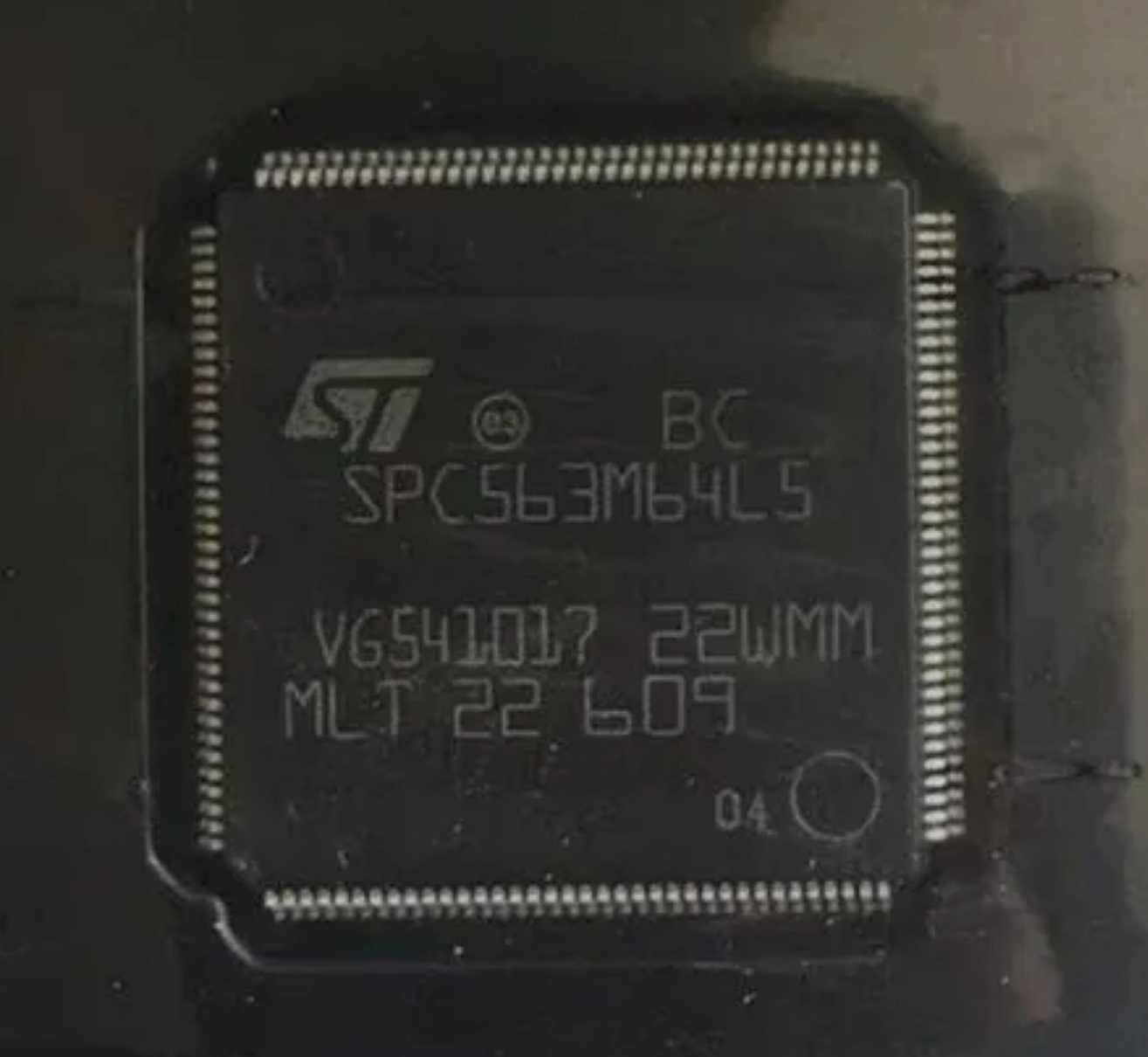
STMicroelectronics SPC56EL60L3 Microprocessor Flash Memory Breaking
STMicroelectronics SPC56EL60L3 Microprocessor Flash Memory Breaking needs to find a proper way to unlock tamper resistance mechanism of mcu spc56el60l3 and then extract embedded heximal file from its flash memory;
The main oscillator provides these features:
- Input frequency range 4–40 MHz
- Crystal input mode
- External reference clock (3.3 V) input mode
- FMPLL reference
The architecture uses constant current charging of a capacitor. The voltage at the capacitor is compared to the stable bandgap reference voltage. The RC oscillator is the device safe clock.
STMicroelectronics SPC56EL60L3 شکستن حافظه فلش ریزپردازنده نیاز به پیدا کردن یک راه مناسب برای باز کردن مکانیسم مقاومت در برابر دستکاری mcu spc56el60l3 و سپس استخراج فایل هگزیمال جاسازی شده از حافظه فلش ان
The RC oscillator provides these features:
- Nominal frequency 16 MHz
- ±5% variation over voltage and temperature after process trim
- Clock output of the RC oscillator serves as system clock source in case loss of lock or loss of clock is detected by the FMPLL when clone stmicro spc56el54l5 microcontroller memory heximal;
- RC oscillator is used as the default system clock during startup and can be used as back-up input source of FMPLL(s) in case XOSC fails
These modules provide the following:
- Clock gating and clock distribution control
- Halt, stop mode control
- Flexible configurable system and auxiliary clock dividers
- Various execution modes
- HALT and STOP mode as reduced activity low power mode
- Reset, Idle, Test, Safe
- Various RUN modes with software selectable powered modules
- No stand-by mode implemented (no internal switchable power domains)
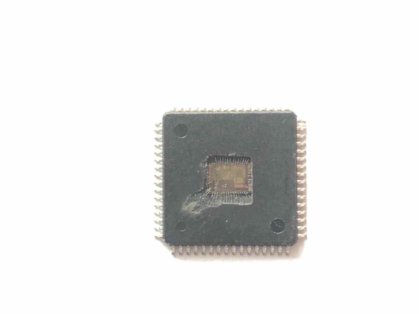
Automobile Microprocessor SPC56EL64 Embedded Program Extraction
Automobile Microprocessor SPC56EL64 Embedded Program Extraction is a process to extract flash heximal file from MCU flash memory after crack microcontroller spc56el64 protective system;
The following list summarizes the system clock and clock generation on this device:
- Lock status continuously monitored by lock detect circuitry
- Loss-of-clock (LOC) detection for reference and feedback clocks
- On-chip loop filter (for improved electromagnetic interference performance and fewer external components required)
- Programmable output clock divider of system clock (¸1, ¸2, ¸4, ¸8)
- FlexPWM module and as many as three eTimer modules running on an auxiliary clock independent from system clock (with max frequency 120 MHz)
- On-chip crystal oscillator with automatic level control
- Dedicated internal 16 MHz internal RC oscillator for rapid start-up
- Supports automated frequency trimming by hardware during device startup and by user application
- Auxiliary clock domain for motor control periphery (FlexPWM, eTimer, CTU, ADC, and SWG)
Each device has two FMPLLs.
otomobil mikroişlemcisi SPC56EL64 gömülü program Ekstraksiyon mikrodenetleyici spc56el64 koruyucu sistem çatlak sonra MCU flash bellekten flash onaltılık dosya ayıklamak için bir işlemdir
Each FMPLL allows the user to generate high speed system clocks starting from a minimum reference of 4 MHz input clock. Further, the FMPLL supports programmable frequency modulation of the system clock by reading spc56el54l3 mcu flash memory firmware. The FMPLL multiplication factor, output clock divider ratio are all software configurable. The FMPLLs have the following major features:
- Input frequency: 4–40 MHz continuous range (limited by the crystal oscillator)
- Voltage controlled oscillator (VCO) range: 256–512 MHz
- Frequency modulation via software control to reduce and control emission peaks
- Modulation depth ±2% if centered or 0% to –4% if downshifted via software control register
- Modulation frequency: triangular modulation with 25 KHz nominal rate
- Option to switch modulation on and off via software interface
- Reduced frequency divider (RFD) for reduced frequency operation without re-lock after duplicating microprocessor spc56el70l5 flash program
- 3 modes of operation
- Bypass mode
- Normal FMPLL mode with crystal reference (default)
- Normal FMPLL mode with external reference
- Lock monitor circuitry with lock status
- Loss-of-lock detection for reference and feedback clocks
- Self-clocked mode (SCM) operation
- On-chip loop filter
- Auxiliary FMPLL
- Used for FlexRay due to precise symbol rate requirement by the protocol
- Used for motor control periphery and connected IP (A/D digital interface CTU) to allow independent frequencies of operation for PWM and timers and jitter-free control
32 Bit Power Architecture MCU SPC56AP54L5 Flash Memory Recovery
32 Bit Power Architecture MCU SPC56AP54L5 Flash Memory Recovery means embedded heximal will be readout from locked flash memory of microcontroller spc56ap54l5, original status of microprocessor SPC56AP54L5 can be unlocked by MCU cracking technique;
The e200z0h Power Architecture core provides the following features:
32-битная архитектура питания MCU SPC56AP54L5 восстановление флэш-памяти означает, что встроенный гекзимал будет считываться из заблокированной флэш-памяти микроконтроллера SPC56AP54L5, исходное состояние микропроцессора SPC56AP54L5 может быть разблокировано с помощью метода взлома MCU
- High performance e200z0 core processor for managing peripherals and interrupts
- Single issue 4-stage pipeline in-order execution 32-bit Power Architecture CPU
- Harvard architecture
- Variable length encoding (VLE), allowing mixed 16-bit and 32-bit instructions
- Results in smaller code size footprint
- Minimizes impact on performance
- Branch processing acceleration using lookahead instruction buffer
- Load/store unit in the process of cloning of stm microcontroller spc56el54l5 memory data
- 1-cycle load latency
- Misaligned access support
- No load-to-use pipeline bubbles
- Thirty-two 32-bit general purpose registers (GPRs)
- Separate instruction bus and load/store bus Harvard architecture
- Hardware vectored interrupt support
- Reservation instructions for implementing read-modify-write constructs
- Long cycle time instructions, except for guarded loads, do not increase interrupt latency
- Extensive system development support through Nexus debug port
- Non maskable Interrupt support