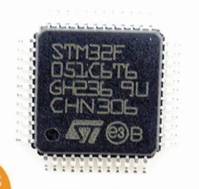
 Arm Microcontroller STM32F071V8 Source Code Decryption
Arm Microcontroller STM32F071V8 Source Code Decryption will be able to decode embedded firmware in the format of heximal from flash memory of stm32f071v8 mcu to universal version, but the original flash program must be extracted from stm32f071v8 microprocessor;
The system window watchdog is based on a 7-bit downcounter that can be set as free running. It can be used as a watchdog to reset the device when a problem occurs. It is clocked from the APB clock (PCLK). It has an early warning interrupt capability and the counter can be frozen in debug mode.
This timer is dedicated to real-time operating systems, but could also be used as a standard down counter. It features:
- A 24-bit down counter
- Autoreload capability
- Maskable system interrupt generation when the counter reaches 0
Programmable clock source (HCLK or HCLK/8)
Arm mikrodenetleyici STM32F071V8 kaynak kodu şifre çözme, STM32F071V8 MCU’nun flash belleğinden evrensel sürüme onaltılık formatta gömülü bellenimin kodunu çözebilecektir, ancak orijinal flash programı STM32F071V8 mikroişlemcisinden çıkarılmalıdır;
The RTC is an independent BCD timer/counter which can be applied for recover stm32f071c8 microprocessor flash program file. Its main features are the following:
- Calendar with subseconds, seconds, minutes, hours (12 or 24 format), week day, date, month, year, in BCD (binary-coded decimal) format.
- Automatic correction for 28, 29 (leap year), 30, and 31 day of the month.
- Programmable alarm with wake up from Stop and Standby mode capability.
- Periodic wakeup unit with programmable resolution and period.
- On-the-fly correction from 1 to 32767 RTC clock pulses. This can be used to synchronize the RTC with a master clock.
- Digital calibration circuit with 1 ppm resolution, to compensate for quartz crystal inaccuracy to effectively prevent the stm32f071r8 mcu flash memory unauthorized breaking;
- Tow anti-tamper detection pins with programmable filter. The MCU can be woken up from Stop and Standby modes on tamper event detection.
- Timestamp feature which can be used to save the calendar content. This function can be triggered by an event on the timestamp pin, or by a tamper event. The MCU can be woken up from Stop and Standby modes on timestamp event detection.
- Reference clock detection: a more precise second source clock (50 or 60 Hz) can be used to enhance the calendar precision.
The RTC clock sources can be:
- A 32.768 kHz external crystal
- A resonator or oscillator
- The internal low-power RC oscillator (typical frequency of 40 kHz)
The high-speed external clock divided by 32
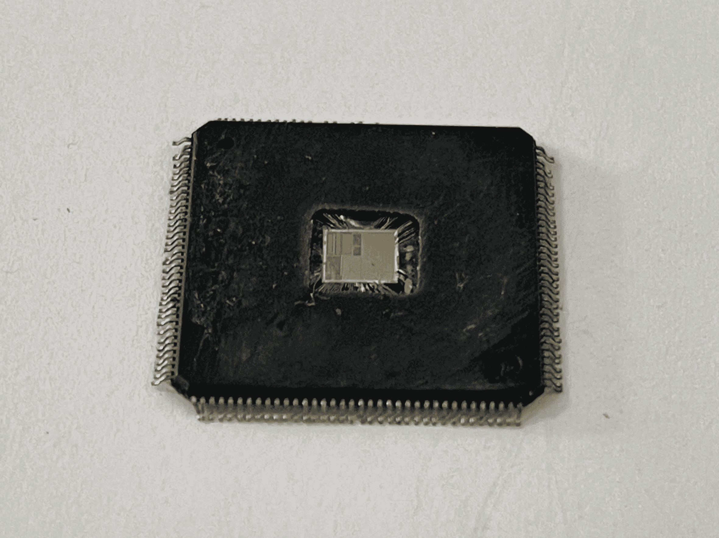
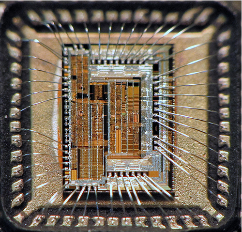
Break ARM STM32F071R8 Microcontroller Flash Memory
Break ARM STM32F071R8 Microcontroller Flash Memory protection and readout embedded heximal file from mcu stm32f071rb chip, then tamper resistance system of microprocessor stm32f071rb will be unlocked;
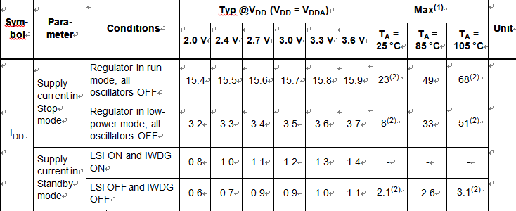
The current consumption is a function of several parameters and factors such as the operating voltage, ambient temperature, I/O pin loading, device software configuration, operating frequencies, I/O pin switching rate, program location in memory and executed binary code.
The current consumption is measured as described in Figure 13: Current consumption measurement scheme. All Run-mode current consumption measurements given in this section are performed with a reduced code that gives a consumption equivalent to CoreMark code after recover stm32f071c8 locked mcu flash memory content.
The MCU is placed under the following conditions:
- All I/O pins are in analog input mode
- All peripherals are disabled except when explicitly mentioned
- The Flash memory access time is adjusted to the fHCLK frequency:
- 0 wait state and Prefetch OFF from 0 to 24 MHz
- 1 wait state and Prefetch ON above 24 MHz
- When the peripherals are enabled fPCLK = fHCLK
The parameters given in to below Table are derived from tests performed under ambient temperature and supply voltage conditions summarized in Table 24: General operating conditions.
ARM STM32F071R8 mikrodenetleyici flash bellek korumasını kırın ve mcu stm32f071rb çipinden gömülü onaltılık dosyayı okuyun, daha sonra mikroişlemcinin kurcalama direnci sistemi stm32f071rb kilidi açılacaktır;
ARM Microprocessor STM32F071R8 Flash Code Restoration
ARM Microprocessor STM32F071R8 Flash Code Restoration can help engineer to crack flash memory content from arm mcu stm32f071rb and then copy heximal file to new microcontroller stm32f071rb;
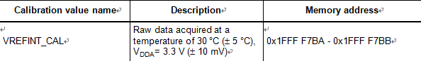
The internal voltage reference (VREFINT) provides a stable (bandgap) voltage output for the ADC. VREFINT is internally connected to the ADC_IN17 input channel. The precise voltage of VREFINT is individually measured for each part by ST during production test and stored in the system memory area. It is accessible in read-only mode.
The advanced-control timer (TIM1) can be seen as a three-phase PWM multiplexed on six channels. It has complementary PWM outputs with programmable inserted dead times after cracking stm32f070cb flash memory. It can also be seen as a complete general-purpose timer. The four independent channels can be used for:
ARM mikroişlemci STM32F071R8 flaş kodu geri yükleme, mühendisin ARM MCU STM32F071RB’den flash bellek içeriğini kırmasına ve ardından onaltılık dosyayı yeni mikrodenetleyici STM32F071RB’ye kopyalamasına yardımcı olabilir;
- Input capture
- Output compare
- PWM generation (edge or center-aligned modes)
- One-pulse mode output
If configured as a standard 16-bit timer, it has the same features as the TIMx timer. If configured as the 16-bit PWM generator, it has full modulation capability (0-100%).
The counter can be frozen in debug mode. Many features are shared with those of the standard timers which have the same architecture. The advanced control timer in the process of restore arm microprocessor stm32f071cb flash binary can therefore work together with the other timers via the Timer Link feature for synchronization or event chaining.
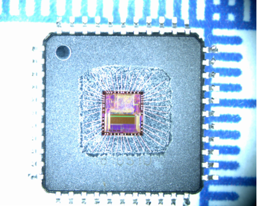
ARM Locked CPU STM32F071RB Flash Data Recovery
In order to execute ARM Locked CPU STM32F071RB Flash Data Recovery, status of microcontroller stm32f071rb will be reset from locked to unlocked and then read embedded software out directly from MCU’s flash memory;
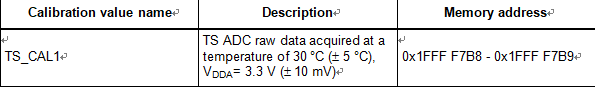
The temperature sensor (TS) generates a voltage VSENSE that varies linearly with temperature.
The temperature sensor is internally connected to the ADC_IN16 input channel which is used to convert the sensor output voltage into a digital value.
The sensor provides good linearity but it has to be calibrated to obtain good overall accuracy of the temperature measurement. As the offset of the temperature sensor varies from chip to chip due to process variation, the uncalibrated internal temperature sensor is suitable for applications that detect temperature changes only.
To improve the accuracy of the temperature sensor measurement, each device is individually factory-calibrated by ST. The temperature sensor factory calibration data are stored by ST in the system memory area, accessible in read-only mode.
The CRC (cyclic redundancy check) calculation unit is used to get a CRC code using a configurable generator polynomial value and size. Among other applications, CRC-based techniques are used to verify data transmission or storage integrity.
In the scope of the EN/IEC 60335-1 standard, they offer a means of verifying the Flash memory integrity. The CRC calculation unit helps compute a signature of the software during runtime, to be compared with a reference signature generated at link- time and stored at a given memory location.
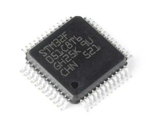
ARM 32-Bits Microprocessor STM32F051C6 Flash Heximal Restoration
ARM 32-Bits Microprocessor STM32F051C6 Flash Heximal Restoration can help engineer to extract source code from original mcu stm32f051c6 after break off the locked bits protection over microcomputer’s stm32f051c6 flash memory;
The high-speed external (HSE) clock can be supplied with a 4 to 32 MHz crystal/ceramic resonator oscillator. All the information given in this paragraph are based on design simulation results obtained with typical external components specified in below Table.
ARM 32-Bit mikroişlemci STM32F051C6 flash onaltılık geri yükleme, mühendisin mikrobilgisayarın STM32F051C6 flash belleği üzerindeki kilitli bit korumasını kestikten sonra orijinal MCU STM32F051C6’dan kaynak kodu çıkarmasına yardımcı olabilir;
In the application, the resonator and the load capacitors have to be placed as close as possible to the oscillator pins in order to minimize output distortion and startup stabilization time after recover stm32f051c4 microcontroller arm base chip memory binary. Refer to the crystal resonator manufacturer for more details on the resonator characteristics (frequency, package, accuracy).
- Resonator characteristics given by the crystal/ceramic resonator manufacturer.
- Guaranteed by design, not tested in production.
- This consumption level occurs during the first 2/3 of the tSU(HSE) startup time
- tSU(HSE) is the startup time measured from the moment it is enabled (by software) to a stabilized 8 MHz oscillation is reached. This value is measured for a standard crystal resonator and it can vary significantly with the crystal manufacturer
ARM Microcontroller STM32F051C4 Flash Binary Recovery
ARM Microcontroller STM32F051C4 Flash Binary Recovery means the embedded firmware of mcu stm32f051c4 will be copied from original chip stm32f051c4 which has been attacked by removing locked bit protection;
The wakeup times given in Table 32 are the latency between the event and the execution of the first user instruction. The device goes in low-power mode after the WFE (Wait For Event) instruction, in the case of a WFI (Wait For Interruption) instruction, 16 CPU cycles must be added to the following timings due to the interrupt latency in the Cortex M0 architecture.
The SYSCLK clock source setting is kept unchanged after wakeup from Sleep mode. During wakeup from Stop or Standby mode, SYSCLK takes the default setting: HSI 8 MHz in the process of recovering source code from ic mcu stm32f107rc.
ARM-Mikrocontroller STM32F051C4 Flash Binärwiederherstellung bedeutet, dass die eingebettete Firmware von mcu stm32f051c4 vom ursprünglichen Chip stm32f051c4 kopiert wird, der durch Entfernen des gesperrten Bitschutzes angegriffen wurde;
The wakeup source from Sleep and Stop mode is an EXTI line configured in event mode. The wakeup source from Standby mode is the WKUP1 pin (PA0).
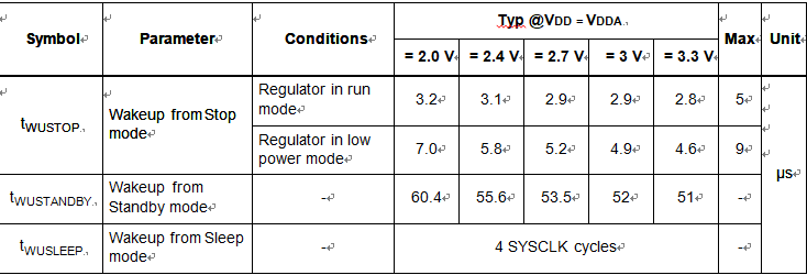
All timings are derived from tests performed under the ambient temperature and supply voltage conditions summarized in Table 20: General operating conditions.
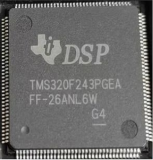
Attack Microcomputer TMS320F243PGE Flash Code Reading Protection
Attack Microcomputer TMS320F243PGE Flash Code Reading Protection needs to crack microcontroller tms320f243pge security fuse bit and then extract locked firmware from tms320f243pge flash memory;

Flash programming voltage pin and watchdog disable. This is the 5-V supply used for flash programming. Flash cannot be programmed if this pin is held at 0 V. This pin also works as a hardware watchdog disable, when VCCP/WDDIS = +5 V and bit 6 in WDCR is set to 1. Do not use a current-limiting resistor on this pin.
PLL oscillator input pin. Crystal input to PLL/clock source input to PLL. XTAL1/CLKIN is tied to one side of a reference crystal.
Crystal output. PLL oscillator output pin. XTAL2 is tied to one side of a reference crystal. This pin goes in the high-impedance state when EMU1/OFF is active low.
Clock output. This pin outputs either the CPU clock (CLKOUT) or the watchdog clock (WDCLK). The selection is made by the CLKSRC bit (bit 14) of the System Control and Status Register (SCSR) in the process of dsp microcontroller tms320f240pqe memory flash software recovery. This pin can be used as a GPIO if not used as a clock output pin.
External program space wait states. PSWS determines that between 0 to 7 wait states are applied to all reads and writes to off-chip program space address. The memory cycle can be further extended by using the READY signal. The READY signal does not override the wait states generated by PSWS. These bits are set to 1 (active) by reset (RS).
Angriffsmikrocomputer TMS320F243PGE Flash Code Leseschutz muss Mikrocontroller tms320f243pge Sicherheits Sicherungsbit knacken und dann gesperrte Firmware aus tms320f243pge Flash Speicher extrahieren;
External data space wait states. DSWS determines that between 0 to 7 wait states are applied to all reads and writes to off-chip data space. The memory cycle can be further extended by using the READY signal after decoding tms320f241fn dsp mcu program. The READY signal does not override the wait states generated by DSWS. These bits are set to 1 (active) by reset (RS).
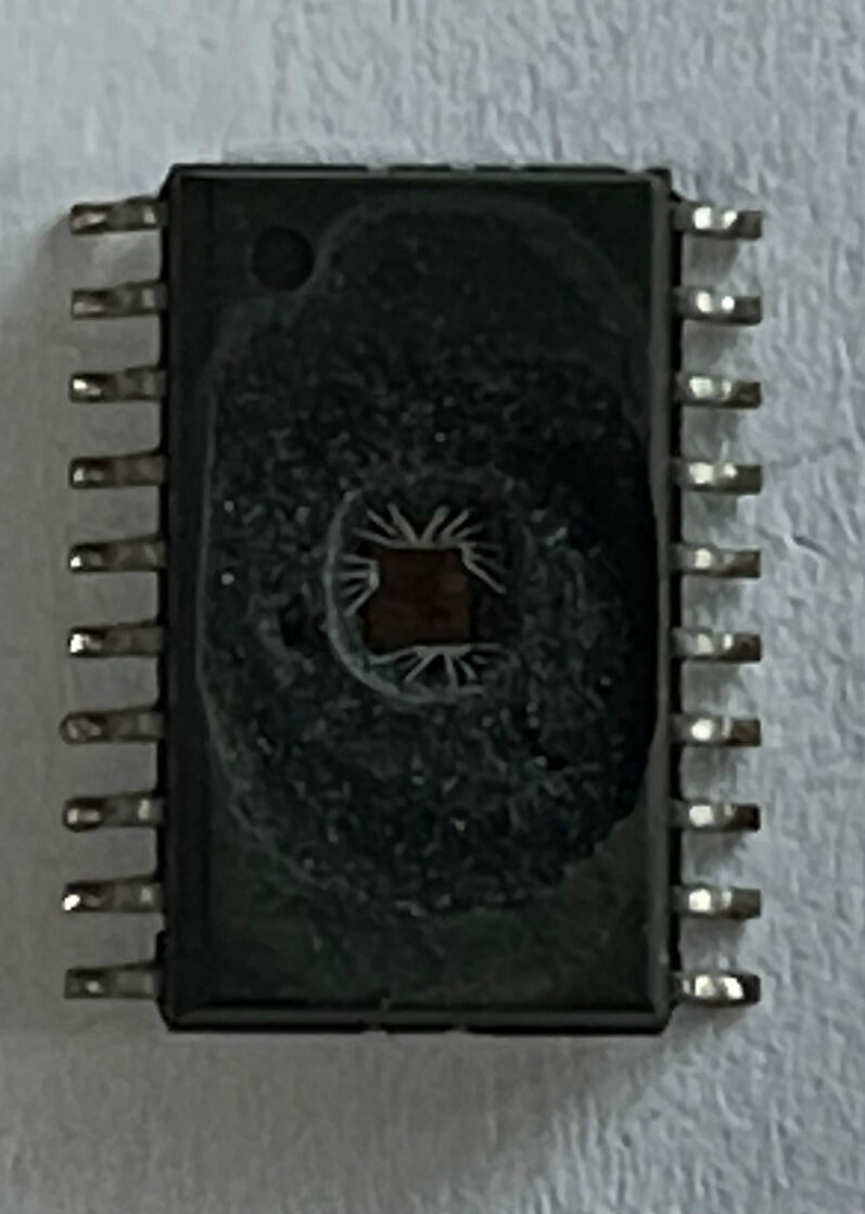
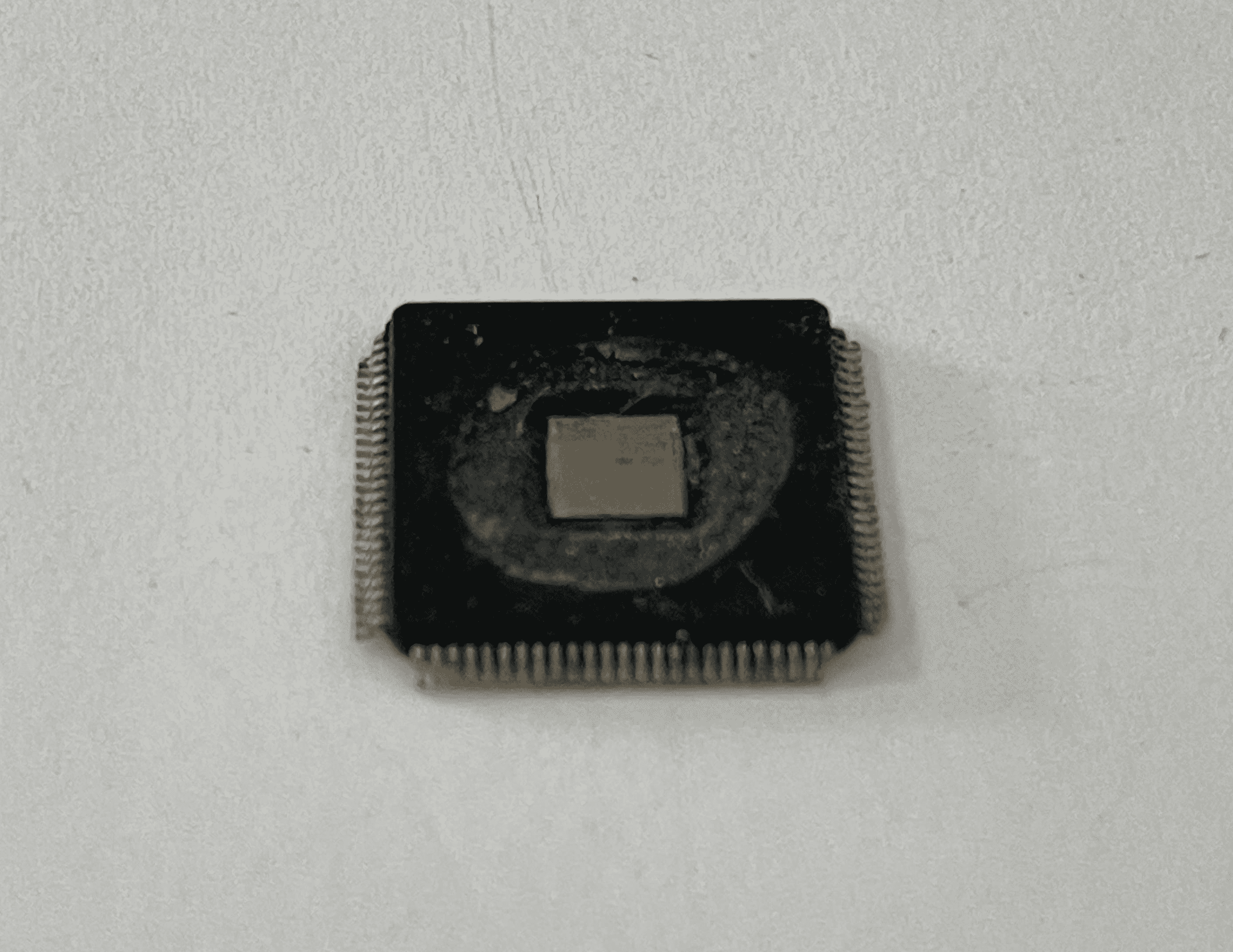
Break DSP MCU TMS320F243FN Flash Memory
Break DSP MCU TMS320F243FN Flash Memory locked bit protection is a process to crack microcontroller tms320f243fn tamper resistance system, and then readout embedded binary from microprocessor tms320f243fn flash memory;
PLL oscillator input pin. Crystal input to PLL/clock source input to PLL. XTAL1/CLKIN is tied to one side of a reference crystal.
Crystal output. PLL oscillator output pin. XTAL2 is tied to one side of a reference crystal. This pin goes in the high-impedance state when EMU1/OFF is active low.
Clock output. This pin outputs either the CPU clock (CLKOUT) or the watchdog clock (WDCLK). The selection is made by the CLKSRC bit (bit 14) of the System Control and Status Register (SCSR). This pin can be used as a GPIO if not used as a clock output pin.
разбить DSP MCU TMS320F243FN блокировка битовой защиты флэш-памяти – это процесс взлома системы защиты от несанкционированного доступа микроконтроллера TMS320F243FN, а затем считывания встроенного двоичного файла с флэш-памяти микропроцессора TMS320F243fn;
JTAG test clock with internal pullup, JTAG test data input (TDI) with internal pullup. TDI is clocked into the selected register (instruction or data) on a rising edge of TCK in the process of dsp microprocessor tms320f240pga flash memory decryption. JTAG scan out, test data output (TDO). The contents of the selected register (instruction or data) is shifted out of TDO on the falling edge of TCK.
JTAG test-mode select (TMS) with internal pullup. This serial control input is clocked into the TAP controller on the rising edge of TCK.
TI IC MCU TMS320F241FNA Flash Program Decoding
TI IC MCU TMS320F241FNA Flash Program Decoding will provide end user the embedded firmware extracted from flash memory of microcontroller tms320f241fna, after unlock heximal file from new tms320f241fna processor;
Bus request, global memory strobe. BR is asserted during access of external global data memory space. BR can be used to extend the data memory address space by up to 32K words. BR goes in the high-impedance state during reset, power down, and when EMU1/OFF is active low.
Visibility clock. Same as CLKOUT, but timing is aligned for external buses in visibility mode to recover mcu tms320f240fp flash software.
Active high to enable external interface signals. If pulled low, the F243 behaves like an F241—i.e., it has no external memory and generates an illegal address if any of the three external spaces are accessed (IS, DS, PS asserted). This pin has an internal pulldown.
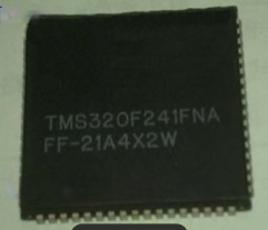
Декодирование программы флэш-памяти TI IC MCU TMS320F241FNA предоставит конечному пользователю встроенную прошивку, извлеченную из флэш-памяти микроконтроллера TMS320F241FNA, после разблокировки шестнадцатеричного файла с нового процессора TMS320F241FNA;
This pin is active (low) whenever the external databus is driving as an output during visibility mode. Can be used by external decode logic to prevent data bus contention while running in visibility mode.
External flag output (latched software-programmable signal). XF is a general-purpose output pin. It is set/reset by the SETC XF/CLRC XF instruction in the process of dsp microprocessor tms320f240pqa flash memory decryption. This pin is configured as an external flag output by all device resets. It can be used as a GPIO, if not used as XF.
Branch control input. BIO is polled by the BCND pma,BIO instruction. If BIO is low, a branch is executed. If BIO is not used, it should be pulled high. This pin is configured as a branch control input by all device resets. It can be used as a GPIO, if not used as a branch control input.
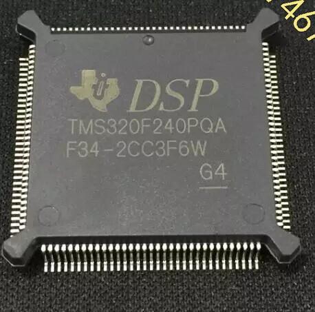
Decrypt DSP Microprocessor TMS320F240PQA Flash Memory
Decrypt DSP Microprocessor TMS320F240PQA Flash Memory protection needs to unlock dsp mcu tms320f240pqa tamper resistance system over its flash memory, and then extract source code from dsp controller tms320f240pqa flash memory;
Write enable strobe. The falling edge of WE indicates that the device is driving the external data bus (D15 −D0). WE is active on all external program, data, and I/O writes. WE goes in the high-impedance state when EMU1/OFF is active low.
Read enable strobe. Read-select indicates an active, external read cycle. RD is active on all external program, data, and I / O reads for breaking tms320f240 mcu locked flash memory. RD goes into the high-impedance state when EMU1/OFF is active low.
расшифровать микропроцессор DSP TMS320F240PQA Защита флэш-памяти должна разблокировать систему защиты от несанкционированного доступа DSP MCU TMS320F240PQA через свою флэш-память, а затем извлечь исходный код из флэш-памяти контроллера DSP TMS320F240PQA
Read/write signal. R/W indicates transfer direction during communication to an external device. It is normally in read mode (high), unless low level is asserted for performing a write operation. It is placed in the high-impedance state when EMU1/OFF is active low and during power down.
External memory access strobe. STRB is always high unless asserted low to indicate an external bus cycle. STRB is active for all off-chip accesses in the process of dsp microcomputer tms320f240pga flash software recovery. It is placed in the high-impedance state during power down, and when EMU1/OFF is active low.