 Copy Infineon Locked MCU MB90F342CAPFR-G Flash Heximal
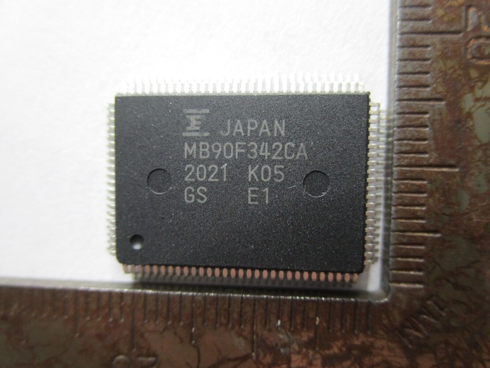
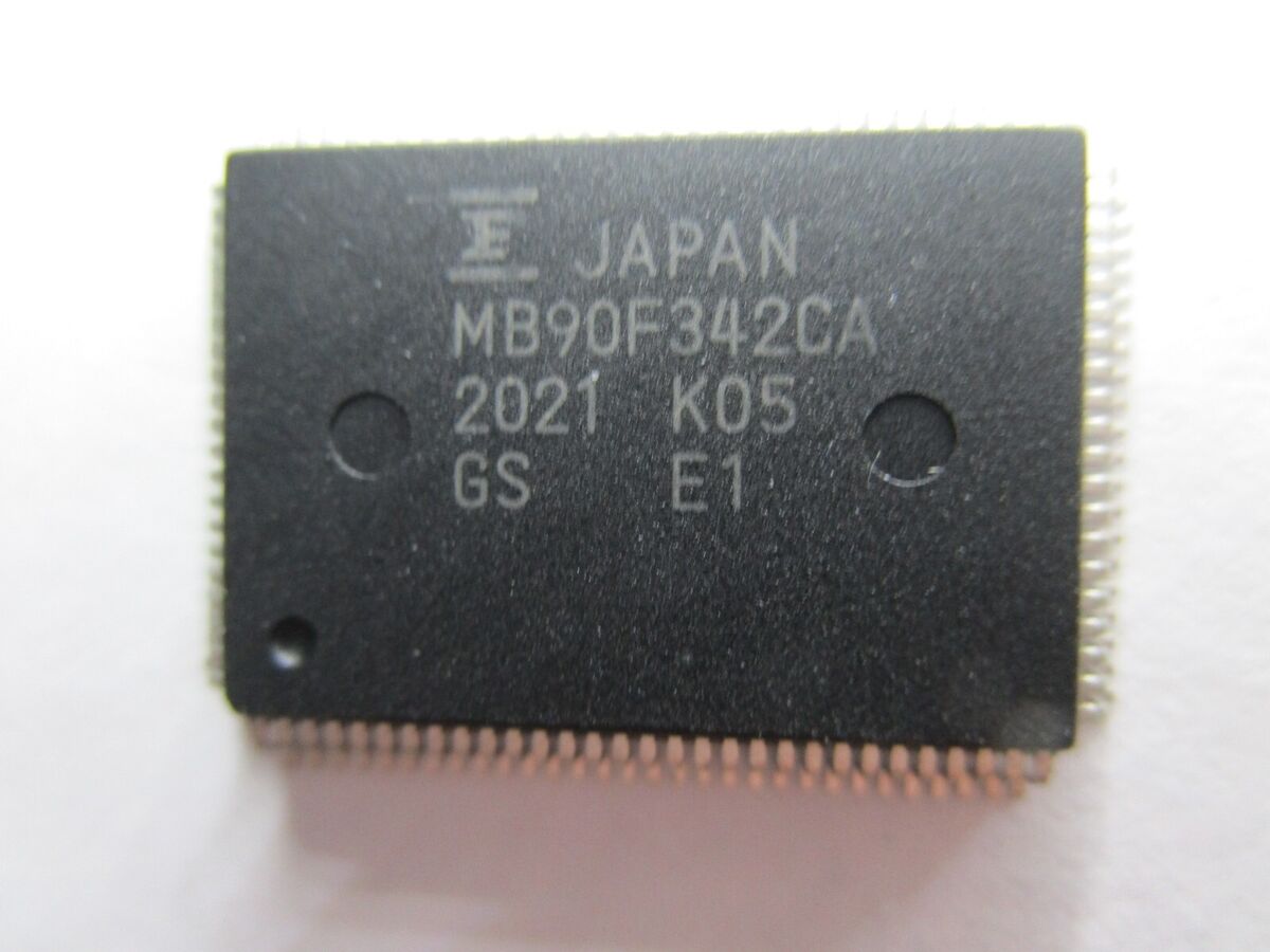
Copy Infineon Locked MCU MB90F342CAPFR-G Flash Heximal to new microcontroller, unlock fujitsu MB90F342CAP secured microcontroller flash memory and clone MB90F342E flash firmware to new microprocessor;
Copy Infineon Locked MCU MB90F342CAPFR-G Flash Heximal to new microcontroller, unlock fujitsu MB90F342CAP secured microcontroller flash memory and clone MB90F342E flash firmware to new microprocessor;
The recommended operating conditions are required in order to ensure the normal operation of the semiconductor device. All of the device’s electrical characteristics are warranted when the device is operated within these ranges.
Always use semiconductor devices within their recommended operating condition ranges. Operation outside these ranges may adversely affect reliability and could result in device failure.
Copiez le micrologiciel intégré flash INFINEON verrouillé MCU MB90F342CAPFR-G des données heximales ou du fichier binaire sur le nouveau microcontrôleur, déverrouillez la mémoire flash sécurisée du microprocesseur FUJITSU MB90F342CAP et répliquez le programme MB90F342E sur une nouvelle unité clonée par microprocesseur ;
No warranty is made with respect to uses, operating conditions, or combinations not represented on the data sheet. Users considering application outside the listed conditions are advised to contact their FUJITSU representatives beforehand.
The oscillation time of the oscillator is the time it takes for the amplitude of the oscillations to reach 90%. For crystal oscillators, this time is between several ms and several tens of ms to reverse engineering MB90F345CA microcontroller flash memory, for ceramic oscillators the time is between several hundred ms and several ms, and for an external clock, the time is 0 ms.
Kopieren Sie die von INFINEON gesperrte MCU MB90F342CAPFR-G-Flash-eingebettete Firmware von Heximaldaten oder Binärdateien auf den neuen Mikrocontroller, entsperren Sie den FUJITSU MB90F342CAP-gesicherten Mikroprozessor-Flash-Speicher und replizieren Sie das MB90F342E-Programm auf die neue geklonte Mikroprozessoreinheit;
Resolution : Analog variation that is recognized by the A/D converter.
Non linearity error
Differential linearity error : The deviation between the actual conversion characteristics and a line that joins the
zero-transition line ( “00 0000 0000” ¬ ® “00 0000 0001” ) to the full-scale transition line
( “11 1111 1110” ¬ ® “11 1111 1111” ) . : Deviation of input voltage, which is required for changing output code by 1 LSB, from an ideal value.
Use the device with external circuits of the following output impedance for analog inputs :
Recommended output impedance of external circuits are : Approx. 1.5 kL or lower (4.0 V £ AVCC £ 5.5 V,
sampling period = 0.5 ms)
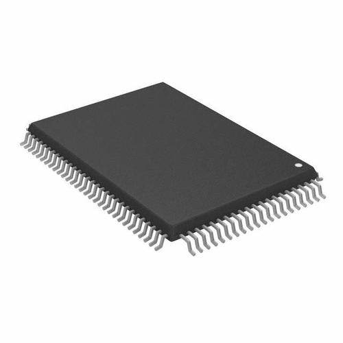
Restoring Infineon MB90F342APFV-G MCU Flash Firmware
Restoring Infineon MB90F342APFV-G MCU Flash Firmware needs to unlock Fujitsu MB90F342ES microcontroller secured IC flash memory and then dump flash memory binary to new microcontroller MB90F342APFV;
Restoring Infineon MB90F342APFV-G MCU Flash Firmware needs to unlock Fujitsu MB90F342ES microcontroller secured IC flash memory and then dump flash memory binary to new microcontroller MB90F342APFV;
This parameter is based on VSS = AVSS = 0 V
*2: Set AVCC and VCC to the same voltage. Make sure that AVCC does not exceed VCC and that the voltage at the analog inputs does not exceed AVCC when the power is switched on.
*3: VI and VO should not exceed VCC + 0.3 V. VI should not exceed the specified ratings. However if the maximum current to/from an input is limited by some means with external components, the ICLAMP rating supersedes the VI rating.
*4: Applicable to pins: P00 to P07, P10 to P17, P20 to P27, P30 to P37, P40 to P47, P50 to P57, P60 to P67, P70 to P77, P80 to P87, P90 to P97, PA0, PA1
*5: · Applicable to pins: P00 to P07, P10 to P17, P20 to P27, P30 to P37, P40 to P47,
відновлення вбудованої прошивки флеш-пам’яті INFINEON MB90F342APFV-G із заблокованим MCU потрібно зламати флеш-пам’ять мікроконтролера FUJITSU MB90F342ES, а потім витягти двійковий код або шістнадцяткові дані на новий мікропроцесор MB90F342APFV
P50 to P57 (Evaluation device : P50 to P55) , P60 to P67, P70 to P77, P80 to P87, P90 to P97, PA0 to PA1
- Use within recommended operating
- Use with DC voltage (current)
- The +B signal should always be applied by using a limiting resistance placed between the +B signal and the
- The value of the limiting resistance should be set so that when the +B signal is applied, the input current to the microcontroller pin does not exceed the rated value, either instantaneously or for prolonged
- Note that when the microcontroller drive current is low, such as in the power saving modes, the +B input
Az INFINEON MB90F342APFV-G zárolt MCU flash beágyazott firmware-ének helyreállításához fel kell törnie a FUJITSU-t MB90F342ES mikrokontrollerrel biztosított IC flash memóriát, majd bináris kódot vagy heximalis adatokat kell kinyernie az új mikroprocesszorba MB90F342APFV
potential may pass through the protective diode and increase the potential at the VCC pin when restoring secured fujitsu MCU MB90F345CAP heximal code, and this may affect other devices.
- Note that if a +B signal is input when the microcontroller power supply is off (not fixed at 0 V) , the power supply is provided from the pins, so that incomplete operation may result.
- Note that if the +B input is applied during power-on, the power supply is provided from the pins and the resulting supply voltage may not be sufficient to operate the power-on reset.
- Care must be taken not to leave the +B input pin
Readout Renesas R7F7010124AFP Locked MCU Flash Content
Readout Renesas R7F7010124AFP Locked MCU Flash Content needs to firstly crack R7F7010124AFP secured microcontroller fuse bit and then copy flash program in the format of binary to new microprocessor R7F7010124afp;
Readout Renesas R7F7010124AFP Locked MCU Flash Content needs to firstly crack R7F7010124AFP secured microcontroller fuse bit and then copy flash program in the format of binary to new microprocessor R7F7010124afp;
A strong electric field, when exposed to a MOS device, can cause destruction of the gate oxide and ultimately degrade the device operation. Steps must be taken to stop generation of static electricity as much as possible, and quickly dissipate it when it has occurred. Environmental control must be adequate.
When it is dry, a humidifier should be used. It is recommended to avoid using insulators that easily build up static electricity. Semiconductor devices must be stored and transported in an anti-static container when copying renesas microcontroller M306NKFH flash program, static shielding bag or conductive material. All test and measurement tools including work benches and floors should be grounded.
kiolvasás A RENESAS védő R7F7010124AFP zárolt MCU flash tartalomnak először fel kell törnie R7F7010124AFP biztonságos mikrovezérlő biztosítékbitjét, majd bináris forráskód vagy hexaximális adatok formájában flash programot kell másolnia az új mikroprocesszorra R7F7010124AFP
The operator should be grounded using a wrist strap. Semiconductor devices must not be touched with bare hands. Similar precautions need to be taken for PW boards with mounted semiconductor devices.
Power-on does not necessarily define the initial status of a MOS device. Immediately after the power source is turned ON, devices with reset functions have not yet been initialized when reading renesas microprocessor R5F212AASD flash binary file. Hence, power-on does not guarantee output pin levels, I/O settings or contents of registers. A device is not initialized until the reset signal is received. A reset operation must be executed immediately after power-on for devices with reset functions.
зчитування захисного R7F7010124AFP заблокованого вмісту мікроконтролера потрібно спочатку зламати R7F7010124AFP захищений біт запобіжника мікроконтролера, а потім скопіювати програму флеш-пам’яті у форматі двійкового вихідного коду або шістнадцяткових даних на новий мікропроцесор R7F7010124AFP
Recover RH850 R7F7010303AFP Microcontroller Flash Heximal
Recover RH850 R7F7010303AFP Microcontroller Flash Heximal needs to crack R7F7010303AFP renesas locked MCU protection and then pull the embedded firmware out from microprocessor R7F7010303afp flash memory;
Recover RH850 R7F7010303AFP Microcontroller Flash Heximal needs to crack R7F7010303AFP renesas locked MCU protection and then pull the embedded firmware out from microprocessor R7F7010303afp flash memory;
Waveform distortion due to input noise or a reflected wave may cause malfunction. If the input of the CMOS device stays in the area between VIL (MAX) and VIH (MIN) due to noise, etc., the device may malfunction. Take care to prevent chattering noise from entering the device when the input level is fixed when cracking renesas microcontroller R5F563NFDDF flash memory, and also in the transition period when the input level passes through the area between VIL (MAX) and VIH (MIN).
recuperare il programma flash del microcontroller bloccato RH850 R7F7010303AFP nel formato di file binario o dati esimali deve crackare la protezione MCU RENESAS protetta da R7F7010303AFP e quindi estrarre il firmware incorporato dalla memoria flash crittografata del microprocessore RENESAS R7F7010303afp;
Unconnected CMOS device inputs can be cause of malfunction. If an input pin is unconnected, it is possible that an internal input level may be generated due to noise, etc., causing malfunction. CMOS devices behave differently than Bipolar or NMOS devices.
Input levels of CMOS devices must be fixed high or low by using pull-up or pull-down circuitry. Each unused pin should be connected to power supply or GND via a resistor if there is a possibility that it will be an output pin to attack renesas R5F5111FAD mcu flash memory. All handling related to unused pins must be judged separately for each device and according to related specifications governing the device.
recuperați programul flash de microcontroler blocat RH850 R7F7010303AFP în format de fișier binar sau de date heximale trebuie să spargă protecția MCU RENESAS securizată R7F7010303AFP și apoi scoateți firmware-ul încorporat din memoria flash criptată a microprocesorului RENESAS R7F7010303afp;
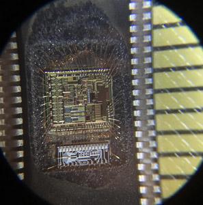
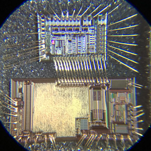
Reverse MB90F345CAPMC-GS Infineon Microcontroller Memory
Reverse MB90F345CAPMC-GS Infineon Microcontroller Memory and then clone locked microprocessor MB90F345CAP embedded firmware out from its flash memory, after attacking MCU MB90F345CAPMC protective system;
Reverse MB90F345CAPMC-GS Infineon Microcontroller Memory and then clone locked microprocessor MB90F345CAP embedded firmware out from its flash memory, after attacking MCU MB90F345CAPMC protective system;
Make sure to turn on the A/D converter power supply (AVCC, AVRH, AVRL) and analog inputs (AN0 to AN23) after turning-on the digital power supply (VCC).
Turn-off the digital power after turning off the A/D converter supply and analog inputs. In this case, make sure that the voltage does not exceed AVRH or AVCC (turning on/off the analog and digital power supplies simulta- neously is acceptable).
reverse engineering MB90F345CA INFENION sistema di protezione della memoria del microcontrollore protetto e quindi estrazione del firmware incorporato del microprocessore bloccato MB90F345CAP dalla sua memoria flash come formato di codice binario o dati essimali, dopo aver attaccato la resistenza alla manomissione MCU crittografata INFENION MB90F345CA;
The X0, X1 pins and X0A, X1A pins may be possible causes of abnormal operation. Make sure to provide bypass capacitors via the shortest distance from X0, X1 pins and X0A, X1A pins, crystal oscillator (or ceramic oscillator) and ground lines, and make sure, to the utmost effort, that the oscillation circuit lines do not cross the lines of other circuits. It is highly recommended to provide a printed circuit board art work surrounding X0, X1 pins and X0A, X1A pins with a ground area for stabilizing the operation.
For each of the mass-production products, request an oscillator evaluation from the manufacturer of the oscillator you are using. The MB90340E Series does not support internal pull-up/down resistors (except for the pull-up resistors built into ports 0 to 3). Use external components where needed. If you do not connect pins X0A and X1A to an oscillator, use pull-down handling on the X0A pin, and leave the X1A pin open.
inginerie inversă MB90F345CA INFENION securizat sistemul de protecție a memoriei microcontrolerului și apoi extrageți microprocesorul blocat MB90F345CAP firmware încorporat din memoria flash ca format de cod binar sau date heximale, după ce a atacat MCU criptat INFENION MB90F345CA rezistență la falsificare;
If PLL clock mode is selected, the microcontroller attempt to be working with the self-oscillating circuit even when there is no external oscillator or the external clock input is stopped. Performance of this operation, however, cannot be guaranteed. To prevent the internal regulator circuit from malfunctioning, set the voltage rise time during power-on to 50 ms or more (0.2 V to 2.7 V)
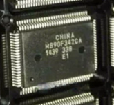
Fujitsu Secured MCU MB90F345CAPF-G Heximal Code Restoration
Fujitsu Secured MCU MB90F345CAPF-G Heximal Code Restoration starts from attacking IC processor MB90F345 protection and readout microprocessor MB90F345 flash memory program;
Fujitsu Secured MCU MB90F345CAPF-G Heximal Code Restoration starts from attacking IC processor MB90F345 protection and readout microprocessor MB90F345 flash memory program;
CMOS IC chips may suffer latch-up under the following conditions:
A voltage higher than VCC or lower than VSS is applied to an input or output
A voltage higher than the rated voltage is applied between VCC and VSS
The AVCC power supply is applied before the VCC
Latch-up may increase the power supply current drastically, causing thermal damage to the device.
For the same reason, also be careful not to let the analog power-supply voltage (AVCC, AVRH) exceed the digital power-supply voltage.
Leaving unused input pins open may result in misbehavior or latch-up and possible permanent damage to the device. Therefore they must be pulled up or pulled down through resistors. In this case those resistors should be more than 2 kL .
Unused bidirectional pins should be set to the output state and can be left open, or the input state with the above described connection.
Restaurarea codului sursă binar sau heximal al MCU securizat FUJITSU MB90F345CAPF-G pornește de la microprocesorul de protecție împotriva fisurilor MB90F345 bit de siguranță și citirea blocată a microcontrolerului MB90F345 firmware încorporat din memoria flash
If there are multiple VCC and VSS pins, that are designed to be set to the same potential are connected the inside of the device to prevent malfunctions such as latch-up.
To reduce unnecessary radiation, prevent malfunctioning of the strobe signal due to the rise of ground level, and observe the standard for total output current, be sure to connect the VCC and VSS pins to the power supply and ground externally. Connect VCC and VSS pins to the device from the current supply source at a low impedance.
MCU protetto MB90F345CAPF-G il ripristino del codice sorgente binario o esadecimale inizia dal microprocessore protettivo contro le crepe Bit del fusibile di protezione MB90F345 e lettura bloccata Microcontroller MB90F345 firmware incorporato dalla sua memoria flash
Connect the mode pins directly to VCC or VSS pins. To prevent the device unintentionally entering test mode due to noise, lay out the printed circuit board so as to minimize the distance from the mode pins to VCC or VSS pins and to provide a low-impedance connection.
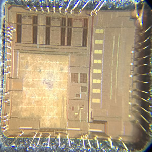
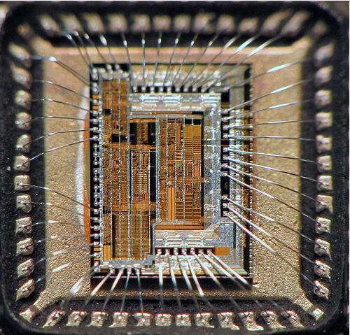
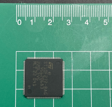
Reverse Engineering ST10F272M-4QR3 Encrypted Microprocessor Memory
Reverse Engineering ST10F272M-4QR3 Encrypted Microprocessor Memory can help designer to recover embedded flash content of microcontroller st10f272m-4qr3 and clone flash program in the format of binary or heximal to new MCU ST10F272M-4QR3;
Reverse Engineering ST10F272M-4QR3 Encrypted Microprocessor Memory can help designer to recover embedded flash content of microcontroller st10f272m-4qr3 and clone flash program in the format of binary or heximal to new MCU ST10F272M-4QR3;
Output transition is not programmable.
CAN module is enhanced: ST10F273 implements two C-CAN modules, so the programming model is slightly different. Besides, the possibility to map in parallel the two CAN modules is added (on P4.5/P4.6).
On-chip main oscillator input frequency range has been reshaped, reducing it from 1 to 25 MHz down to 4 to 12 MHz. This is a low power oscillator amplifier, that allows a power consumption reduction when Real Time Clock is running in Power down mode, using as reference the on-chip main oscillator clock. When this on-chip amplifier is used as reference for Real Time Clock module, the Power-down consumption is dominated by the consumption of the oscillator amplifier itself.
зворотне проектування ST10F272M зашифрована захисна система мікропроцесора для зчитування вбудованого мікропрограмного забезпечення з флеш-пам’яті може допомогти розробнику відновити флеш-вміст двійкового файлу та шістнадцяткових даних з мікроконтролера ST10F272M
A second on-chip oscillator amplifier circuit (32 kHz) is implemented for low power modes: it can be used to provide the reference to the Real Time Clock counter (either in Power down or Stand-by mode). Pin XTAL3 and XTAL4 replace a couple of VDD/VSS pins of ST10F272M-4QR3.
visszafejtés Az ST10F272M titkosított mikroprocesszoros védelmi rendszer a beágyazott firmware flash memóriából történő kiolvasásához segíthet a tervezőnek a bináris fájlok flash tartalmának és a heximális adatoknak az ST10F272M mikrokontrollerről történő helyreállításában
8-bit bidirectional I/O port, bit-wise programmable for input or output via direction bit. Programming an I/O pin as input forces the corresponding output driver to high impedance state. Port 6 outputs can be configured as push-pull or open drain drivers. The input threshold of Port 6 is selectable (TTL or CMOS). The following Port 6 pins have alternate functions:
External access enable pin.
A low level applied to this pin during and after Reset forces the ST10F273 to start the program from the external memory space. A high level forces ST10F273 to start in the internal memory space. This pin is also used (when Stand-by mode is entered, that is ST10F273 under reset and main VDD turned off) to bias the 32 kHz oscillator amplifier circuit and to provide a reference voltage for the low-power embedded voltage regulator which generates the internal 1.8V supply for the RTC module (when not disabled) and to retain data inside the Stand-by portion of the XRAM (16Kbyte).
engenharia reversa O sistema de proteção do microprocessador criptografado ST10F272M para ler o firmware incorporado da memória flash pode ajudar o designer a recuperar o conteúdo flash do arquivo binário e dados heximais do microcontrolador ST10F272M
It can range from 4.5 to 5.5V (6V for a reduced amount of time during the device life, 4.0V when RTC and 32 kHz on-chip oscillator amplifier are turned off). In running mode, this pin can be tied low during reset without affecting 32 kHz oscillator, RTC and XRAM activities, since the presence of a stable VDD guarantees the proper biasing of all those modules.
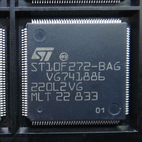
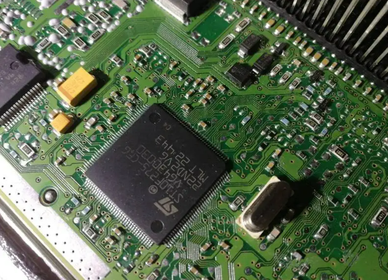
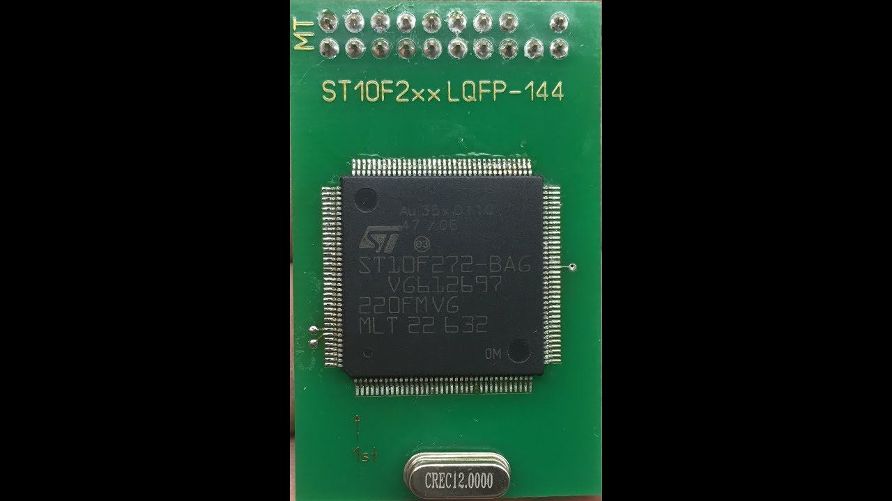
STMicroelectronics ST10F272M-4T3 Locked MCU Flash Content Recovery
STMicroelectronics ST10F272M-4T3 Locked MCU Flash Content Recovery is a process to crack ST10F272M-4T3 secured microcontroller protective fuse bit and copy the embedded software to new microprocessor ST10F272M-4T3;
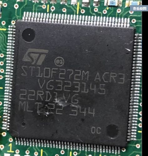
STMicroelectronics ST10F272M-4T3 Locked MCU Flash Content Recovery is a process to crack ST10F272M-4T3 secured microcontroller protective fuse bit and copy the embedded software to new microprocessor ST10F272M-4T3;
CLKOUT function can output either the CPU clock (like in ST10F272M-4T3) or a software programmable prescaled value of the CPU clock. On-chip RAM memory and FLASH size have been increased. PLL multiplication factors have been adapted to new frequency range. A/D Converter is not fully compatible versus ST10F272M-4T3 (timing and programming model). Formula for the conversion time is still valid, while the sampling phase programming model is different.
STMicroelectronics ST10F272M locked MCU flash programme recovery – це процес зламу ST10F272M захищеного біта захисного запобіжника мікроконтролера та зчитування вбудованого мікропрограмного забезпечення двійкового коду або шістнадцяткового файлу з оригінальної головної мікросхеми, а потім копіювання вихідного коду на новий мікропроцесор ST10F272M
Besides, additional 8 channels are available on P1L pins as alternate function: The accuracy reachable with these extra channels is reduced with respect to the standard Port5 channels. External Memory bus is affected by limitations on maximum speed and maximum capacitance load: ST10F272m is not able to address an external memory at 64 MHz with 0 wait states in the process of cloning flash memory of locked mcu st10f272m.
A recuperação do programa flash MCU bloqueado ST10F272M da STMicroelectronics é um processo para quebrar o bit de fusível de proteção do microcontrolador protegido ST10F272M e ler o firmware incorporado do código binário ou arquivo heximal do chip mestre original e depois copiar o código-fonte para o novo microprocessador ST10F272M
XPERCON register bit mapping modified according to new peripherals implementation (not fully compatible with ST10F272m). Bondout chip for emulation (ST10R201) cannot achieve more than 50MHz at room temperature (so no real time emulation possible at maximum speed).
Az STMicroelectronics ST10F272M zárolt MCU flash program helyreállítása egy folyamat az ST10F272M biztonságos mikrokontroller védőbiztosíték bitjének feltörésére és a bináris kód vagy heximális fájl beágyazott firmware-ének kiolvasására az eredeti master chipről, majd a forráskód átmásolására az új ST10F272M mikroprocesszorra
Input section characteristics are different. The threshold programmability is extended to all port pins (additional XPICON register); it is possible to select standard TTL (with up to 400mV of hysteresis) and standard CMOS (with up to 750mV of hysteresis).
Reverse Engineer ARM STM32F105V8 Microcomputer Program
Reverse Engineer ARM STM32F105V8 Microcomputer Program can help engineer to extract source code of heximal file from secured microprocessor stm32f105v8, and then copy flash binary software to new stm32f105v8 mcu;
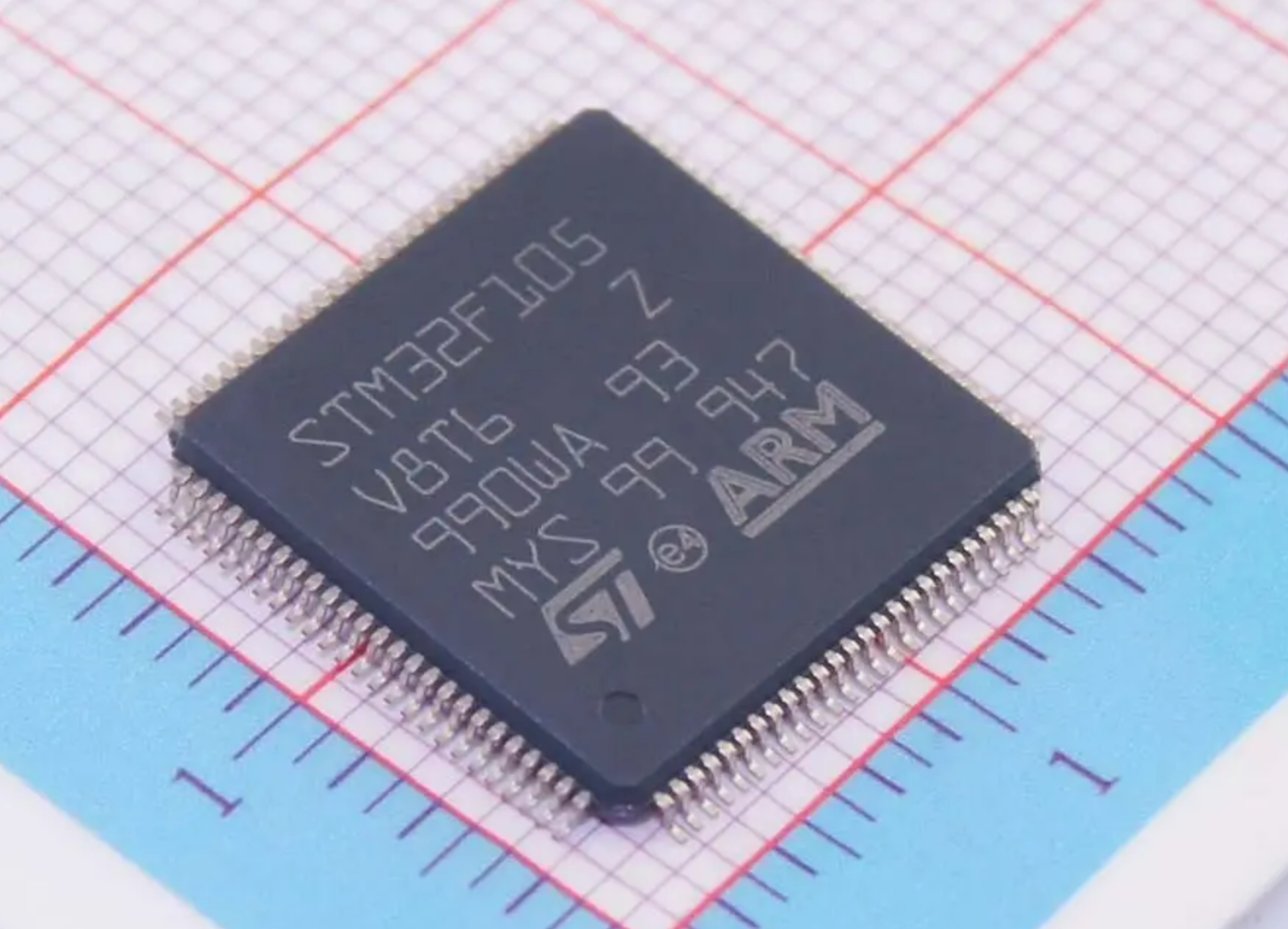
Reverse Engineer ARM STM32F105V8 Microcomputer Program can help engineer to extract source code of heximal file from secured microprocessor stm32f105v8, and then copy flash binary software to new stm32f105v8 mcu
The independent watchdog is based on a 12-bit downcounter and 8-bit prescaler. It is clocked from an independent 40 kHz internal RC and as it operates independently of the main clock, it can operate in Stop and Standby modes. It can be used either as a watchdog to reset the device when a problem occurs after replicating stm32f105r8 mcu chip embedded flash program, or as a free-running timer for application timeout management. It is hardware- or software-configurable through the option bytes. The counter can be frozen in debug mode.
The window watchdog is based on a 7-bit downcounter that can be set as free-running. It can be used as a watchdog to reset the device when a problem occurs. It is clocked from the main clock. It has an early warning interrupt capability and the counter can be frozen in debug mode.
crack locked microprocessor STM32F105V8 fuse bit and extract embedded source code from mcu chip STM32F105V8
This timer is dedicated for OS, but can be used also as a standard downcounter. It features:
- A 24-bit downcounter
- Autoreload capability
- Maskable system interrupt generation when the counter reaches 0
- Programmable clock source
Up to two I²C bus interfaces can operate in multimaster and slave modes. They can support standard and fast modes. They support dual slave addressing (7-bit only) and both 7/10-bit addressing in master mode to decrypt mcu chip stm32f105vc secured memory binary program. A hardware CRC generation/verification is embedded. They can be served by DMA and they support SM Bus 2.0/PM Bus.
descifrar el microcontrolador del brazo STM32F105V8 y extraer el firmware integrado heximal de la memoria flash
Reverse Encrypted STM32F103VB Microprocessor Protection
Reverse Encrypted STM32F103VB Microprocessor Protection and clone stm32f103vb locked mcu flash heximal file, copy flash memory firmware to arm microcontroller stm32f103vb;
Reverse Encrypted STM32F103VB Microprocessor Protection and clone stm32f103vb locked mcu flash heximal file, copy flash memory firmware to arm microcontroller stm32f103vb
The advanced-control timer (TIM1) can be seen as a three-phase PWM multiplexed on 6 channels. It has complementary PWM outputs with programmable inserted dead-times. It can also be seen as a complete general-purpose timer. The 4 independent channels can be used for
- Input capture
- Output compare
- PWM generation (edge- or center-aligned modes)
- One-pulse mode output
If configured as a general-purpose 16-bit timer, it has the same features as the TIMx timer. If configured as the 16-bit PWM generator, it has full modulation capability (0-100%).
In debug mode, the advanced-control timer counter can be frozen and the PWM outputs disabled to turn off any power switch driven by these outputs.
Many features are shared with those of the general-purpose TIM timers which have the same architecture. The advanced-control timer can therefore work together with the TIM timers via the Timer Link feature for synchronization or event chaining to recover stm32f103c6 locked mcu flash full content.
clone STMicroelectronics-STM32F103VB microprocessor flash memory content and copy embedded heximal file and binary program to new mcu chip STMicroelectronics-STM32F103VB
There are up to three synchronizable general-purpose timers embedded in the STM32F103xx performance line devices. These timers are based on a 16-bit auto-reload up/down counter, a 16-bit prescaler and feature four independent channels each for input capture/output compare, PWM or one-pulse mode output. This gives up to 12 input captures/output compares/PWMs on the largest packages.
Desbloquee el microcontrolador de brazo MCU STM32F105VBT6 y lea el firmware integrado heximal de la memoria flash
The general-purpose timers can work together with the advanced-control timer via the Timer Link feature for synchronization or event chaining. Their counter can be frozen in debug mode. Any of the general-purpose timers can be used to generate PWM outputs. They all have independent DMA request generation when recovering arm microprocessor stm32f103cb flash program.
These timers are capable of handling quadrature (incremental) encoder signals and the digital outputs from one to three Hall-effect sensors.