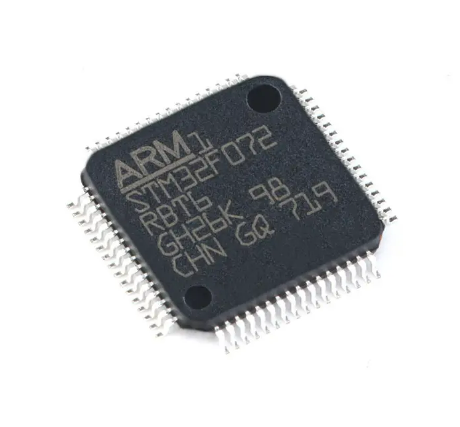
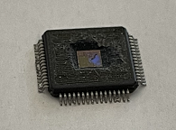
Recover ARM STM32F078CB Microprocessor Flash Firmware
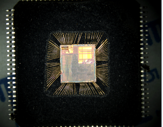
Recover ARM STM32F078CB Microprocessor Flash Firmware from its secured flash memory, the mcu stm32f078cb will be cracked by focus ion beam to disable its protection and then readout embedded heximal file from stm32f078cb microcomputer’s memory;
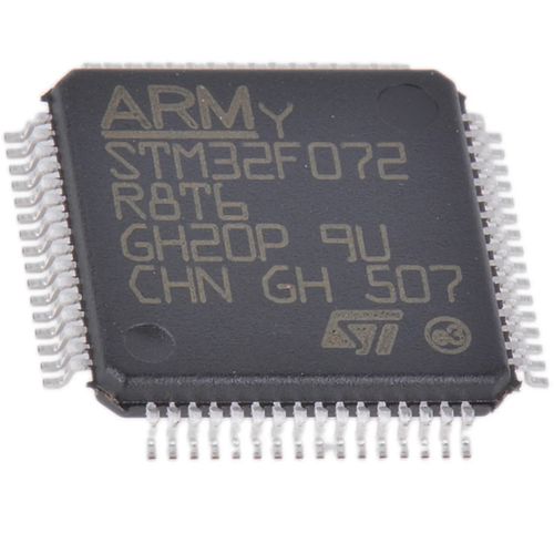
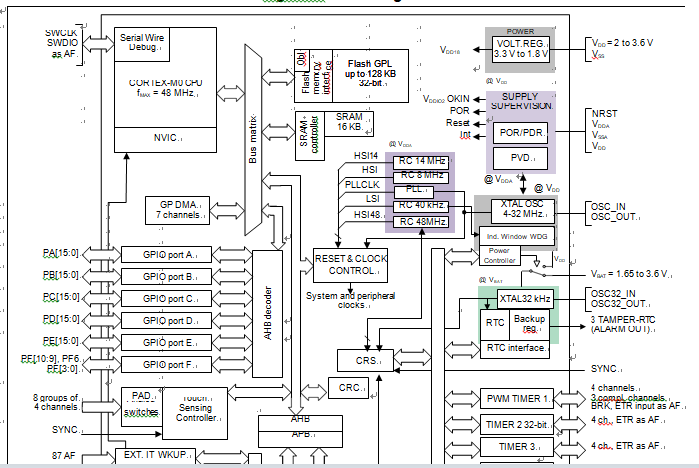
The STM32F078CB/RB/VB microcontrollers incorporate the high-performance Arm®Cortex®-M0 32-bit RISC core operating at up to 48 MHz frequency, high-speed
embedded memories (128 Kbytes of Flash memory and 16 Kbytes of SRAM), and an extensive range of enhanced peripherals and I/Os. All devices offer standard communication interfaces (two I2Cs, two SPI/I2S, one HDMI CEC and four USARTs), one USB Full-speed device (crystal-less), one 12-bit ADC, one 12-bit DAC with two channels to restore microcomputer stm32f072c8 flash firmware, seven 16-bit timers, one 32-bit timer and an advanced-control PWM timer.
recuperare il firmware flash del microprocessore ARM STM32F078CB dalla sua memoria flash protetta, l’MCU STM32F078CB verrà violato dal fascio ionico di messa a fuoco per disabilitare la sua protezione e quindi leggere il file eximale incorporato dalla memoria del microcomputer STM32F078CB;
The STM32F078CB/RB/VB microcontrollers operate in the -40 to +85 °C and -40 to
+105 °C temperature ranges from a 1.8 V ± 8% power supply. A comprehensive set of power-saving modes allows the design of low-power applications.
The STM32F078CB/RB/VB microcontrollers include devices in seven different packages ranging from 48 pins to 100 pins with a die form also available upon request when breaking stm32f072c8 arm microcontroller protection. Depending on the device chosen, different sets of peripherals are included.
These features make the STM32F078CB/RB/VB microcontrollers suitable for a wide range of applications such as application control and user interfaces, hand-held equipment, A/V receivers and digital TV, PC peripherals, gaming and GPS platforms, industrial applications, PLCs, inverters, printers, scanners, alarm systems, video intercoms and HVACs.
Reverse Engineering STM32F072VB Microcontroller Flash Program
Reverse Engineering STM32F072VB Microcontroller Flash Program is a process to extract embedded firmware from stm32f072vb flash memory, and then original mcu stm32f072vb microprocessor tamper resistance system will be cracked;
Each of the GPIO pins can be configured by software as output (push-pull or open-drain), as input (with or without pull-up or pull-down) or as peripheral alternate function. Most of the GPIO pins are shared with digital or analog alternate functions. The I/O configuration can be locked if needed following a specific sequence in order to avoid spurious writing to the I/Os registers.
The 7-channel general-purpose DMAs manage memory-to-memory, peripheral-to-memory and memory-to-peripheral transfers.
The DMA supports circular buffer management, removing the need for user code intervention when the controller reaches the end of the buffer and decrypt source code from arm microcontroller stm32f072v8.
reverse engineering Il programma flash del microcontrollore STM32F072VB è un processo per estrarre il firmware incorporato dalla memoria flash STM32F072VB, e quindi il sistema di resistenza alla manomissione del microprocessore MCU originale STM32F072VB verrà violato;
Each channel is connected to dedicated hardware DMA requests, with support for software trigger on each channel. Configuration is made by software and transfer sizes between source and destination are independent. DMA can be used with the main peripherals: SPIx, I2Sx, I2Cx, USARTx, all TIMx timers (except TIM14), DAC and ADC.
The STM32F0xx family embeds a nested vectored interrupt controller able to handle up to 32 maskable interrupt channels in order to hack stm32f071vb flash memory content (not including the 16 interrupt lines of Cortex®-M0) and 4 priority levels.
- Closely coupled NVIC gives low latency interrupt processing
- Interrupt entry vector table address passed directly to the core
- Closely coupled NVIC core interface
- Allows early processing of interrupts
- Processing of late arriving higher priority interrupts
- Support for tail-chaining
- Processor state automatically saved
- Interrupt entry restored on interrupt exit with no instruction overhead
This hardware block provides flexible interrupt management features with minimal interrupt latency.
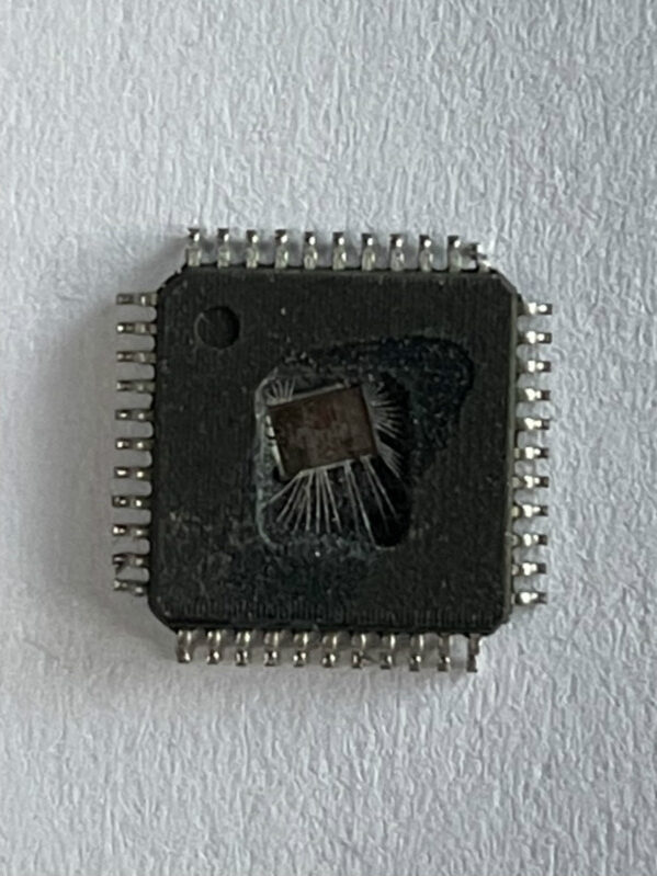
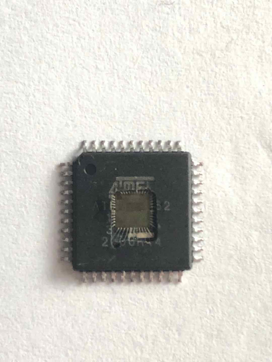
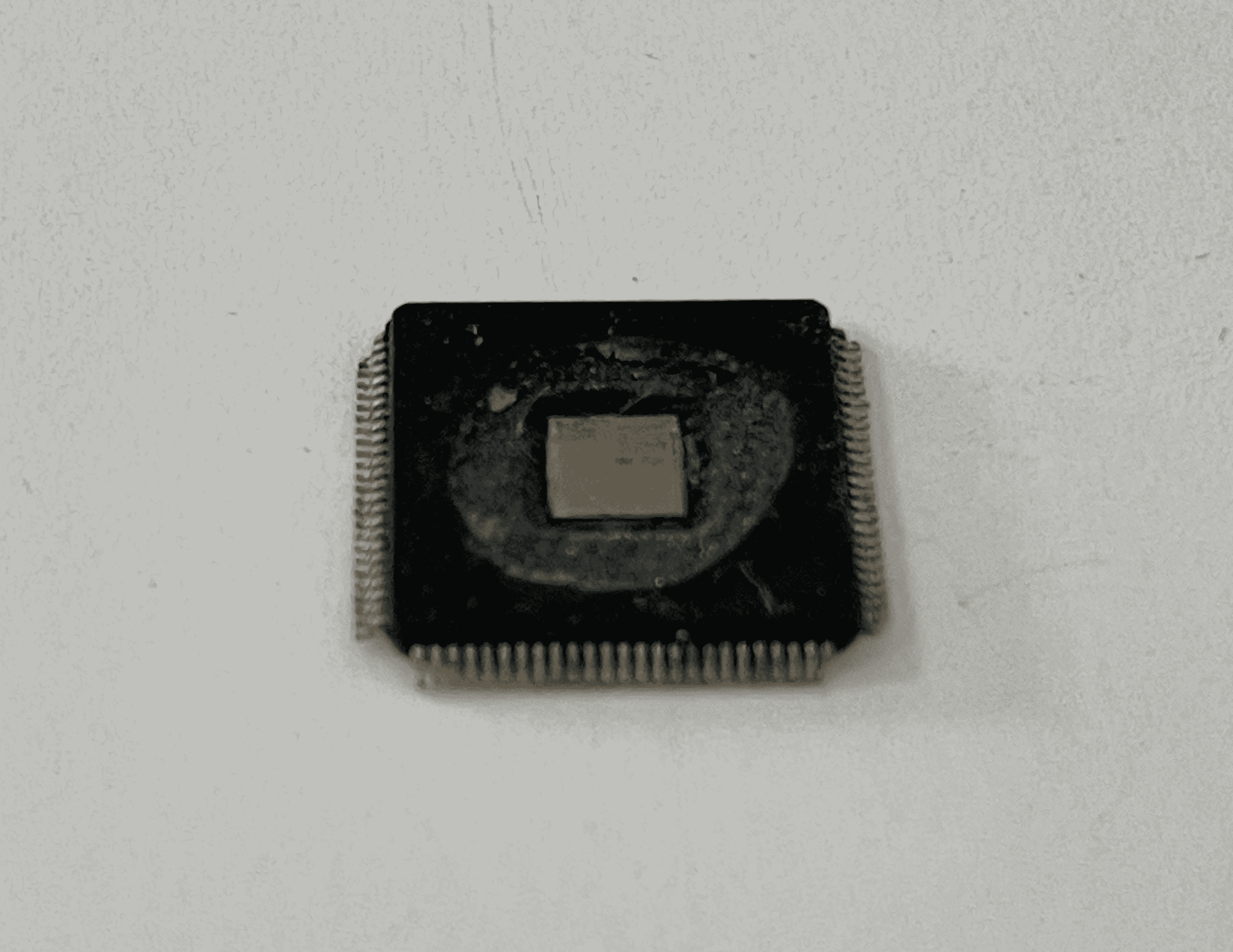
Break ARM STM32F072C8 Microcontroller Protection
Break ARM STM32F072C8 Microcontroller Protection over the flash memory, normally the fuse bit of MCU STM32F072C8 will be disable by processor cracking, and copy embedded heximal from flash memory of mcu stm32f072c8 to new MCU for cloning purpose;
System clock selection is performed on startup, however the internal RC 8 MHz oscillator is selected as default CPU clock on reset. An external 4-32 MHz clock can be selected, in which case it is monitored for failure. If failure is detected, the system automatically switches
back to the internal RC oscillator. A software interrupt is generated if enabled. Similarly, full interrupt management of the PLL clock entry is available when necessary (for example on failure of an indirectly used external crystal, resonator or oscillator).
Several prescalers allow the application to configure the frequency of the AHB and the APB domains. The maximum frequency of the AHB and the APB domains is 48 MHz.
Additionally, also the internal RC 48 MHz oscillator can be selected for system clock or PLL input source. This oscillator can be automatically fine-trimmed by the means of the CRS peripheral using the external synchronization.
ARM STM32F072CB Microcomputer Firmware Restoration
ARM STM32F072CB Microcomputer Firmware Restoration can help engineer to extract embedded source code from stm32f072cb mcu chip flash memory, after unlock tamper resistance system of stm32f072cb microprocessor;
The CRC (cyclic redundancy check) calculation unit is used to get a CRC code using a configurable generator polynomial value and size. Among other applications, CRC-based techniques are used to verify data transmission or storage integrity.
In the scope of the EN/IEC 60335-1 standard, they offer a means of verifying the Flash memory integrity. The CRC calculation unit helps compute a signature of the software during runtime when decrypt the source code of stm32f071v8 mcu chip, to be compared with a reference signature generated at link- time and stored at a given memory location.
VDD = VDDIO1 = 2.0 to 3.6 V: external power supply for I/Os (VDDIO1) and the internal regulator. It is provided externally through VDD pins.
Il ripristino del firmware del microcomputer ARM STM32F072CB può aiutare l’ingegnere a estrarre il codice sorgente incorporato dalla memoria flash del chip MCU STM32F072CB, dopo aver sbloccato il sistema di resistenza alla manomissione del microprocessore STM32F072CB;
VDDA = from VDD to 3.6 V: external analog power supply for ADC, DAC, Reset blocks, RCs and PLL (minimum voltage to be applied to VDDA is 2.4 V when the ADC or DAC are used). It is provided externally through VDDA pin. The VDDA voltage level must be always greater or equal to the VDD voltage level and must be established first.
VDDIO2 = 1.65 to 3.6 V: external power supply for marked I/Os. VDDIO2 is provided externally through the VDDIO2 pin. The VDDIO2 voltage level is completely independent from VDD or VDDA, but it must not be provided without a valid supply on VDD. The VDDIO2 supply is monitored and compared with the internal reference voltage (VREFINT) after reverse engineering stm32f071r8 arm microcomputer flash program. When the VDDIO2 is below this threshold, all the I/Os supplied from this rail are disabled by hardware. The output of this comparator is connected to EXTI line 31 and it can be used to generate an interrupt. Refer to the pinout diagrams or tables for concerned I/Os list.
VBAT = 1.65 to 3.6 V: power supply for RTC, external clock 32 kHz oscillator and backup registers (through power switch) when VDD is not present.
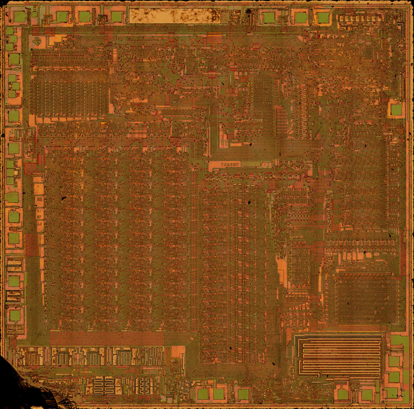
Reverse Engineering ARM Microcontroller STM32F072R8 Flash Memory
Reverse Engineering ARM Microcontroller STM32F072R8 Flash Memory and readout embedded heximal file from stm32f072rb flash memory after crack microprocessor stm32f072rb locked bit by focus ion beam technique;
The device has the following features:
16 Kbytes of embedded SRAM accessed (read/write) at CPU clock speed with 0 wait states and featuring embedded parity checking with exception generation for fail-critical applications.
The non-volatile memory is divided into two arrays:
64 to 128 Kbytes of embedded Flash memory for programs and data when hack stm32f071vb mcu flash memory protection
Option bytes
The option bytes are used to write-protect the memory (with 4 KB granularity) and/or readout-protect the whole memory with the following options:
Level 0: no readout protection
reverse engineering microcontrollore ARM STM32F072R8 memoria flash e lettura file eshimale incorporato da STM32F072RB memoria flash dopo crack microprocessore STM32F072RB bit bloccato dalla tecnica del fascio ionico di messa a fuoco
Level 1: memory readout protection, the Flash memory cannot be read from or written to if either debug features are connected or boot in RAM is selected by breaking stm32f071rb microcontroller locked bit;
Level 2: chip readout protection, debug features (Arm® Cortex®-M0 serial wire) and boot in RAM selection disabled
At startup, the boot pin and boot selector option bit are used to select one of the three boot options:
boot from User Flash memory
boot from System Memory
boot from embedded SRAM
The boot loader is located in System Memory. It is used to reprogram the Flash memory by using USART on pins PA14/PA15, or PA9/PA10 or I2C on pins PB6/PB7 or through the USB DFU interface.
ARM Microcomputer STM32F072R8 Readout Protection Breaking
ARM Microcomputer STM32F072R8 Readout Protection Breaking can unlock the fuse bit applied over microcontroller stm32f072r8 flash memory, and then readout embedded heximal from stm32f072r8 mcu;
The STM32F072x8/xB microcontrollers include devices in seven different packages ranging from 48 pins to 100 pins with a die form also available upon request. Depending on the device chosen, different sets of peripherals are included which will bring more difficult for recover stm32f051c4 microprocessor flash binary.
La rottura della protezione di lettura del microcomputer ARM STM32F072R8 può sbloccare la punta del fusibile applicata sulla memoria flash del microcontrollore stm32f072r8 e quindi leggere l’heximal incorporato dall’MCU stm32f072r8;
These features make the STM32F072x8/xB microcontrollers suitable for a wide range of applications such as application control and user interfaces, hand-held equipment, A/V receivers and digital TV, PC peripherals, gaming and GPS platforms, industrial applications, PLCs, inverters, printers, scanners, alarm systems, video intercoms and HVACs.
The Arm® Cortex®-M0 is a generation of Arm 32-bit RISC processors for embedded systems. It has been developed to provide a low-cost platform that meets the needs of MCU implementation, with a reduced pin count and low-power consumption, while delivering outstanding computational performance and an advanced system response to interrupts.
The Arm® Cortex®-M0 processors feature exceptional code-efficiency, delivering the high performance expected from an Arm core, with memory sizes usually associated with 8- and 16-bit devices. The STM32F072x8/xB devices embed Arm core and are compatible with all Arm tools and software which is suitable for breaking stm32f071rb microcontroller locked bits protection over flash memory content.
Arm Microprocessor STM32F072RB CPU Reverse Engineering
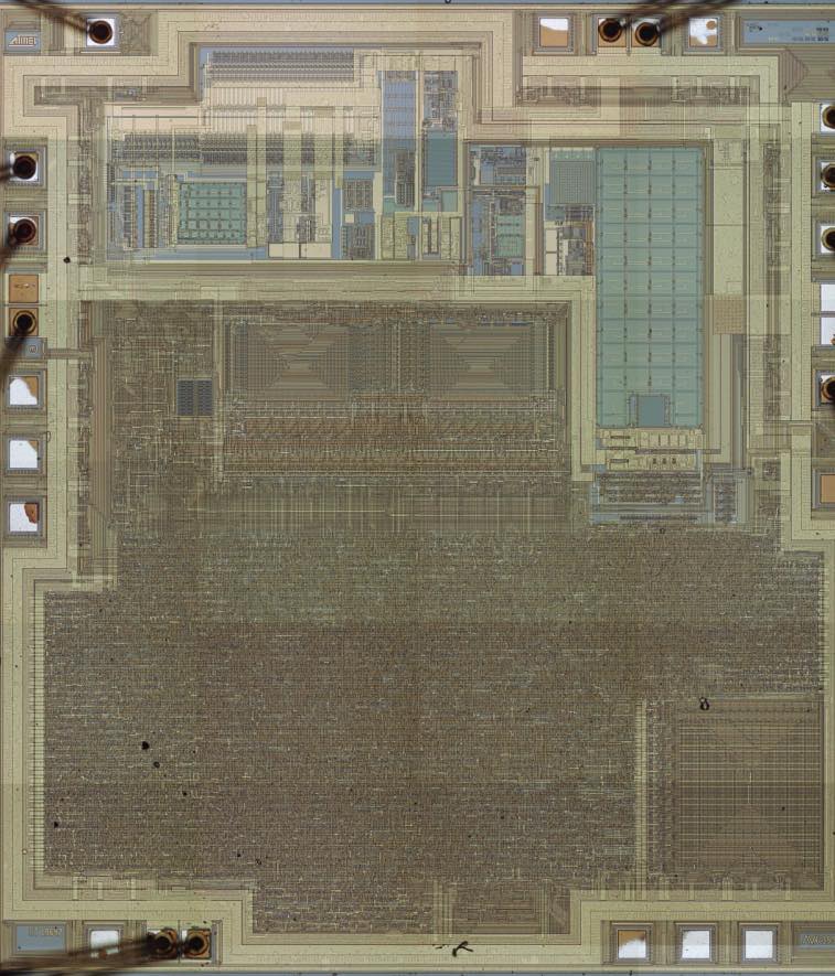
Arm Microprocessor STM32F072RB CPU Reverse Engineering starts from delayer the microcontroller structure one by one in the reverse order of MCU production, which is also called mcu stm32f072rb cracking, finally purpose of this execution is to have the embedded heximal file extracted from microprocessor stm32f072rb flash memory;
This datasheet provides characteristics and ordering information of the STM32F072x8/xB microcontrollers.
This document should be read in conjunction with the STM32F0xxxx reference manual (RM0091). The reference manual is available from the STMicroelectronics website www.st.com. For information on the Arm®(a)Cortex®-M0 core, please refer to the Arm® Cortex®-M0 Technical Reference Manual, available from the www.arm.com website.
The STM32F072x8/xB microcontrollers incorporate the high-performance Arm®Cortex®-M0 32-bit RISC core operating at up to 48 MHz frequency, high-speed embedded memories (up to 128 Kbytes of Flash memory and 16 Kbytes of SRAM), and an extensive range of enhanced peripherals and I/Os.
Il reverse engineering della CPU del microprocessore STM32F072RB inizia dal delayer della struttura del microcontrollore uno per uno nell’ordine inverso della produzione MCU, che è anche chiamato cracking MCU STM32F072RB, infine lo scopo di questa esecuzione è quello di avere il file exical incorporato estratto dalla memoria flash del microprocessore STM32F072RB;
All devices offer standard communication interfaces (two I2Cs, two SPI/I2S, one HDMI CEC and four USARTs), one USB Full-speed device (crystal-less), one CAN, one 12-bit ADC, one 12-bit DAC with two channels, seven 16-bit timers, one 32-bit timer and an advanced-control PWM timer.
The STM32F072x8/xB microcontrollers operate in the -40 to +85 °C and -40 to +105 °C temperature ranges, from a 2.0 to 3.6 V power supply. A comprehensive set of power-saving modes allows the design of low-power applications by decrypting source code of stm32f071v8 mcu flash memory.
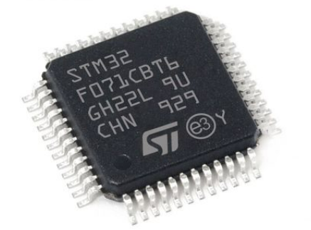
Reverse ARM Microcomputer STM32F071R8 Flash Program
Reverse ARM Microcomputer STM32F071R8 Flash Program is a process to crack arm mcu stm32f071r8 locked bit and disable the protection over its flash memory, after copying the extracted heximal to new processor stm32f071r8 for functions clones;

The current consumption of the on-chip peripherals is given in Table 35. The MCU is placed under the following conditions:
- All I/O pins are in analog mode
- All peripherals are disabled unless otherwise mentioned
- The given value is calculated by measuring the current consumption
- with all peripherals clocked off
- with only one peripheral clocked on
- Ambient operating temperature and supply voltage conditions summarized in Table 21: Voltage characteristics
The power consumption of the digital part of the on-chip peripherals is given in the process of arm microcontroller stm32f071vb source code decryption. The power consumption of the analog part of the peripherals (where applicable) is indicated in each related section of the datasheet.
In bypass mode the LSE oscillator is switched off and the input pin is a standard GPIO. The external clock signal has to respect the I/O characteristics in Section 6.3.14. However, the recommended clock input waveform is shown in Figure 15.
The high-speed external (HSE) clock can be supplied with a 4 to 32 MHz crystal/ceramic resonator oscillator. All the information given in this paragraph are based on design simulation results obtained with typical external components specified to hack stm32f071vb mcu flash memory binary.
Il reverse engineering della CPU del microprocessore STM32F072RB inizia dal delayer della struttura del microcontrollore uno per uno nell’ordine inverso della produzione MCU, che è anche chiamato cracking MCU STM32F072RB, infine lo scopo di questa esecuzione è quello di avere il file exical incorporato estratto dalla memoria flash del microprocessore STM32F072RB;
In the application, the resonator and the load capacitors have to be placed as close as possible to the oscillator pins in order to minimize output distortion and startup stabilization time. Refer to the crystal resonator manufacturer for more details on the resonator characteristics (frequency, package, accuracy).
ARM STM32F071RB Microcontroller Locked Bit Breaking
After ARM STM32F071RB Microcontroller Locked Bit Breaking has been completed, the stm32f071rb chip firmware can be decoded and then clone binary content to new microprocessor;

The current consumption of the I/O system has two components: static and dynamic.
I/O static current consumption
All the I/Os used as inputs with pull-up generate current consumption when the pin is externally held low. The value of this current consumption can be simply computed by using the pull-up/pull-down resistors values given in Table 53: I/O static characteristics.
For the output pins, any external pull-down or external load must also be considered to estimate the current consumption. Additional I/O current consumption is due to I/Os configured as inputs if an intermediate voltage level is externally applied to recover stm32f051c4 mcu flash binary file.
dopo che il bit breaking bloccato del microcontrollore ARM STM32F071RB è stato completato, il firmware del chip STM32F071RB può essere decodificato e quindi clonare il contenuto binario sul nuovo microprocessore;
This current consumption is caused by the input Schmitt trigger circuits used to discriminate the input value. Unless this specific configuration is required by the application, this supply current consumption can be avoided by configuring these I/Os in analog mode. This is notably the case of ADC input pins which should be configured as analog inputs.
Any floating input pin can also settle to an intermediate voltage level or switch inadvertently, as a result of external electromagnetic noise. To avoid current consumption related to floating pins, they must either be configured in analog mode for the sake of restore microprocessor stm32f051c6 flash heximal, or forced internally to a definite digital value. This can be done either by using pull-up/down resistors or by configuring the pins in output mode.
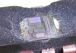
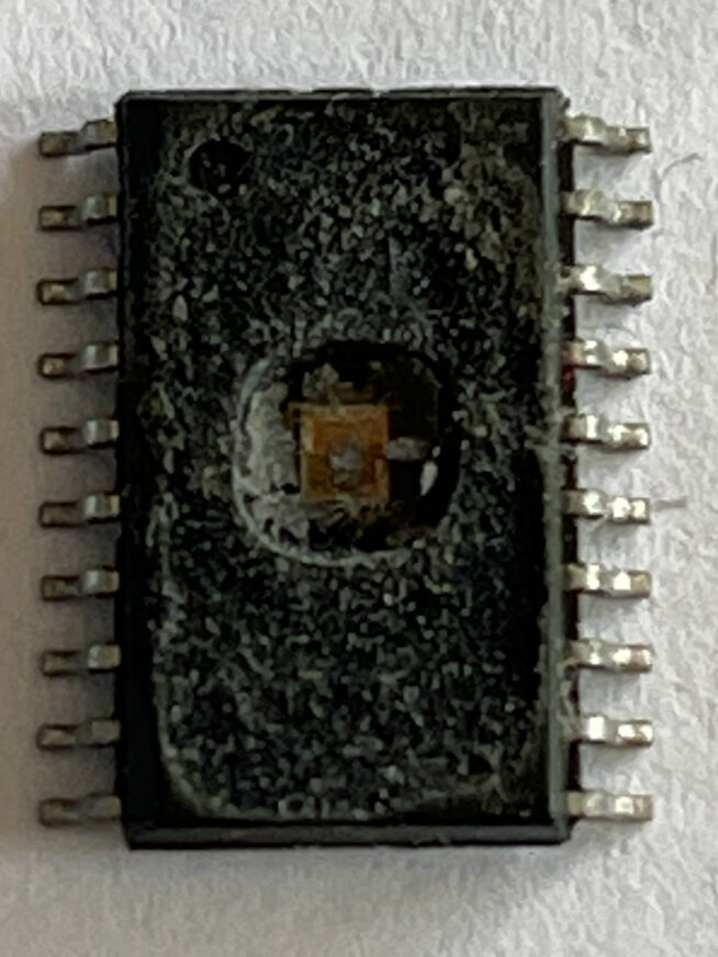
Hack ARM STM32F071VB MCU Flash Memory Protection
Hack ARM STM32F071VB MCU Flash Memory Protection needs to apply an invasive cracking method normally starts from decapsulate the silicon package over microcontroller stm32f071vb processor, and then readout the unlocked microprocessor stm32f071vb flash code directly;
Up to two I2C interfaces (I2C1 and I2C2) can operate in multimaster or slave modes. Both can support Standard mode (up to 100 kbit/s) or Fast mode (up to 400 kbit/s). I2C1 also supports Fast Mode Plus (up to 1 Mbit/s), with 20 mA output drive. Both support 7-bit and 10-bit addressing modes, multiple 7-bit slave addresses (two addresses, one with configurable mask). They also include programmable analog and digital noise filters.
In addition, I2C1 provides hardware support for SMBUS 2.0 and PMBUS 1.1: ARP capability, Host notify protocol, hardware CRC (PEC) generation/verification by recover flash data from locked stm32f071rb mcu, timeouts verifications and ALERT protocol management. The I2C interfaces can be served by the DMA controller.
hack ARM STM32F071VB La protezione della memoria flash MCU deve applicare un metodo di cracking invasivo che normalmente inizia dal decapsulare il pacchetto di silicio sul processore STM32F071VB del microcontrollore e quindi leggere direttamente il codice flash del microprocessore sbloccato STM32F071VB;
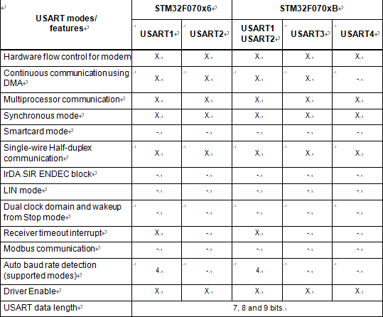
The device embeds up to four universal synchronous/asynchronous receivers/transmitters that communicate at speeds of up to 6 Mbit/s. belwo Table gives an overview of features as implemented on the available USART interfaces. All USART interfaces can be served by the DMA controller.