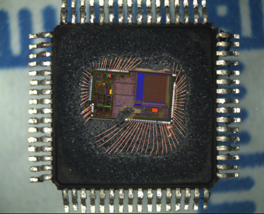
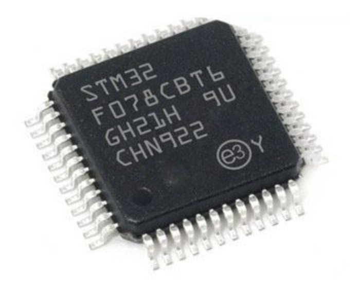
 Break STM32F038C6 MCU Locked Flash Memory
Break STM32F038C6 MCU Locked Flash Memory protection and readout embedded heximal file from microprocessor stm32f038c6 memory, the fuse bit of stm32f038c6 will be unlocked in order to extract source code;
The STM32F038x6 microcontrollers incorporate the high-performance ARM® Cortex®-M0 32-bit RISC core operating at up to 48 MHz frequency, high-speed embedded memories (32 Kbytes of Flash memory and 4 Kbytes of SRAM), and an extensive range of enhanced peripherals and I/Os.
All devices offer standard communication interfaces (one I2C, one SPI/ I2S and one USART), one 12-bit ADC, five 16-bit timers, one 32-bit timer and an advanced-control PWM timer when recover flash firmware from stm32f031e6 microcontroller.

сломать защиту заблокированной флэш-памяти STM32F038C6 MCU и считывание встроенного шестнадцатеричного файла из памяти микропроцессора STM32F038C6, бит предохранителя STM32F038C6 будет разблокирован для извлечения исходного кода;
The STM32F038x6 microcontrollers operate in the -40 to +85 °C and -40 to +105 °C temperature ranges at a 1.8 V ± 8% power supply. A comprehensive set of power-saving modes allows the design of low-power applications.
The STM32F038x6 microcontrollers include devices in five different packages ranging from 20 pins to 48 pins with a die form also available upon request. Depending on the device chosen, different sets of peripherals are included.
These features make the STM32F038x6 microcontrollers suitable for a wide range of applications such as application control and user interfaces, hand-held equipment in order to reverse engineering mcu stm32f031f4 microprocessor source code, A/V receivers and digital TV, PC peripherals, gaming and GPS platforms, industrial applications, PLCs, inverters, printers, scanners, alarm systems, video intercoms and HVACs.
Reverse ARM STM32F031F4 Microprocessor Source Code
Reverse ARM STM32F031F4 Microprocessor Source Code from its flash memory, and copy flash firmware to new mcu stm32f031f4 by programmer, the locked bits of microcontroller stm32f031f4 has been disabled by mcu cracking technique;
The MCU is placed under the following conditions:
- VDD = VDDA = 3.3 V
- All I/O pins are in analog input configuration
- The Flash memory access time is adjusted to fHCLK frequency:
- 0 wait state and Prefetch OFF from 0 to 24 MHz
- 1 wait state and Prefetch ON above 24 MHz
- When the peripherals are enabled, fPCLK = fHCLK
- PLL is used for frequencies greater than 8 MHz
AHB prescaler of 2, 4, 8 and 16 is used for the frequencies 4 MHz, 2 MHz, 1 MHz and 500 kHz respectively.
The current consumption of the I/O system has two components: static and dynamic when recover flash firmware from stm32f031e6 arm microcontroller.
All the I/Os used as inputs with pull-up generate current consumption when the pin is externally held low. The value of this current consumption can be simply computed by using the pull-up/pull-down resistors values given in Table 46: I/O static characteristics.
обратный исходный код микропроцессора ARM STM32F031F4 из его флэш-памяти и копирование прошивки флэш-памяти на новый микроконтроллер STM32F031F4 с помощью программиста, заблокированные биты микроконтроллера STM32F031F4 были отключены методом взлома микроконтроллера;
For the output pins, any external pull-down or external load must also be considered to estimate the current consumption. Additional I/O current consumption is due to I/Os configured as inputs if an intermediate voltage level is externally applied by breaking arm microprocessor stm32f030cc flash memory.
This current consumption is caused by the input Schmitt trigger circuits used to discriminate the input value. Unless this specific configuration is required by the application, this supply current consumption can be avoided by configuring these I/Os in analog mode. This is notably the case of ADC input pins which should be configured as analog inputs.
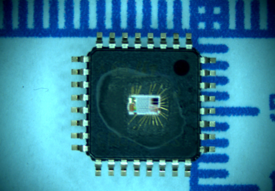
ARM Microcontroller STM32F031E6 Flash Firmware Recovery
ARM Microcontroller STM32F031E6 Flash Firmware Recovery starts from unlock fuse bit which has been used to secure microprocessor stm32f031e6 mcu, and then extract embedded heximal file from mcu stm32f031e6;
The current consumption is a function of several parameters and factors such as the operating voltage, ambient temperature, I/O pin loading, device software configuration, operating frequencies, I/O pin switching rate, program location in memory and executed binary code.
All Run-mode current consumption measurements given in this section are performed with a reduced code that gives a consumption equivalent to CoreMark code when breaking arm microprocessor stm32f030r8 locked bits.
एआरएम माइक्रोकंट्रोलर एसटीएम 32एफ031ई6 फ्लैश फर्मवेयर रिकवरी अनलॉक फ्यूज बिट से शुरू होती है जिसका उपयोग माइक्रोप्रोसेसर एसटीएम 32एफ031ई6 एमसीयू को सुरक्षित करने के लिए किया गया है, और फिर एमसीयू एसटीएम 32 एफ 031 ई 6 से एम्बेडेड हेक्सिमल फ़ाइल निकालता है;
The MCU is placed under the following conditions:
- All I/O pins are in analog input mode
- All peripherals are disabled except when explicitly mentioned
- The Flash memory access time is adjusted to the fHCLK frequency:
- 0 wait state and Prefetch OFF from 0 to 24 MHz
- 1 wait state and Prefetch ON above 24 MHz
When the peripherals are enabled fPCLK = fHCLK
- Current consumption from the VDDA supply is independent of whether the digital peripherals are enabled or disabled, being in Run or Sleep mode or executing from Flash memory or RAM by attacking stm32f030c8 microcontroller readout protection. Furthermore, when the PLL is off, IDDA is independent of clock frequencies.
- Data based on characterization results, not tested in production unless otherwise specified.
Data based on characterization results and tested in production (using one common test limit for sum of IDD and IDDA).
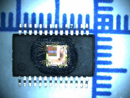
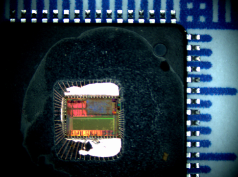
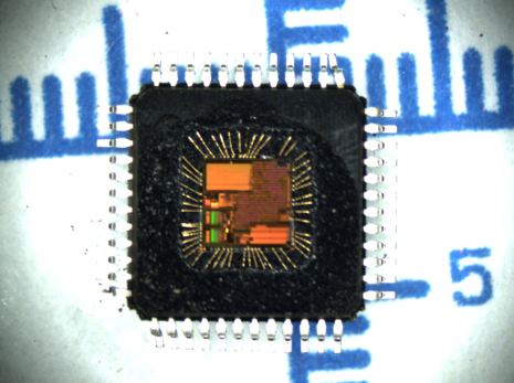
Break ARM Microprocessor STM32F030CC Flash Memory
Break ARM Microprocessor STM32F030CC Flash Memory and clone embedded heximal from mcu stm32f030cc flash memory, the readout protection will be disable and source code of microcontroller stm32f030cc will be extracted;
The internal voltage reference (VREFINT) provides a stable (bandgap) voltage output for the ADC. VREFINT is internally connected to the ADC_IN17 input channel. The precise voltage of VREFINT is individually measured for each part by ST during production test and stored in the system memory area. It is accessible in read-only mode.
The advanced-control timer (TIM1) can be seen as a three-phase PWM multiplexed on six channels to attack secured cpu stm32f070rb locked bit. It has complementary PWM outputs with programmable inserted dead times. It can also be seen as a complete general-purpose timer. The four independent channels can be used for:
एआरएम माइक्रोप्रोसेसर एसटीएम 32 एफ 030 सीसी फ्लैश मेमोरी और एमसीयू एसटीएम 32 एफ 030 सीसी फ्लैश मेमोरी से क्लोन एम्बेडेड हेक्सिमल को तोड़ें, रीडआउट सुरक्षा अक्षम हो जाएगी और माइक्रोकंट्रोलर एसटीएम 32 एफ 030 सीसी का स्रोत कोड निकाला जाएगा;
- Input capture
- Output compare
- PWM generation (edge or center-aligned modes)
- One-pulse mode output
If configured as a standard 16-bit timer, it has the same features as the TIMx timer. If configured as the 16-bit PWM generator, it has full modulation capability (0-100%).
The counter can be frozen in debug mode. Many features are shared with those of the standard timers which have the same architecture. The advanced control timer can therefore work together with the other timers via the Timer Link feature for synchronization or event chaining by breaking stm32f030r8 microprocessor locked bits.
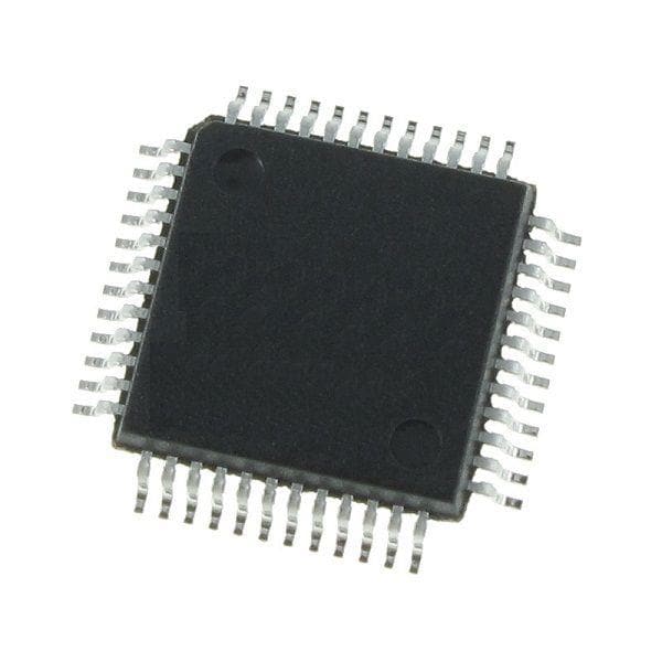
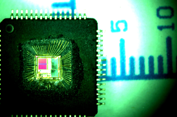
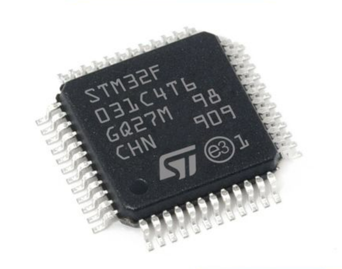
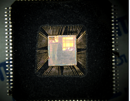
ARM MCU STM32F031C4 Flash Memory Breaking
ARM MCU STM32F031C4 Flash Memory Breaking is a process to crack microprocessor stm32f031c4 flash memory security fuse bit, and then extract flash binary from stm32f031c4 arm microcontroller;
The STM32F031x4/x6 microcontrollers incorporate the high-performance ARM® Cortex®- M0 32-bit RISC core operating at up to 48 MHz frequency, high-speed embedded memories (up to 32 Kbytes of Flash memory and 4 Kbytes of SRAM) to break stm32f030r8 mcu locked bits, and an extensive range of enhanced peripherals and I/Os. All devices offer standard communication interfaces (one I2C, one SPI/ I2S and one USART), one 12-bit ADC, five 16-bit timers, one 32-bit timer and an advanced-control PWM timer.
The STM32F031x4/x6 microcontrollers operate in the -40 to +85 °C and -40 to +105 °C temperature ranges, from a 2.0 to 3.6 V power supply. A comprehensive set of power-saving modes allows the design of low-power applications.
एआरएम एमसीयू एसटीएम 32 एफ 031 सी 4 फ्लैश मेमोरी ब्रेकिंग माइक्रोप्रोसेसर एसटीएम 32 एफ 031 सी 4 फ्लैश मेमोरी सिक्योरिटी फ्यूज बिट को क्रैक करने की एक प्रक्रिया है, और फिर एसटीएम 32 एफ 031 सी 4 आर्म माइक्रोकंट्रोलर से फ्लैश बाइनरी निकालने के लिए;
The STM32F031x4/x6 microcontrollers include devices in six different packages ranging from 20 pins to 48 pins with a die form also available upon request. Depending on the device chosen, different sets of peripherals are included when attacking stm32f070rb arm mcu locked bits.
These features make the STM32F031x4/x6 microcontrollers suitable for a wide range of applications such as application control and user interfaces, hand-held equipment, A/V receivers and digital TV, PC peripherals, gaming and GPS platforms, industrial applications, PLCs, inverters, printers, scanners, alarm systems, video intercoms and HVACs.
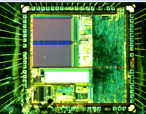
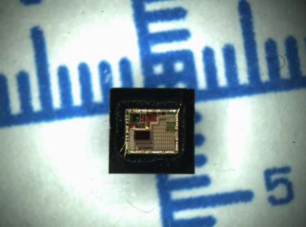
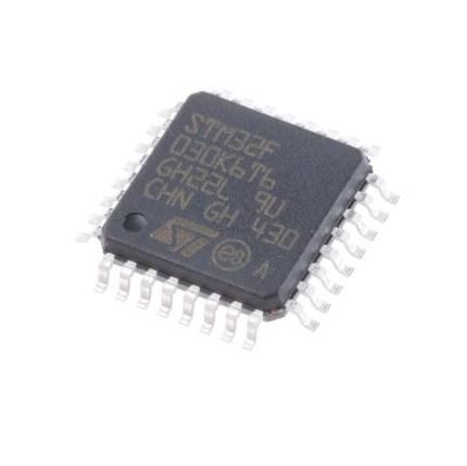
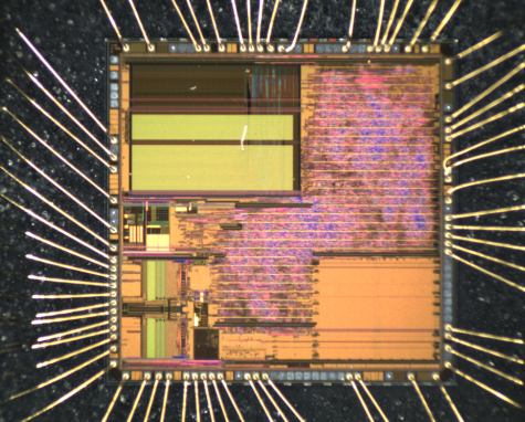
STM32F030K6 Microprocessor Secured Heximal Restoration
STM32F030K6 Microprocessor Secured Heximal Restoration needs to clone stm32f030k6 mcu locked bit by focus ion beam and then copy embedded firmware to new microcontroller stm32f030k6 flash memory;
The 12-bit analog to digital converter has up to 16 external and two internal (temperature sensor, voltage reference measurement) channels and performs conversions in single-shot or scan modes. In scan mode, automatic conversion is performed on a selected group of analog inputs.
The ADC can be served by the DMA controller. An analog watchdog feature allows very precise monitoring of the converted voltage of one, some or all selected channels by cracking stm32f071vc flash memory protection. An interrupt is generated when the converted voltage is outside the programmed thresholds.
La restauración hexamal asegurada por microprocesador STM32F030K6 necesita clonar el MCU STM32F030K6 bloqueado bit por haz de iones de enfoque y luego copiar el firmware integrado a la nueva memoria flash del microcontrolador STM32F030K6;
The temperature sensor (TS) generates a voltage VSENSE that varies linearly with temperature. The temperature sensor is internally connected to the ADC_IN16 input channel which is used to convert the sensor output voltage into a digital value.
The sensor provides good linearity but it has to be calibrated to obtain good overall accuracy of the temperature measurement. As the offset of the temperature sensor varies from chip to chip due to process variation, the uncalibrated internal temperature sensor is suitable for applications that detect temperature changes only by attacking stm32f070rb microcontroller flash memory.
To improve the accuracy of the temperature sensor measurement, each device is individually factory-calibrated by ST. The temperature sensor factory calibration data are stored by ST in the system memory area, accessible in read-only mode.
Break ARM STM32F030R8 Microprocessor Locked Bits
Break ARM STM32F030R8 Microprocessor Locked Bits to disable its tamper resistance system, and readout flash memory software from mcu stm32f030r8, then duplicate firmware to new microcontroller stm32f030r8;
System clock selection is performed on startup, however the internal RC 8 MHz oscillator is selected as default CPU clock on reset. An external 4-32 MHz clock can be selected, in which case it is monitored for failure.
If failure is detected, the system automatically switches back to the internal RC oscillator. A software interrupt is generated if enabled. Similarly, full interrupt management of the PLL clock entry is available when necessary (for example on failure of an indirectly used external crystal, resonator or oscillator) by cracking stm32f070cb mcu flash memory.
romper los bits bloqueados del microprocesador ARM STM32F030R8 para desactivar su sistema de resistencia a la manipulación y leer el software de memoria flash del MCU STM32F030R8, luego duplicar el firmware al nuevo microcontrolador STM32F030R8;
Several prescalers allow the application to configure the frequency of the AHB and the APB domains. The maximum frequency of the AHB and the APB domains is 48 MHz.
Each of the GPIO pins can be configured by software as output (push-pull or open-drain), as input (with or without pull-up or pull-down) or as peripheral alternate function. Most of the GPIO pins are shared with digital or analog alternate functions by restore stm32f071cb microcontroller flash memory binary file. The I/O configuration can be locked if needed following a specific sequence in order to avoid spurious writing to the I/Os registers.
Attack ARM STM32F030C8 Microcontroller Readout Protection
Attack ARM STM32F030C8 Microcontroller Readout Protection to be able to clone the embedded firmware from mcu stm32f030c8 flash memory, and then copy heximal to new microprocessor stm32f030c8 for functions replication;

The STM32F030x4/x6/x8/xC microcontrollers support three low-power modes to achieve the best compromise between low power consumption, short startup time and available wakeup sources:
· Sleep mode
In Sleep mode, only the CPU is stopped. All peripherals continue to operate and can wake up the CPU when an interrupt/event occurs.
· Stop mode
Stop mode achieves very low power consumption while retaining the content of SRAM and registers. All clocks in the 1.8 V domain are stopped, the PLL in the process of cracking stm32f071vc mcu protection system, the HSI RC and the HSE crystal oscillators are disabled. The voltage regulator can also be put either in normal or in low power mode.
ataque Protección de lectura del microcontrolador ARM STM32F030C8 para poder clonar el firmware integrado de la memoria flash MCU STM32F030C8 y luego copiar hexamal al nuevo microprocesador STM32F030C8 para la replicación de funciones;
The device can be woken up from Stop mode by any of the EXTI lines. The EXTI line source can be one of the 16 external lines and RTC.
· Standby mode
The Standby mode is used to achieve the lowest power consumption. The internal voltage regulator is switched off so that the entire 1.8 V domain is powered off. The PLL, the HSI RC and the HSE crystal oscillators are also switched off. After entering Standby mode for the sake of attacking stm32f070rb arm mcu locked bit, SRAM and register contents are lost except for registers in the RTC domain and Standby circuitry. The device exits Standby mode when an external reset (NRST pin), an IWDG reset, a rising edge on the WKUP pins, or an RTC event occurs.
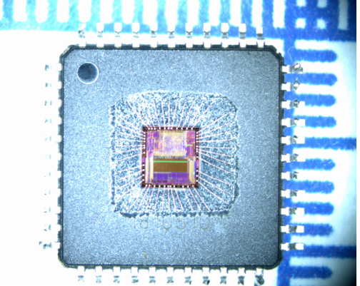
Reverse Engineering ARM STM32F078R8 MCU
Reverse Engineering ARM STM32F078R8 MCU process will help engineer to figure out how to crack stm32f078r8 microcontroller fuse bit by focus ion beam and then readout embedded heximal file from stm32f078r8 microprocessor’s flash memory;
The internal voltage reference (VREFINT) provides a stable (bandgap) voltage output for the ADC and comparators. VREFINT is internally connected to the ADC_IN17 input channel. The precise voltage of VREFINT is individually measured for each part by ST during production test and stored in the system memory area. It is accessible in read-only mode.
This embedded hardware feature allows the application to measure the VBAT battery voltage using the internal ADC channel ADC_IN18. As the VBAT voltage may be higher than VDDA after breaking stm32f071rb microcontroller locked bit, and thus outside the ADC input range, the VBAT pin is internally connected to a bridge divider by 2. As a consequence, the converted digital value is half the VBAT voltage.
El proceso de ingeniería inversa de MCU ARM STM32F078R8 ayudará al ingeniero a descubrir cómo descifrar el fusible del microcontrolador STM32F078R8 bit a haz de iones de enfoque y luego leer el archivo hexamal incrustado de la memoria flash del microprocesador STM32F078R8;
The two 12-bit buffered DAC channels can be used to convert digital signals into analog voltage signal outputs. The chosen design structure is composed of integrated resistor strings and an amplifier in non-inverting configuration.
This digital Interface supports the following features:
- 8-bit or 12-bit monotonic output
- Left or right data alignment in 12-bit mode
- Synchronized update capability
- Noise-wave generation
- Triangular-wave generation
- Dual DAC channel independent or simultaneous conversions
- DMA capability for each channel
- External triggers for conversion
Six DAC trigger inputs are used in the device. The DAC is triggered through the timer trigger outputs and the DAC interface is generating its own DMA requests to reverse stm32f071r8 arm microcomputer flash program.
Reverse Engineer STM32F078VB Microcontroller Program
Reverse Engineer STM32F078VB Microcontroller Program actually is a process to clone a microprocessor stm32f078vb with the same heximal from its flash memory, original embedded firmware will be extracted from mcu stm32f078v8;
The Arm® Cortex®-M0 is a generation of Arm 32-bit RISC processors for embedded systems. It has been developed to provide a low-cost platform that meets the needs of MCU implementation, with a reduced pin count and low-power consumption, while delivering outstanding computational performance and an advanced system response to interrupts.
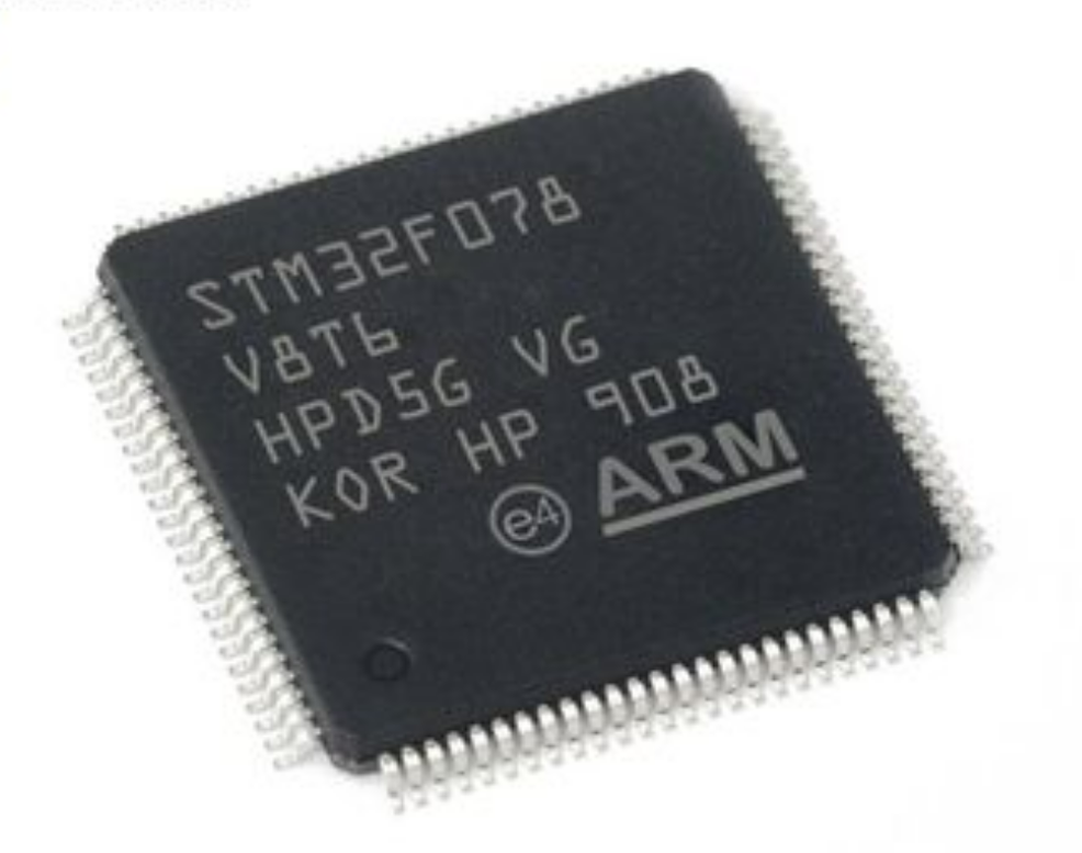
El programa de microcontrolador STM32F078VB de ingeniería inversa en realidad es un proceso para clonar un microprocesador STM32F078VB con el mismo hexamal de su memoria flash, el firmware integrado original se extraerá de MCU STM32F078V8;
The Arm® Cortex®-M0 processors feature exceptional code-efficiency, delivering the high performance expected from an Arm core, with memory sizes usually associated with 8- and 16-bit devices for stm32f071rb arm microcontroller memory locked bit breaking. The STM32F078CB/RB/VB devices embed Arm core and are compatible with all Arm tools and software.
The device has the following features:
- 16 Kbytes of embedded SRAM accessed (read/write) at CPU clock speed with 0 wait states and featuring embedded parity checking with exception generation for fail-critical applications.
- The non-volatile memory is divided into two arrays:
- 128 Kbytes of embedded Flash memory for programs and data
- Option bytes
- The non-volatile memory is divided into two arrays:
The option bytes are used to write-protect the memory (with 4 KB granularity) and/or readout-protect the whole memory with the following options:
- Level 0: no readout protection
- Level 1: memory readout protection, the Flash memory cannot be read from or written to if either debug features are connected or boot in RAM is selected which the stm32f071vb mcu flash memory can be hacked;
Level 2: chip readout protection, debug features (Arm® Cortex®-M0 serial wire) and boot in RAM selection disabled