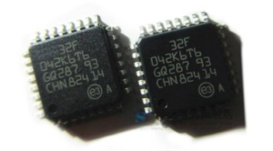
 Protective Microcontroller STM32F048C6 Flash Heximal Cracking
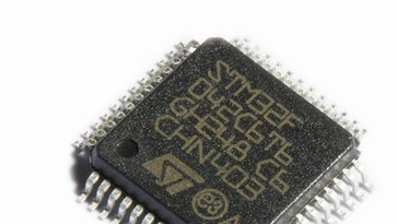
Protective Microcontroller STM32F048C6 Flash Heximal Cracking is a process to unlock the fuse bit used to secure embedded firmware of mcu stm32f048c6 and then dump heximal file to new microprocessor stm32f048c6.
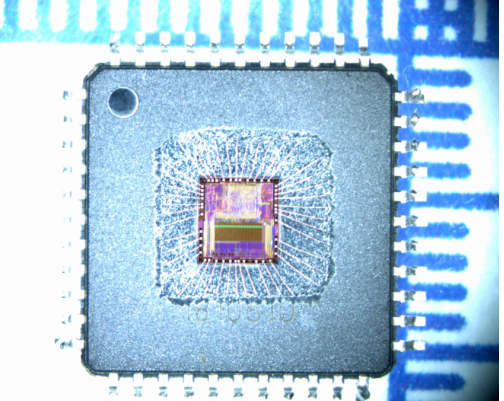
The STM32F048x6 microcontrollers incorporate the high-performance ARM® Cortex®-M0 32-bit RISC core operating at up to 48 MHz frequency, high-speed embedded memories (32 Kbytes of Flash memory and 6 Kbytes of SRAM), and an extensive range of enhanced peripherals and I/Os.
All devices offer standard communication interfaces (one I2C, two SPIs/one I2S, one HDMI CEC and two USARTs), one USB Full-speed device (crystal-less), one 12-bit ADC, four 16-bit timers, one 32-bit timer and an advanced-control PWM timer when breaking stm32f042g4 microcontroller flash heximal.
The STM32F048x6 microcontrollers operate in the -40 to +85 °C and -40 to +105 °C temperature ranges, at a 1.8 V ± 8% power supply. A comprehensive set of power-saving modes allows the design of low-power applications.
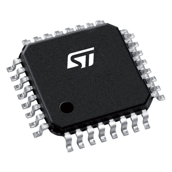
The STM32F048x6 microcontrollers include devices in three different packages ranging from 36 pins to 48 pins with a die form also available upon request. Depending on the device chosen, different sets of peripherals are included.
These features make the STM32F048x6 microcontrollers suitable for a wide range of applications such as application control and user interfaces, hand-held equipment in the process of recovering stm32f042k4 locked microprocessor firmware, A/V receivers and digital TV, PC peripherals, gaming and GPS platforms, industrial applications, PLCs, inverters, printers, scanners, alarm systems, video intercoms and HVACs.
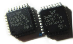
 Microcontroller STM32F042K6 Flash Locked Bit Breaking
Microcontroller STM32F042K6 Flash Locked Bit Breaking means the tamper resistance system of stm32f042k6 mcu will be cracked as well as readout protection, and then copying the heximal data to new microprocessor stm32f042k6 as mcu cloning;
The regulator has two operating modes and it is always enabled after reset.
- Main (MR) is used in normal operating mode (Run).
- Low power (LPR) can be used in Stop mode where the power demand is reduced.
In Standby mode, it is put in power down mode. In this mode, the regulator output is in high impedance and the kernel circuitry is powered down, inducing zero consumption (but the contents of the registers and SRAM are lost).
System clock selection is performed on startup, however the internal RC 8 MHz oscillator is selected as default CPU clock on reset by recover stm32f042f4 microcontroller embedded heximal program. An external 4-32 MHz clock can be selected, in which case it is monitored for failure. If failure is detected, the system automatically switches back to the internal RC oscillator.
la rotura de bits bloqueados por flash del microcontrolador STM32F042K6 significa que el sistema de resistencia a la manipulación del MCU STM32F042K6 se romperá, así como la protección de lectura, y luego copiará los datos hexamales al nuevo microprocesador STM32F042K6 como clonación de MCU;
A software interrupt is generated if enabled. Similarly, full interrupt management of the PLL clock entry is available when necessary (for example on failure of an indirectly used external crystal, resonator or oscillator).
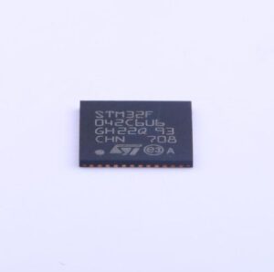
 Secured Microprocessor STM32F042C6 Flash Code Extraction
Secured Microprocessor STM32F042C6 Flash Code Extraction will needs to crack stm32f042c6 mcu security fuse bit by focus ion beam, and then dump embedded heximal file from stm32f042c6 flash memory;
The device has integrated power-on reset (POR) and power-down reset (PDR) circuits. They are always active, and ensure proper operation above a threshold of 2 V.
The device remains in reset mode when the monitored supply voltage is below a specified threshold, VPOR/PDR, without the need for an external reset circuit.
- The POR monitors only the VDD supply voltage. During the startup phase it is required that VDDA should arrive first and be greater than or equal to VDD.
- The PDR monitors both the VDD and VDDA supply voltages, however the VDDA power supply supervisor can be disabled (by programming a dedicated Option bit) to reduce the power consumption if the application design ensures that VDDA is higher than or equal to VDD.
The device features an embedded programmable voltage detector (PVD) that monitors the VDD power supply and compares it to the VPVD threshold when recovery stm32f042k4 microprocessor firmware. An interrupt can be generated when VDD drops below the VPVD threshold and/or when VDD is higher than the VPVD threshold.
защищенный микропроцессор STM32F042C6 для извлечения флэш-кода должен будет взломать предохранитель безопасности микроконтроллера STM32F042C6 с помощью фокусирующего ионного луча, а затем выгрузить встроенный шестигранный файл из флэш-памяти STM32F042C6;
The interrupt service routine can then generate a warning message and/or put the MCU into a safe state. The PVD is enabled by software.
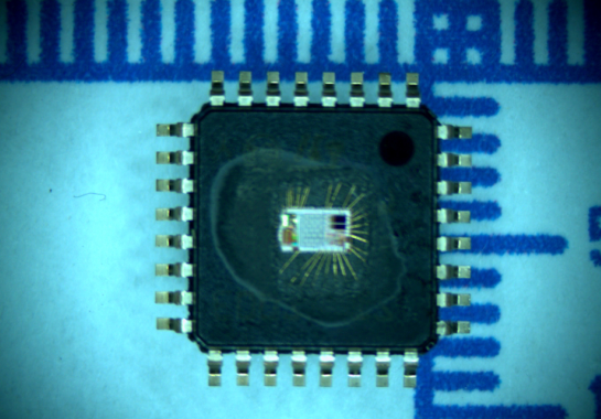
 Recover STM32F042K4 Locked Microprocessor Firmware
Recover STM32F042K4 Locked Microprocessor Firmware from its flash memory, after breaking stm32f042k4 microcontroller readout protection, and flash data can be replicated from stm32f042k4 mcu chip;
The device has the following features:
- 6 Kbytes of embedded SRAM accessed (read/write) at CPU clock speed with 0 wait states and featuring embedded parity checking with exception generation for fail-critical applications.
- The non-volatile memory is divided into two arrays:
- 16 to 32 Kbytes of embedded Flash memory for programs and data
- Option bytes
- The non-volatile memory is divided into two arrays:
The option bytes are used to write-protect the memory (with 4 KB granularity) and/or readout-protect the whole memory with the following options:
- Level 0: no readout protection
- Level 1: memory readout protection, the Flash memory cannot be read from or written to if either debug features are connected or boot in RAM is selected
- Level 2: chip readout protection, debug features (Cortex®-M0 serial wire) and boot in RAM selection disabled
At startup, the boot pin and boot selector option bits are used to select one of the three boot options:
- boot from User Flash memory
- boot from System Memory
- boot from embedded SRAM
The boot pin is shared with the standard GPIO and can be disabled through the boot selector option bits. The boot loader is located in System Memory. It is used to reprogram the Flash memory by using USART on pins PA14/PA15, or PA9/PA10 or I2C on pins PB6/PB7 or through the USB DFU interface.
 Microcontroller STM32F042G4 Flash Memory Breaking
Microcontroller STM32F042G4 Flash Memory Breaking will help engineer to be able to replicate microprocessor stm32f042g4 flash program, normally it is required to decode stm32f042g4 microcontroller embedded firmware into the re-programming mode;
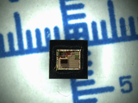
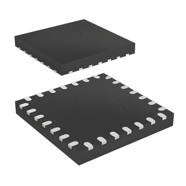
The STM32F042x4/x6 microcontrollers include devices in seven different packages ranging from 20 pins to 48 pins with a die form also available upon request. Depending on the device chosen, different sets of peripherals are included.
These features make the STM32F042x4/x6 microcontrollers suitable for a wide range of applications such as application control and user interfaces, hand-held equipment, A/V receivers and digital TV, PC peripherals, gaming and GPS platforms, industrial applications, PLCs, inverters, printers, scanners, alarm systems, video intercoms and HVACs.
взлом флэш-памяти микроконтроллера STM32F042G4 поможет инженеру реплицировать программу флэш-памяти микропроцессора STM32F042G4, обычно требуется декодировать встроенное микропрограммное обеспечение микроконтроллера STM32F042G4 в режим перепрограммирования;
The ARM® Cortex®-M0 is a generation of ARM 32-bit RISC processors for embedded systems. It has been developed to provide a low-cost platform that meets the needs of MCU implementation, with a reduced pin count and low-power consumption in the process of breaking stm32f038c6 locked mcu flash memory, while delivering outstanding computational performance and an advanced system response to interrupts.
The ARM® Cortex®-M0 processors feature exceptional code-efficiency, delivering the high performance expected from an ARM core, with memory sizes usually associated with 8- and 16-bit devices. The STM32F042x4/x6 devices embed ARM core and are compatible with all ARM tools and software.
 Protected STM32F042F4 Microcontroller Program Recovery
Protected STM32F042F4 Microcontroller Program Recovery starts from crack stm32f042f4 microprocessor’s security fuse bit and extract embedded binary from microcontroller stm32f042f4 flash memory;
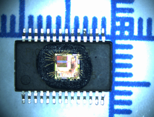
The STM32F042x4/x6 microcontrollers incorporate the high-performance
ARM® Cortex®-M0 32-bit RISC core operating at up to 48 MHz frequency, high-speed embedded memories (up to 32 Kbytes of Flash memory and 6 Kbytes of SRAM), and an extensive range of enhanced peripherals and I/Os.
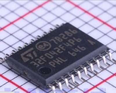
All devices offer standard communication interfaces (one I2C, two SPIs/one I2S, one HDMI CEC and two USARTs), one USB Full-speed device (crystal-less), one CAN, one 12-bit ADC, four 16-bit timers, one 32-bit timer and an advanced-control PWM timer in order to breaking off stm32f038k6 readout protection system.
защищенное восстановление программы микроконтроллера STM32F042F4 начинается с взлома бита предохранителя микропроцессора STM32F042F4 и извлечения встроенного двоичного файла из флэш-памяти микроконтроллера STM32F042F4;
The STM32F042x4/x6 microcontrollers operate in the -40 to +85 °C and -40 to +105 °C temperature ranges, from a 2.0 to 3.6 V power supply. A comprehensive set of power-saving modes allows the design of low-power applications.
 Break STM32F038K6 Microcontroller Readout Protection
Break STM32F038K6 Microcontroller Readout Protection needs to use MCU cracking technique to disable the security fuse bit of microprocessor stm32f038k6, and then replicate flash data from mcu stm32f038k6;
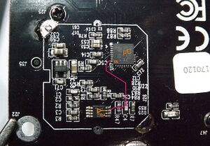
The STM32F0xx family embeds a nested vectored interrupt controller able to handle up to 32 maskable interrupt channels (not including the 16 interrupt lines of Cortex®-M0) and 4
priority levels.
- Closely coupled NVIC gives low latency interrupt processing
- Interrupt entry vector table address passed directly to the core
- Closely coupled NVIC core interface
- Allows early processing of interrupts
- Processing of late arriving higher priority interrupts
- Support for tail-chaining
- Processor state automatically saved
- Interrupt entry restored on interrupt exit with no instruction overhead
This hardware block provides flexible interrupt management features with minimal interrupt latency.
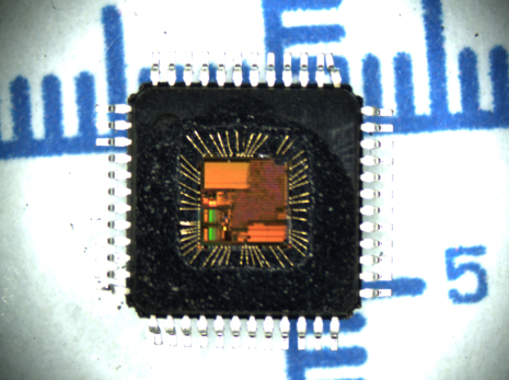
The extended interrupt/event controller consists of 24 edge detector lines used to generate interrupt/event requests and wake-up the system. Each line can be independently configured to select the trigger event (rising edge, falling edge, both) and can be masked independently.
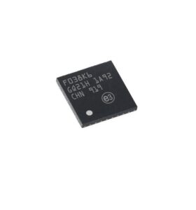
сломать защиту считывания микроконтроллера STM32F038K6 необходимо использовать технику взлома MCU, чтобы отключить бит предохранителя микропроцессора STM32F038K6, а затем реплицировать данные флэш-памяти из MCU STM32F038K6;
A pending register maintains the status of the interrupt requests. The EXTI can detect an external line with a pulse width shorter than the internal clock period. Up to 38 GPIOs can be connected to the 16 external interrupt lines.
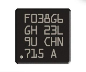
 STM32F038G6 Protective Microcomputer Attacking
STM32F038G6 Protective Microcomputer Attacking can help engineer to clone embedded flash firmware from microcontroller stm32f038g6, and then copy heximal data to new mcu stm32f038g6 for perfect functions duplication;

Each of the GPIO pins can be configured by software as output (push-pull or open-drain), as input (with or without pull-up or pull-down) or as peripheral alternate function.
Most of the GPIO pins are shared with digital or analog alternate functions. The I/O configuration can be locked if needed following a specific sequence in order to avoid spurious writing to the I/Os registers when breaking arm mcu stm32f070c6 flash memory.
The 5-channel general-purpose DMAs manage memory-to-memory, peripheral-to-memory and memory-to-peripheral transfers.
The DMA supports circular buffer management, removing the need for user code intervention when the controller reaches the end of the buffer.

Each channel is connected to dedicated hardware DMA requests, with support for software trigger on each channel. Configuration is made by software and transfer sizes between source and destination are independent in order to attack readout protection over stm32f070f6 mcu flash memory. DMA can be used with the main peripherals: SPIx, I2Sx, I2Cx, USARTx, all TIMx timers (except TIM14) and ADC.
 Recover STM32F038F6 Microcontroller Heximal Data
Recover STM32F038F6 Microcontroller Heximal Data from its flash memory, the microprocessor stm32f038f6 fuse bit will be cracked by focus ion beam technique, and then replicating firmware to new mcu stm32f038f6 for functions cloning;
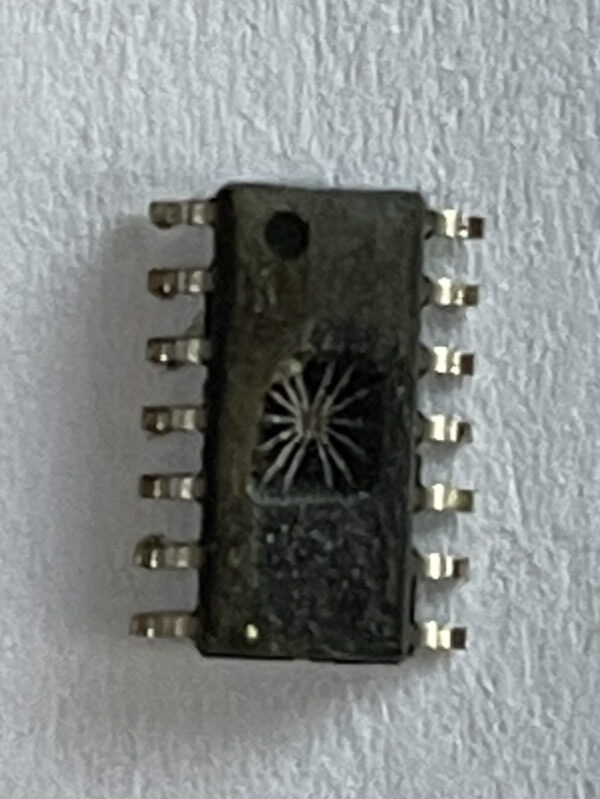
· Sleep mode
In Sleep mode, only the CPU is stopped. All peripherals continue to operate and can wake up the CPU when an interrupt/event occurs.
· Stop mode
Stop mode achieves very low power consumption while retaining the content of SRAM and registers. All clocks in the 1.8 V domain are stopped, the PLL, the HSI RC and the HSE crystal oscillators are disabled.
The device can be woken up from Stop mode by any of the EXTI lines. The EXTI line source can be one of the 16 external lines, RTC, I2C1 or USART1. USART1 and I2C1 peripherals can be configured to enable the HSI RC oscillator so as to get clock for processing incoming data when attacking stm32f038e6 microprocessor secured flash memory.
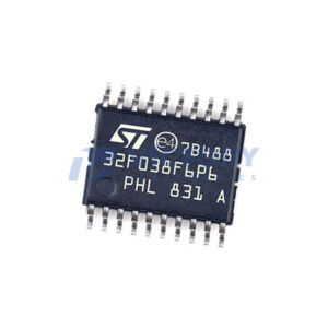
восстановить гексимальные данные микроконтроллера STM32F038F6 из его флэш-памяти, бит предохранителя микропроцессора STM32F038F6 будет взломан методом фокусировки ионного луча, а затем реплицирует прошивку на новый микроконтроллер STM32F038F6 для клонирования функций;
System clock selection is performed on startup, however the internal RC 8 MHz oscillator is selected as default CPU clock on reset. An external 4-32 MHz clock can be selected, in which case it is monitored for failure. If failure is detected, the system automatically switches back to the internal RC oscillator.
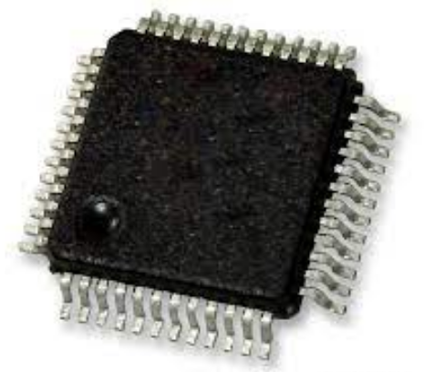
A software interrupt is generated if enabled. Similarly, full interrupt management of the PLL clock entry is available when necessary (for example on failure of an indirectly used external crystal to break stm32f038c6 microprocessor locked flash memory, resonator or oscillator). Several prescalers allow the application to configure the frequency of the AHB and the APB domains. The maximum frequency of the AHB and the APB domains is 48 MHz.
 Attack STM32F038E6 Microprocessor Secured Memory
Attack STM32F038E6 Microprocessor Secured Memory and extract locked firmware from mcu stm32f038e6 flash memory, rewrite copied heximal file to new microcontroller stm32f038e6 for processor cloning;
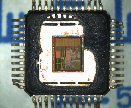
The ARM® Cortex®-M0 is a generation of ARM 32-bit RISC processors for embedded systems. It has been developed to provide a low-cost platform that meets the needs of MCU implementation, with a reduced pin count and low-power consumption, while delivering outstanding computational performance and an advanced system response to interrupts.
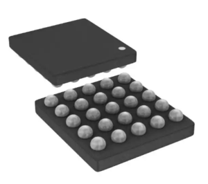
атаковать защищенную память микропроцессора STM32F038E6 и извлечь заблокированную прошивку из флэш-памяти MCU STM32F038E6, перезаписать скопированный шестигранный файл на новый микроконтроллер STM32F038E6 для клонирования процессора;
The ARM® Cortex®-M0 processors feature exceptional code-efficiency, delivering the high performance expected from an ARM core, with memory sizes usually associated with 8- and 16-bit devices when breaking stm32f030r8 microprocesor locked bits. The STM32F038x6 devices embed ARM core and are compatible with all ARM tools and software.
The device has the following features:
- 4 Kbytes of embedded SRAM accessed (read/write) at CPU clock speed with 0 wait states and featuring embedded parity checking with exception generation for fail-critical applications.
- The non-volatile memory is divided into two arrays:
- 32 Kbytes of embedded Flash memory for programs and data
- Option bytes
- The non-volatile memory is divided into two arrays:
The option bytes are used to write-protect the memory (with 4 KB granularity) and/or readout-protect the whole memory with the following options:
- Level 0: no readout protection
- Level 1: memory readout protection, the Flash memory cannot be read from or written to if either debug features are connected or boot in RAM is selected
- Level 2: chip readout protection, debug features (Cortex®-M0 serial wire) and boot in RAM selection disabled which can be attacked by readout protection removal technique;
