 Break STM32F302VD Secured Microcontroller Flash Memory
Break STM32F302VD Secured Microcontroller Flash Memory fuse bit and readout embedded firmware from locked mcu stm32f302vd, heximal file of stm32f302vd microprocessor will be duplicated from original flash memory;
The STM32F302xD/E family operates in the -40 to +85°C and -40 to +105°C temperature ranges from a 2.0 to 3.6 V power supply. A comprehensive set of power-saving mode allows the design of low-power applications.
romper STM32F302VD bit de fusible de memoria flash de microcontrolador asegurado y leer firmware integrado de MCU bloqueado STM32F302VD, el archivo hexamal del microprocesador STM32F302VD se duplicará de la memoria flash original;
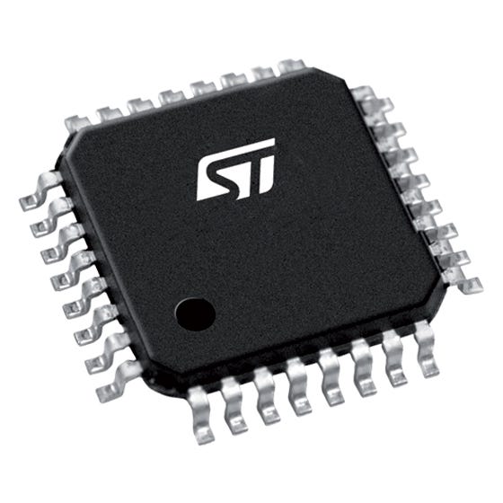
The STM32F302xD/E family offers devices in different packages ranging from 64 to 144 pins. Depending on the device chosen, different sets of peripherals are included.
The ARM® Cortex®-M4 processor with FPU is the latest generation of ARM processors for embedded systems when breaking secured microprocessor stm32f301c8 flash memory. It was developed to provide a low-cost platform that meets the needs of MCU implementation, with a reduced pin count and low-power consumption, while delivering outstanding computational performance and an advanced response to interrupts.
The ARM® Cortex®-M4 32-bit RISC processor with FPU features exceptional code- efficiency, delivering the high-performance expected from an ARM core in the memory size usually associated with 8- and 16-bit devices.
The processor supports a set of DSP instructions which allows efficient signal processing and complex algorithm execution.
STM32F302RD Locked Microprocessor Flash Firmware Copying
STM32F302RD Locked Microprocessor Flash Firmware Copying will need to disable the protection over stm32f302rd secured MCU through fuse bit by unlocking; and then extract heximal code from encrypted microcontroller stm32f302rd flash memory;
The STM32F302xD/E family is based on the high-performance ARM® Cortex®-M4 32-bit RISC core with FPU operating at a frequency of 72 MHz, and embedding a floating point unit (FPU), a memory protection unit (MPU) and an embedded trace macrocell (ETM).

The family incorporates high-speed embedded memories (512-Kbyte Flash memory, 64-Kbyte SRAM), a flexible memory controller (FSMC) for static memories (SRAM, PSRAM, NOR and NAND), and an extensive range of enhanced I/Os and peripherals connected to an AHB and two APB buses.
STM32F302RD заблокированный микропроцессор флэш-прошивки копирование прошивки потребует отключения защиты через защищенный микроконтроллер stm32f302rd через бит предохранителя путем разблокировки; а затем извлеките шестнадцатеричный код из зашифрованной флэш-памяти микроконтроллера Stm32f302rd
The devices offer two fast 12-bit ADCs (5 Msps), four comparators, two operational amplifiers, one DAC channel, a low-power RTC, up to two general-purpose 16-bit timers, one general-purpose 32-bit timer, and one timer dedicated to motor control.
They also feature standard and advanced communication interfaces: up to three I2Cs, up to four SPIs (two SPIs are with multiplexed full-duplex I2Ss), three USARTs, up to two UARTs, CAN and USB. To achieve audio class accuracy, the I2S peripherals can be clocked via an external PLL.
Attack STM32F301K8 Locked Microcontroller Readout Protection
Attack STM32F301K8 Locked Microcontroller Readout Protection and extract embedded heximal file from microprocessor stm32f301k8 flash memory, then clone flash content to new mcu stm32f301k8.
Several peripherals have direct connections between them. This allows autonomous communication between peripherals, saving CPU resources thus power supply consumption. In addition, these hardware connections allow fast and predictable latency.
System clock selection is performed on startup, however the internal RC 8 MHz oscillator is selected as default CPU clock on reset. An external 4-32 MHz clock can be selected, in which case it is monitored for failure. If failure is detected when recovering stm32f078cb microprocessor flash firmware, the system automatically switches back to the internal RC oscillator.
A software interrupt is generated if enabled. Similarly, full interrupt management of the PLL clock entry is available when necessary (for example with failure of an indirectly used external oscillator).
атака STM32F301K8 заблокированный микроконтроллер защиты от считывания и извлечение встроенного шестнадцатеричного файла из микропроцессора stm32f301k8 флэш-памяти, а затем клонирование флэш-содержимого на новый MCU stm32f301k8
Several prescalers allow to configure the AHB frequency, the high speed APB (APB2) and the low speed APB (APB1) domains. The maximum frequency of the AHB and the high speed APB domains is 72 MHz to reverse engineering stm32f078vb microcontroller program, while the maximum allowed frequency of the low speed APB domain is 36 MHz.
The advanced clock controller clocks the core and all peripherals using a single crystal or oscillator. To achieve audio class performance, an audio crystal can be used.
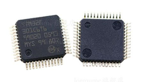
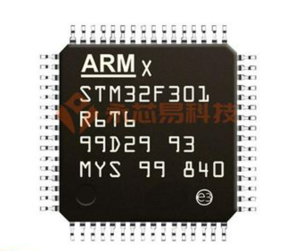
Breaking STM32F301C8 Secured Microprocessor Flash Memory
Breaking STM32F301C8 Secured Microprocessor Flash Memory and readout embedded firmware from locked microcontroller stm32f301c8, replicate flash program to new mcu stm32f301c8;

The regulator has three operation modes: main (MR), low-power (LPR), and power-down.
- The MR mode is used in the nominal regulation mode (Run)
- The LPR mode is used in Stop mode.
- The power-down mode is used in Standby mode: the regulator output is in high impedance, and the kernel circuitry is powered down thus inducing zero consumption.
The voltage regulator is always enabled after reset. It is disabled in Standby mode.
The STM32F301x6/8 supports three low-power modes to achieve the best compromise between low power consumption, short startup time and available wakeup sources:
- Sleep mode
In Sleep mode, only the CPU is stopped. All peripherals continue to operate and can wake up the CPU when an interrupt/event occurs.
- Stop mode
Stop mode achieves the lowest power consumption while retaining the content of SRAM and registers to decrypt embedded firmware from arm stm32f301c6 microprocessor. All clocks in the 1.8 V domain are stopped, the PLL, the HSI RC and the HSE crystal oscillators are disabled. The voltage regulator can also be put either in normal or in low-power mode.
взлом защищенной микропроцессорной флэш-памяти STM32F301C8 и считывание встроенного микропрограммного обеспечения с заблокированного микроконтроллера stm32f301c8, репликация флэш-программы на новый микроконтроллер stm32f301c8
The device can be woken up from Stop mode by any of the EXTI line. The EXTI line source can be one of the 16 external lines, the PVD output, the RTC alarm, COMPx, I2C or USARTx.
- Standby mode
The Standby mode is used to achieve the lowest power consumption. The internal voltage regulator is switched off so that the entire 1.8 V domain is powered off. The PLL, the HSI RC and the HSE crystal oscillators are also switched off.
After entering Standby mode, SRAM and register contents are lost except for registers in the Backup domain and Standby circuitry by restoring mcu stm32f301r8 mcu flash firmware. The device exits Standby mode when an external reset (NRST pin), an IWDG reset, a rising edge on the WKUP pin, or an RTC alarm occurs.
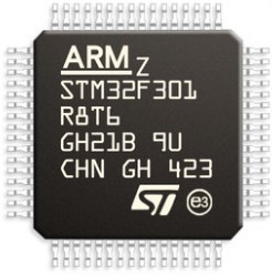
Secured STM32F301R8 MCU Flash Firmware Restoration
The first step of Secured STM32F301R8 MCU Flash Firmware Restoration is cracking the protection over stm32f301r8 microcontroller flash memory fuse bit, and then extract embedded heximal file from microprocessor stm32f301r8 flash memory;
The device has an integrated power-on reset (POR) and power-down reset (PDR) circuits. They are always active, and ensure proper operation above a threshold of 2 V. The device remains in reset mode when the monitored supply voltage is below a specified threshold, VPOR/PDR, without the need for an external reset circuit.
- The POR monitors only the VDD supply voltage. During the startup phase it is required that VDDA should arrive first and be greater than or equal to VDD.
- The PDR monitors both the VDD and VDDA supply voltages, however the VDDA power supply supervisor can be disabled (by programming a dedicated Option bit) to reduce the power consumption if the application design ensures that VDDA is higher than or equal to VDD.
The device features an embedded programmable voltage detector (PVD) that monitors the VDD power supply and compares it to the VPVD threshold by reverse engineering stm32f078r8 microcontroller flash firmware, An interrupt can be generated when VDD drops below the VPVD threshold and/or when VDD is higher than the VPVD threshold.
el primer paso de la restauración segura del firmware flash del MCU STM32F301R8 es descifrar la protección sobre el bit fusible de la memoria flash del microcontrolador STM32F301R8 y luego extraer el archivo hexamal incrustado de la memoria flash STM32F301R8 del microprocesador;
The interrupt service routine can then generate a warning message and/or put the MCU into a safe state. The PVD is enabled by software.
Encrypted STM32F301K6 Microprocessor Flash Memory Breaking
Encrypted STM32F301K6 Microprocessor Flash Memory Breaking will disable the security fuse bit of stm32f301k6 microcontroller and readout embedded heximal file from mcu stm32f301k6;
The CRC (cyclic redundancy check) calculation unit is used to get a CRC code using a configurable generator polynomial value and size.
Among other applications, CRC-based techniques are used to verify data transmission or storage integrity. In the scope of the EN/IEC 60335-1 standard, they offer a means of verifying the Flash memory integrity.
The CRC calculation unit helps compute a signature of the software during runtime by recovering stm32f301r6 microcontroller flash memory code, to be compared with a reference signature generated at linktime and stored at a given memory location.
la ruptura de la memoria flash del microprocesador STM32F301K6 cifrada deshabilitará el bit de fusible de seguridad del microcontrolador stm32f301k6 y leerá el archivo hexamal incrustado del MCU STM32F301K6;
- VSS, VDD = 2.0 to 3.6 V: external power supply for I/Os and the internal regulator. It is provided externally through VDD pins.
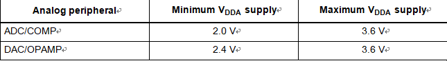
VSSA, VDDA = 2.0 to 3.6 V: external analog power supply for ADC, DAC, comparators, operational amplifier, reset blocks, RCs and PLL. The minimum voltage to be applied to VDDA differs from one analog peripheral to another.
Below Table provides the summary of the VDDA ranges for analog peripherals. The VDDA voltage level must always be greater than or equal to the VDD voltage level and must be provided first.
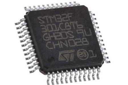
ARM STM32F301C6 Microprocessor Embedded Firmware Decryption
ARM STM32F301C6 Microprocessor Embedded Firmware Decryption can help engineer to dump flash heximal content from stm32f301c6 mcu chip, and then copy firmware file to new microcontroller stm32f301c6 which can perform the same functions;
The Arm® Cortex®-M4 processor with FPU is the latest generation of Arm processors for embedded systems. It was developed to provide a low-cost platform that meets the needs of MCU implementation, with a reduced pin count and low-power consumption, while delivering outstanding computational performance and an advanced response to interrupts.
El descifrado de firmware integrado del microprocesador ARM STM32F301C6 puede ayudar al ingeniero a volcar contenido hexamal flash del chip MCU STM32F301C6 y luego copiar el archivo de firmware al nuevo microcontrolador STM32F301C6 que puede realizar las mismas funciones;
The Arm® Cortex®-M4 32-bit RISC processor with FPU features exceptional code- efficiency, delivering the high-performance expected from an Arm core in the memory size usually associated with 8- and 16-bit devices.
The processor supports a set of DSP instructions which allow efficient signal processing and complex algorithm execution. Its single-precision FPU speeds up software development by using metalanguage development tools while avoiding saturation which can help to recovering stm32f301r6 mcu flash code. With its embedded Arm core, the STM32F301x6/8 family is compatible with all Arm tools and software.
Recover STM32F301R6 MCU Flash Memory Code
Recover STM32F301R6 MCU Flash Memory Code in the format of heximal, the firmware can be rewritten to the new microcontroller stm32f301r6, status of microprocessor stm32f301r6 will be modified by cracking microcontroller;
The STM32F301x6/8 family is based on the high-performance Arm® Cortex®-M4
32-bit RISC core operating at a frequency of up to 72 MHz and embedding a floating point unit (FPU). The family incorporates high-speed embedded memories (up to 64 Kbytes of Flash memory, 16 Kbytes of SRAM), and an extensive range of enhanced I/Os and peripherals connected to two APB buses.
The devices offer a fast 12-bit ADC (5 Msps), three comparators, an operational amplifier, up to 18 capacitive sensing channels, one DAC channel, a low-power RTC, one general- purpose 32-bit timer, one timer dedicated to motor control by reverse engineering stm32f078r8 mcu flash, and up to three general-purpose 16-bit timers, and one timer to drive the DAC. They also feature standard and advanced communication interfaces: three I2Cs, up to three USARTs, up to two SPIs with multiplexed full-duplex I2S, and an infrared transmitter.
recuperar el código de memoria flash STM32F301R6 MCU en el formato de hexadecimal, el firmware se puede reescribir en el nuevo microcontrolador STM32F301R6, el estado del microprocesador STM32F301R6 se modificará al descifrar el microcontrolador
The STM32F301x6/8 family operates in the –40 to +85°C and –40 to +105°C temperature ranges from at a 2.0 to 3.6 V power supply. A comprehensive set of power-saving mode allows the design of low-power applications which is similar with the process of breaking microcontroller stm32f042g4 flash memory. The STM32F301x6/8 family offers devices in 32-, 48-, 49- and 64-pin packages. The set of included peripherals changes with the device chosen.
Microcontroller STM32F048T6 Flash Heximal Cloning
Microcontroller STM32F048T6 Flash Heximal Cloning after mcu stm32f048t6 source code extracting, the status of microprocessor stm32f048t6 will be reset by decrypting;
At startup, the boot pin and boot selector option bits are used to select one of the three boot options:
- boot from User Flash memory
- boot from System Memory
- boot from embedded SRAM
The boot pin is shared with the standard GPIO and can be disabled through the boot selector option bits. The boot loader is located in System Memory. It is used to reprogram the Flash memory by using USART on pins PA14/PA15 or PA9/PA10 or I2C on pins PB6/PB7 or through the USB DFU interface.
The CRC (cyclic redundancy check) calculation unit is used to get a CRC code from a 32-bit data word and a CRC-32 (Ethernet) polynomial by recovering smt32f038f6 microcontroller heximal file. Among other applications, CRC-based techniques are used to verify data transmission or storage integrity.
In the scope of the EN/IEC 60335-1 standard, they offer a means of verifying the Flash memory integrity. The CRC calculation unit helps compute a signature of the software during runtime, to be compared with a reference signature generated at link- time and stored at a given memory location.
Restoring STM32F048G6 Secured MCU Flash Program
Restoring STM32F048G6 Secured MCU Flash Program needs to unlock microprocessor stm32f048g6 locked fuse bit, and copy firmware heximal to new microcontroller stm32f048g6 for mcu cloning;
The ARM® Cortex®-M0 is a generation of ARM 32-bit RISC processors for embedded systems. It has been developed to provide a low-cost platform that meets the needs of MCU implementation, with a reduced pin count and low-power consumption, while delivering outstanding computational performance and an advanced system response to interrupts.
The ARM® Cortex®-M0 processors feature exceptional code-efficiency, delivering the high performance expected from an ARM core, with memory sizes usually associated with 8- and 16-bit devices by stm32f031c6 microprocessor flash cracking. The STM32F048x6 devices embed ARM core and are compatible with all ARM tools and software.
The device has the following features:
- 6 Kbytes of embedded SRAM accessed (read/write) at CPU clock speed with 0 wait states and featuring embedded parity checking with exception generation for fail-critical applications.
- The non-volatile memory is divided into two arrays:
- 32 Kbytes of embedded Flash memory for programs and data
- Option bytes
- The non-volatile memory is divided into two arrays:
The option bytes are used to write-protect the memory (with 4 KB granularity) and/or readout-protect the whole memory with the following options:
- Level 0: no readout protection
- Level 1: memory readout protection, the Flash memory cannot be read from or written to if either debug features are connected or boot in RAM is selected
- Level 2: chip readout protection, debug features (Cortex®-M0 serial wire) and boot in RAM selection disabled