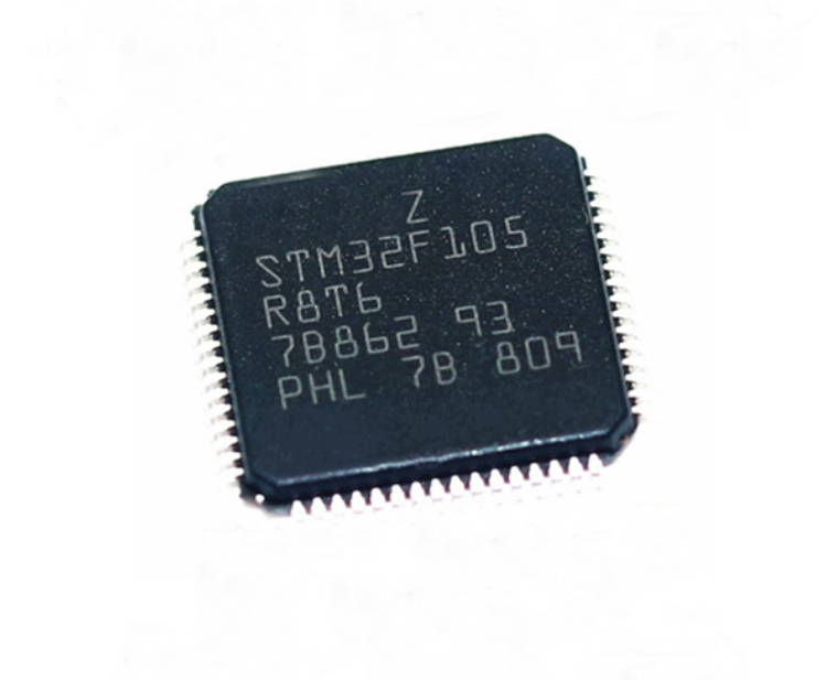
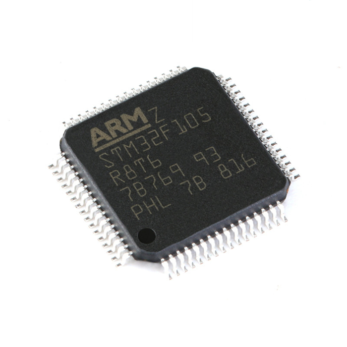
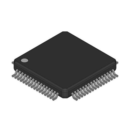
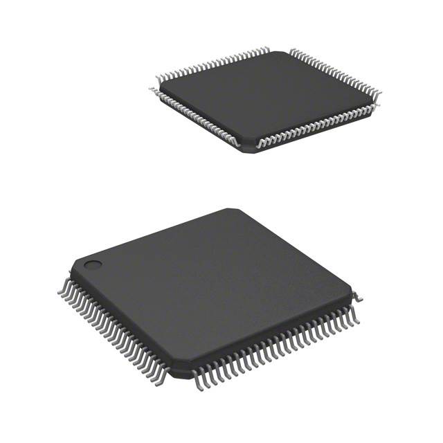
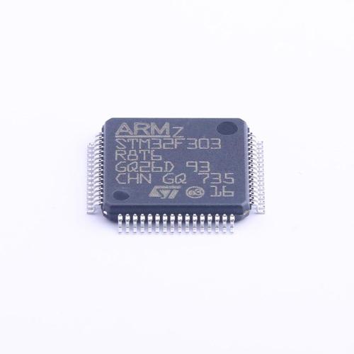
 Unlock STM32F105R8 Secured Microprocessor Flash Memory
Unlock STM32F105R8 Secured Microprocessor Flash Memory and extract embedded firmware from locked MCU STM32F105R8, and then copy heximal file to new stm32f105r8 microcontroller;

The STM32F050xx family supports three low-power modes to achieve the best compromise between low power consumption, short startup time and available wakeup sources:
● Sleep mode
In Sleep mode, only the CPU is stopped. All peripherals continue to operate and can wake up the CPU when an interrupt/event occurs.
● Stop mode
Stop mode achieves very low power consumption while retaining the content of SRAM and registers. All clocks in the 1.8 V domain are stopped, the PLL, the HSI RC and the HSE crystal oscillators are disabled in order to replicating embedded flash program from stm32f105r8 mcu. The voltage regulator can also be put either in normal or in low power mode.
crack locked stm32f105r8 MCU fuse bit and restore embedded heximal program file from flash memory of stm32f105r8 MCU
The device can be woken up from Stop mode by any of the EXTI lines. The EXTI line source can be one of the 16 external lines, the PVD output, RTC alarm, I2C1 or USART1.
The I2C1 and the USART1 can be configured to enable the HSI RC oscillator for processing incoming data. If this is used, the voltage regulator should not be put in the low-power mode but kept in normal mode.
● Standby mode
The Standby mode is used to achieve the lowest power consumption. The internal voltage regulator is switched off so that the entire 1.8 V domain is powered off. The PLL, the HSI RC and the HSE crystal oscillators are also switched off. After entering Standby mode for the sake of restoring arm microcontroller stm32f103c4 flash binary, SRAM and register contents are lost except for registers in the Backup domain and Standby circuitry.
attack encrypted stm32f105r8t6 microcontroller protection and copy heximal program software from flash memory
The device exits Standby mode when an external reset (NRST pin), a IWDG reset, a rising edge on the WKUP pins, or an RTC alarm occurs.
Note: The RTC, the IWDG, and the corresponding clock sources are not stopped by entering Stop or Standby mode.
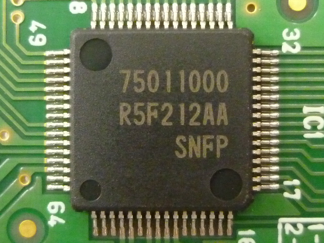
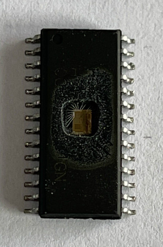
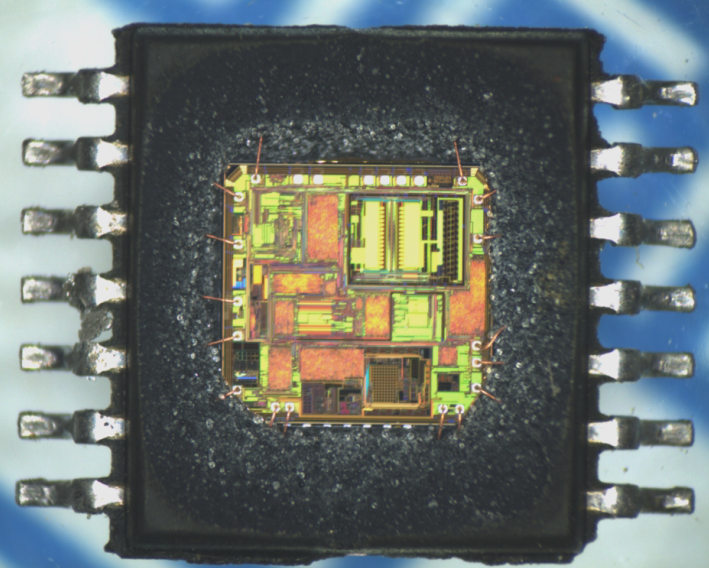
Renesas Locked R5F212AASDFP Memory Data Copying
Renesas Locked R5F212AASDFP Memory Data Copying will need to decrypt renesas MCU R5F212AASDFP flash memory content, copy software to new microprocessor R5F212AASDFP;
R0 is a 16-bit register for transfer, arithmetic, and logic operations. The same applies to R1 to R3. R0 can be split into high-order bits (R0H) and low-order bits (R0L) to be used separately as 8-bit data registers.
R1H and R1L are analogous to R0H and R0L. R2 can be combined with R0 and used as a 32-bit data register (R2R0). R3R1 is analogous to R2R0.
A0 is a 16-bit register for address register indirect addressing and address register relative addressing. It is also used for transfer, arithmetic, and logic operations. A1 is analogous to A0. A1 can be combined with A0 and as a 32- bit address register (A1A0).
Renesas bloqueado R5F212AASDFP cópia de dados de memória precisará descriptografar renesas MCU R5F212AASDFP conteúdo de memória flash, copiar o software para o novo microprocessador R5F212AASDFP;
FB is a 16-bit register for FB relative addressing.
INTB is a 20-bit register that indicates the start address of an interrupt vector table.
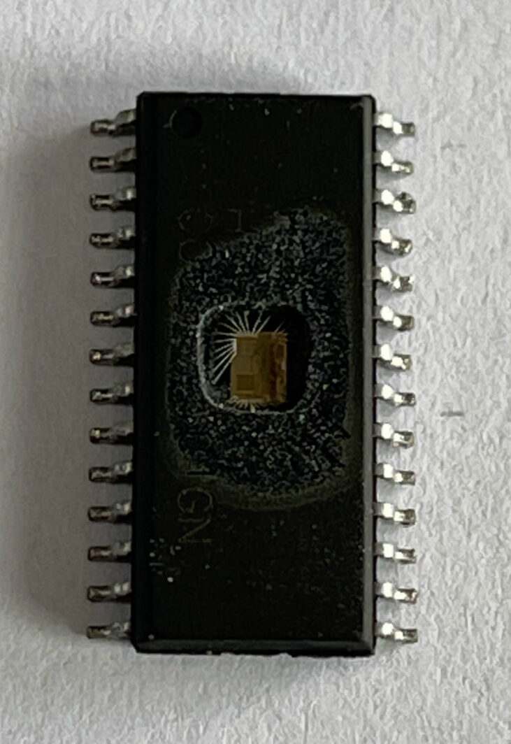
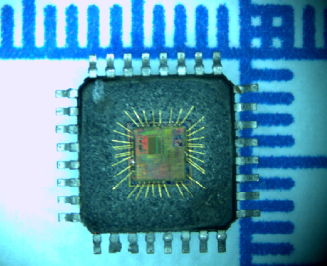
Dump Renesas R5F212A7SDFA Protect MCU Flash Program
Dump Renesas R5F212A7SDFA Protect MCU Flash Program needs to know its internal structure and programming mechanism, extract its embedded firmware from R5F212A7SDFA microcontroller, and clone heximal file to new microprocessor R5F212A7SDFA;

R8C/Tiny series core
- Number of fundamental instructions: 89
- Minimum instruction execution time:
50 ns (f(XIN) = 20 MHz, VCC = 3.0 to 5.5 V)
100 ns (f(XIN) = 10 MHz, VCC = 2.7 to 5.5 V)
200 ns (f(XIN) = 5 MHz, VCC = 2.2 to 5.5 V)
- Multiplier: 16 bits × 16 bits ® 32 bits
- Multiply-accumulate instruction: 16 bits × 16 bits + 32 bits ® 32 bits
Operation mode: Single-chip mode (address space: 1 Mbyte)
3 circuits: XIN clock oscillation circuit (with on-chip feedback resistor) to breaking mcu R5F2L388 flash firmware,
On-chip oscillator (high-speed, low-speed)
(high-speed on-chip oscillator has a frequency adjustment function), XCIN clock oscillation circuit (32 kHz)
- Oscillation stop detection: XIN clock oscillation stop detection function
- Frequency divider circuit: Dividing selectable 1, 2, 4, 8, and 16
- Low power consumption modes:
Standard operating mode (high-speed clock, low-speed clock, high-speed on-chip oscillator, low-speed on-chip oscillator), wait mode, stop mode.
dump Renesas R5F212A7SDFA protegido MCU flash programa precisa conhecer sua estrutura interna e mecanismo de programação, extrair seu firmware incorporado do microcontrolador R5F212A7SDFA e clonar o arquivo heximal para o novo microprocessador R5F212A7SDFA
- External: 5 sources, Internal: 23 sources, Software: 4 sources
Priority levels: 7 levels
8 bits × 1 (with 8-bit prescaler)
Timer mode (period timer), pulse output mode (output level inverted every period), event counter mode, pulse width measurement mode, pulse period measurement mode.
8 bits × 1 (with 8-bit prescaler)
Timer mode (period timer), programmable waveform generation mode (PWM output), programmable one-shot generation mode, programmable wait one- shot generation mode
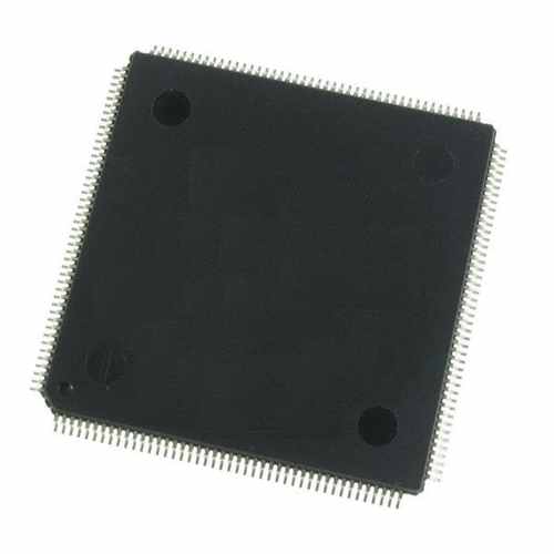
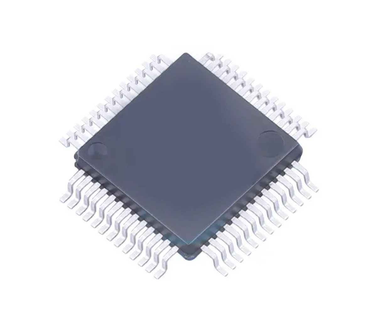
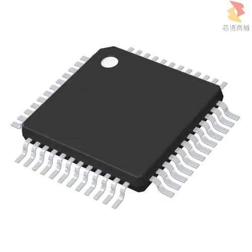
Reverse Engineer STM32F050K4 Microprocessor
Reverse Engineer STM32F050K4 Microprocessor Protection over flash memory, and break stm32f050k4 secured mcu firmware file, extract source code from stm32f050k4 microprocessor flash memory;
The device has the following features:
- 4 Kbytes of embedded SRAM accessed (read/write) at CPU clock speed with 0 wait states and featuring embedded parity checking with exception generation for fail-critical applications by restoring microcomputer stm32f072cb firmware file.
- The non-volatile memory is divided into two arrays:
- 16 to 32 Kbytes of embedded Flash memory for programs and data
- Option bytes
- The non-volatile memory is divided into two arrays:
The option bytes are used to write-protect the memory (with 4 KB granularity) and/or readout-protect the whole memory with the following options:
- Level 0: no readout protection
- Level 1: memory readout protection, the Flash memory cannot be read from or written to if either debug features are connected or boot in RAM is selected
Level 2: chip readout protection, debug features (Cortex-M0 serial wire) and boot in RAM selection disabled.
engenharia reversa STM32F050K4 proteção do microprocessador sobre memória flash, e quebrar stm32f050k4 arquivo de firmware mcu seguro, extrair o código-fonte da memória flash do microprocessador stm32f050k4
At startup, the boot pin and boot selector option bit are used to select one of three boot options:
- Boot from User Flash
- Boot from System Memory
- Boot from embedded SRAM
The boot loader is located in System Memory. It is used to reprogram the Flash memory by using USART1.
Breaking MCU STM32F050G4 Flash Memory
Breaking MCU STM32F050G4 Flash Memory and extract embedded heximal file out from microcontroller stm32f050g4, copy firmware from original microprocessor stm32f050g4 flash memory;
These features make the STM32F050xx microcontroller family suitable for a wide range of applications such as control application and user interfaces, handheld equipment, A/V receivers and digital TV, PC peripherals, gaming and GPS platforms, industrial applications, PLCs, inverters, printers, scanners, alarm systems, video intercoms, and HVACs.
The ARM Cortex™-M0 processor is the latest generation of ARM processors for embedded systems which will be used for reverse engineering stm32f078vb microcontroller. It has been developed to provide a low-cost platform that meets the needs of MCU implementation, with a reduced pin count and low-power consumption, while delivering outstanding computational performance and an advanced system response to interrupts.
quebrando a memória flash MCU STM32F050G4 e extrair arquivo heximal embutido do microcontrolador stm32f050g4, copiar firmware do microprocessador original stm32f050g4 memória flash;
The ARM Cortex™-M0 32-bit RISC processor features exceptional code-efficiency, delivering the high-performance expected from an ARM core in the memory size usually associated with 8- and 16-bit devices for recovering stm32f051c4 microcontroller flash binary. The STM32F050xx family has an embedded ARM core and is therefore compatible with all ARM tools and software.
Locked STM32F050F4 Microcontroller Source Code Extraction
Crack stm32f050f4 secured mcu locked fuse bit by focus ion beam, the whole microprocessor embedded heximal copying job can be done through Locked STM32F050F4 Microcontroller Source Code Extraction.
The STM32F050xx family incorporates the high-performance ARM Cortex™-M0 32-bit RISC core operating at a 48 MHz maximum frequency, high-speed embedded memories (Flash memory up to 32 Kbytes and SRAM up to 4 Kbytes), and an extensive range of enhanced peripherals and I/Os.
All devices offer standard communication interfaces (one I2C, one SPI, one I2S, and one USART), one 12-bit ADC, up to five general-purpose 16-bit timers, a 32-bit timer and an advanced-control PWM timer to break stm32f071rb microcontroller locked bits.
The STM32F050xx family operates in the -40 to +85 °C and -40 to +105 °C temperature ranges, from a 2.0 to 3.6 V power supply. A comprehensive set of power-saving modes allows the design of low-power applications.
crack stm32f050f4 seguro mcu bloqueado fusível bit por feixe de íons de foco, todo o trabalho de cópia heximal embutida microprocessador pode ser feito através de Extração de Código Fonte do Microcontrolador Bloqueado STM32F050F4.
The STM32F050xx family includes devices in five different packages ranging from 20 pins to 48 pins. Depending on the device chosen and reverse engineer stm32f071r8 microcomputer flash program, different sets of peripherals are included. An overview of the complete range of peripherals proposed in this family is provided.
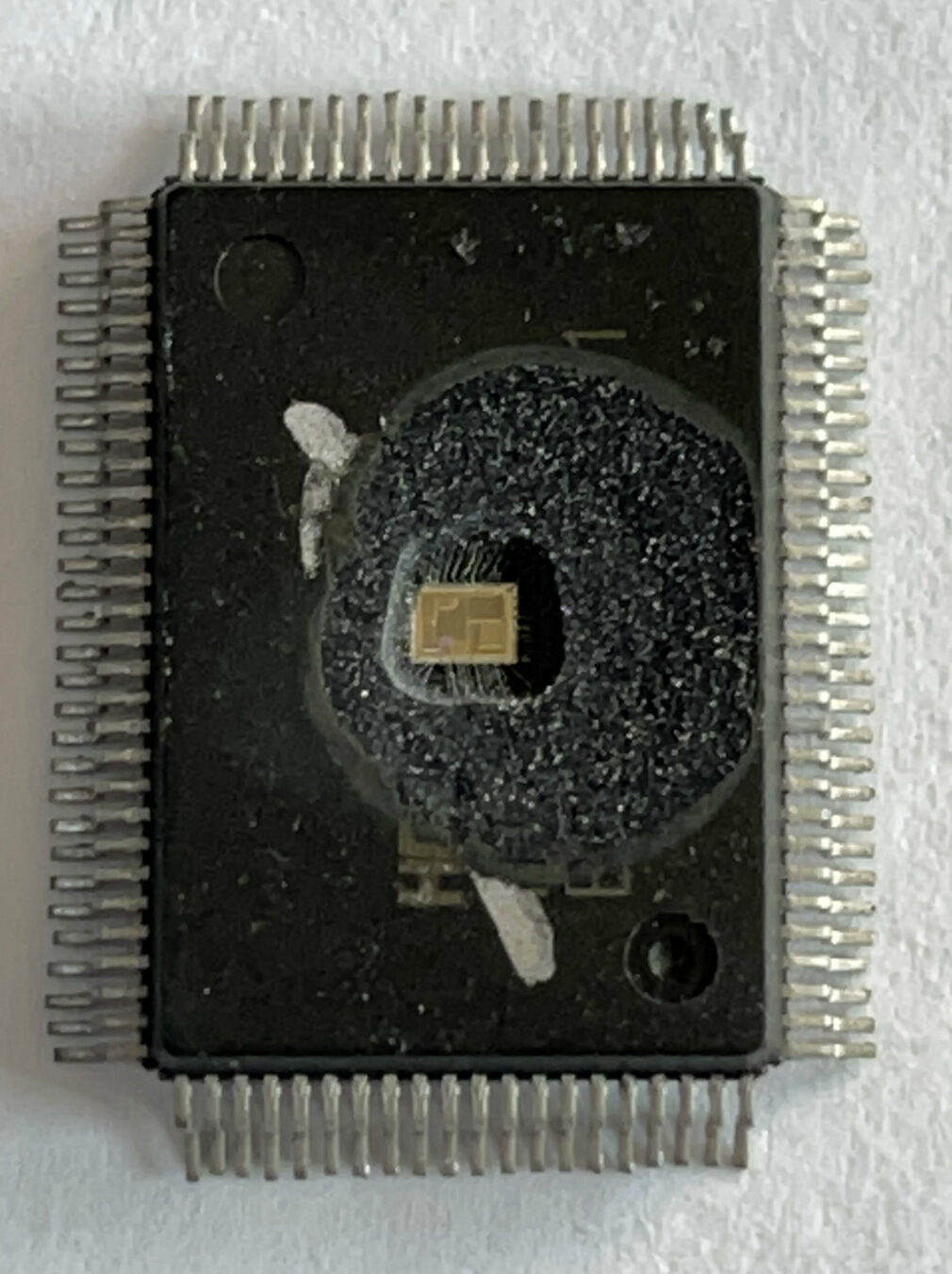
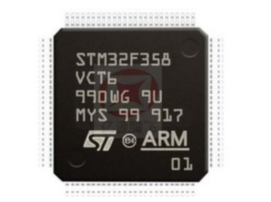
STM32F358VC Protected Microcontroller Flash Memory Breaking
STM32F358VC Protected Microcontroller Flash Memory Breaking will be able to copy embedded firmware from microprocessor stm32f358vc flash firmware, and then readout flash code from locked stm32f358vc mcu;
The memory protection unit (MPU) is used to separate the processing of tasks from the data protection. The MPU can manage up to 8 protection areas that can all be further divided up into 8 subareas. The protection area sizes are between 32 bytes and the whole 4 gigabytes of addressable memory.
The memory protection unit is especially helpful for applications where some critical or certified code has to be protected against the misbehavior of other tasks to attack stm32f303ze locked microcontroller locked bits. It is usually managed by an RTOS (real-time operating system).
If a program accesses a memory location that is prohibited by the MPU, the RTOS can detect it and take action. In an RTOS environment, the kernel can dynamically update the MPU area setting, based on the process to be executed. The MPU is optional and can be bypassed for applications that do not need it.
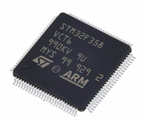
STM32F358VC protegido microcontrolador quebra de memória flash será capaz de copiar firmware incorporado do microprocessador stm32f358vc firmware flash e, em seguida, ler o código flash de stm32f358vc bloqueado mcu;
All STM32F358xC devices feature up to 256 Kbytes of embedded Flash memory available for storing programs and data. The Flash memory access time is adjusted to the CPU clock frequency in the process of stm32f358cc secured mcu flash memory breaking, (0 wait state from 0 to 24 MHz, 1 wait state from 24 to 48 MHz and 2 wait states above).
STM32F358RC Locked Microprocessor Flash Heximal Restoration
STM32F358RC Locked Microprocessor Flash Heximal Restoration firstly need to crack secured mcu stm32f358rc flash memory, then extract embedded firmware from encrypted microcontroller stm32f358rc flash memory;
The ARM® Cortex®-M4 processor with FPU is the latest generation of ARM processors for embedded systems. It was developed to provide a low-cost platform that meets the needs of MCU implementation when recovering stm32f303zd embedded firmware from microcontroller flash memory, with a reduced pin count and low-power consumption, while delivering outstanding computational performance and an advanced response to interrupts.
The ARM® Cortex®-M4 32-bit RISC processor with FPU features exceptional code- efficiency, delivering the high-performance expected from an ARM core in the memory size usually associated with 8- and 16-bit devices. The processor supports a set of DSP instructions which allow efficient signal processing and complex algorithm execution to break stm32f302ve microprocessor flash memory.
STM32F358RC bloqueado microprocessador flash restauração heximal primeiro precisa quebrar a memória flash mcu stm32f358rc segura, em seguida, extrair firmware incorporado do microcontrolador criptografado stm32f358rc memória flash
Its single precision FPU speeds up software development by using metalanguage development tools, while avoiding saturation. With its embedded ARM core, the STM32F358xC family is compatible with all ARM tools and software.
STM32F358CC Secured MCU Flash Memory Breaking
STM32F358CC Secured MCU Flash Memory Breaking means the locked bits which has been embedded on the microcontroller stm32f358cc will be cracked, and then copy the flash program to new microprocessor stm32f358cc;
The STM32F358xC family is based on the high-performance ARM® Cortex®-M4 32-bit RISC core with FPU operating at a frequency of up to 72 MHz, and embedding a floating point unit (FPU), a memory protection unit (MPU) and an embedded trace macrocell (ETM).
The family incorporates high-speed embedded memories (up to 256 Kbytes of Flash memory, up to 48 Kbytes of SRAM) and an extensive range of enhanced I/Os and peripherals connected to two APB buses when attacking stm32f303ze microcontroller flash memory locked bits.
The devices offer up to four fast 12-bit ADCs (5 Msps), up to seven comparators, up to four operational amplifiers, up to two DAC channels, a low-power RTC, up to five general- purpose 16-bit timers, one general-purpose 32-bit timer, and two timers dedicated to motor control.
STM32F358CC seguro MCU quebra de memória significa que os bits bloqueados que foram incorporados no microcontrolador stm32f358cc serão quebrados e, em seguida, copie o programa flash para o novo microprocessador stm32f358cc
They also feature standard and advanced communication interfaces: up to two I2Cs, up to three SPIs (two SPIs are with multiplexed full-duplex I2Ss on STM32F358xC devices), three USARTs, up to two UARTs, and CAN which can be used for reverse engineering stm32f303ve microprocessor flash memory, To achieve audio class accuracy, the I2S peripherals can be clocked via an external PLL.
Attack STM32F303ZE Microcontroller Locked Bit
Attack STM32F3030ZE Microcontroller Locked Bit and restore embedded firmware from secured mcu stm32f303ze flash memory, then copy secured mcu stm32f303ze flash program to new microprocessor units as cloned units;
STM32F303xD/E devices feature 80 Kbytes of embedded SRAM with hardware parity check. The memory can be accessed in read/write at CPU clock speed with 0 wait states, allowing the CPU to achieve 90 Dhrystone MIPS at 72 MHz (when running code from the CCM (Core Coupled Memory) RAM).
16 Kbytes of CCM SRAM mapped on both instruction and data bus, used to execute critical routines or to access data by breaking stm32f302zd secured microcontroller flash memory (parity check on all of CCM SRAM).
ataque STM32F3030ZE microcontrolador bloqueado bit e restaurar firmware incorporado de memória flash mcu stm32f303ze segura, em seguida, copiar seguro mcu stm32f303ze programa flash para novas unidades de microprocessador como unidades clonadas
64 Kbytes of SRAM mapped on the data bus (parity check on first 32 Kbytes of SRAM).
At startup, Boot0 pin and Boot1 option bit are used to select one of three boot options:
Boot from user Flash
Boot from system memory
Boot from embedded SRAM
The boot loader is located in the system memory. It is used to reprogram the Flash memory by using USART1 (PA9/PA10), USART2 (PA2/PA3) or USB (PA11/PA12) through DFU (device firmware upgrade).
The CRC (cyclic redundancy check) calculation unit is used to get a CRC code using a configurable generator polynomial value and size. Among other applications when reverse stm32f302re microcontroller flash program code, CRC-based techniques are used to verify data transmission or storage integrity.
In the scope of the EN/IEC 60335-1 standard, they offer a means of verifying the Flash memory integrity. The CRC calculation unit helps compute a signature of the software during runtime, to be compared with a reference signature generated at linktime and stored at a given memory location.