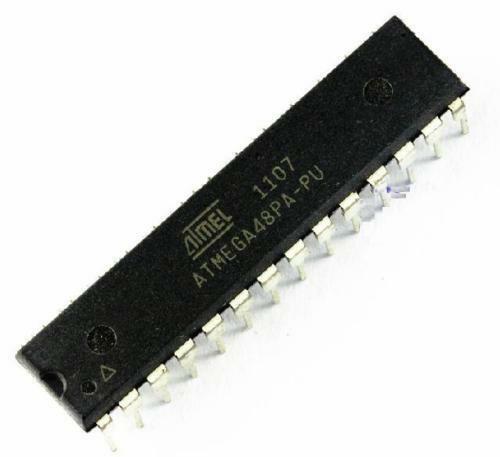
 Reverse engineering MCU ATMEGA48PV Code
We can Reverse engineering MCU ATMEGA48PV Code, please view the MCU ATMEGA48PV features for your reference:
crack atmega48pa mcu fuse bit and readout microprocessor flash memory in the format of binary or heximal
When a change of the logic level (an event) occurs on the Input Capture Pin (ICPn), alternatively on the analog Comparator output (ACO), and this change confirms to the setting of the edge detector, a capture will be triggered.
When a capture is triggered, the 16-bit value of the counter (TCNTn) is written to the Input Capture Register (ICRn). The Input Capture Flag (ICFn) is set at the same system clock as the TCNTn value is copied into ICRn Register.
If enabled (TICIEn = 1), the input capture flag generates an input capture interrupt. The ICFn flag is automatically cleared when the interrupt is executed.
Alternatively the ICFn flag can be cleared by software by writing a logical one to its I/O bit location. Reading the 16-bit value in the Input Capture Register (ICRn) is done by first reading the low byte (ICRnL) and then the high byte (ICRnH).
When the low byte is read the high byte is copied into the high byte Temporary Register (TEMP). When the CPU reads the ICRnH I/O location it will access the TEMP Register.
break atmega48pa microcomputer protection
The ICRn Register can only be written when using a Waveform Generation mode that utilizes the ICRn Register for defining the counter’s TOP value. In these cases the Waveform Generation mode (WGMn3:0) bits must be set before the TOP value can be written to the ICRn Register if Reverse engineering MCU atmega324pv Code.
When writing the ICRn Register the high byte must be written to the ICRnH I/O location before the low byte is written to ICRnL. The main trigger source for the input capture unit is the Input Capture Pin (ICPn). Timer/Counter1 can alternatively use the analog comparator output as trigger source for the input capture unit before break microcontroller atmega324a MCU Code.
The Analog Comparator is selected as trigger source by setting the analog Comparator Input Capture (ACIC) bit in the Analog Comparator Control and Status Register (ACSR). Be aware that changing trigger source can trigger a capture;
The input capture flag must therefore be cleared after the change. Both the Input Capture Pin (ICPn) and the Analog Comparator output (ACO) inputs are sampled using the same technique as for the Tn pin. The edge detector is also identical. However, when the noise canceler is enabled, additional logic is inserted before the edge detector, which increases the delay by four system clock cycles. Note that the input of the noise canceler and edge detector is always enabled unless the Timer/Counter is set in a Waveform Generation mode that uses ICRn to define TOP.
Break Microprocessor ATMEGA48P Flash
We can Break Microprocessor ATMEGA48P Flash, please view the Microprocessor ATMEGA48P features for your reference:
The Timer/Counter can be clocked by an internal or an external clock source. The clock source is selected by the Clock Select logic which is controlled by the Clock Select (CSn2:0) bits located in the Timer/Counter control Register B (TCCRnB) when break microprocessor flash.
The main part of the 16-bit Timer/Counter is the programmable 16-bit bi-directional counter unit. Figure 50 shows a block diagram of the counter and its surroundings if break microprocessor flash.
The 16-bit counter is mapped into two 8-bit I/O memory locations: Counter High (TCNTnH) containing the upper eight bits of the counter, and Counter Low (TCNTnL) containing the lower eight bits. The TCNTnH Register can only be indirectly accessed by the CPU before break microprocessor flash.
When the CPU does an access to the TCNTnH I/O location, the CPU accesses the high byte temporary register (TEMP). The temporary register is updated with the TCNTnH value when the TCNTnL is read, and TCNTnH is updated with the temporary register value when TCNTnL is written after break microprocessor flash.
This allows the CPU to read or write the entire 16-bit counter value within one clock cycle via the 8-bit data bus. It is important to notice that there are special cases of writing to the TCNTn Register when the counter is counting that will give unpredictable results when break microprocessor flash.
The special cases are described in the sections where they are of importance. Depending on the mode of operation used, the counter is cleared, incremented, or decremented at each timer clock (clkTn) if break microprocessor flash.
The clkTn can be generated from an external or internal clock source, selected by the Clock Select bits (CSn2:0). When no clock source is selected (CSn2:0 = 0) the timer is stopped. However, the TCNTn value can be accessed by the CPU, independent of whether clkTn is present or not before break microprocessor flash.
A CPU write overrides (has priority over) all counter clear or count operations. The counting sequence is determined by the setting of the Waveform Generation mode bits (WGMn3:0) located in the Timer/Counter Control Registers A and B (TCCRnA and TCCRnB) after break microprocessor flash.
There are close connections between how the counter behaves (counts) and how waveforms are generated on the Output Compare outputs OCnx. For more details about advanced counting sequences and waveform generation, see “Modes of Operation” on page 147 when break microprocessor flash.
The Timer/Counter Overflow Flag (TOVn) is set according to the mode of operation selected by the WGMn3:0 bits. TOVn can be used for generating a CPU interrupt if break microprocessor flash.
The Timer/Counter incorporates an input capture unit that can capture external events and give them a time-stamp indicating time of occurrence before break microprocessor flash.
The external signal indicating an event, or multiple events, can be applied via the ICPn pin or alternatively, for the Timer/Counter1 only, via the Analog Comparator unit. The time-stamps can then be used to calculate frequency, duty-cycle, and other features of the signal applied. Alternatively the time-stamps can be used for creating a log of the events after break microprocessor flash.
The Input Capture unit is illustrated by the block diagram shown in Figure 51. The elements of the block diagram that are not directly a part of the input capture unit are gray shaded. The small “n” in register and bit names indicates the Timer/Counter number.
Recover MCU Microchip CF755 Dump
Recover MCU Microchip CF755 Dump
We can recover MCU Microchip CF755 Dump, please view the PIC MCU features for your reference:
The PIC16C5X from Microchip Technology of recover MCU is a family of low-cost, high performance, 8-bit, fully static, EPROM/ ROM-based CMOS microcontrollers. It employs a RISC architecture with only 33 single word/single cycle instructions. All instructions are single cycle (200 ns) except for program branches which take two cycles. The PIC16C5X delivers performance an order of magnitude higher than its competitors in the same price category. The 12-bit wide instructions are highly symmetrical resulting in 2:1 code compression over other 8-bit microcontrollers in its class. The easy to use and easy to remember instruction set reduces development time significantly for recover MCU.
The PIC16C5X products are equipped with special features that reduce system cost and power requirements.
The Power-On Reset (POR) and Device Reset Timer (DRT) eliminate the need for external reset circuitry.
There are four oscillator configurations to choose from, including the power-saving LP (Low Power) oscillator and cost saving RC oscillator. Power saving SLEEP mode, Watchdog Timer and code protection features improve system cost, power and reliability.
The UV erasable CERDIP packaged versions are ideal for code development, while the cost-effective One Time Programmable (OTP) versions are suitable for production in any volume. The customer can take full advantage of Microchip’s price leadership in OTP microcontrollers while benefiting from the OTP’s flexibility after PIC MCU recovery.
The PIC16C5X products are supported by a full-featured macro assembler, a software simulator, an in-circuit emulator, a ‘C’ compiler, fuzzy logic support tools, a low-cost development programmer, and a full featured programmer. All the tools are supported on IBM® PC and compatible machines.
The PIC16C5X series fits perfectly in applications ranging from high-speed automotive and appliance motor control to low-power remote transmitters/receivers, pointing devices and telecom processors. The EPROM technology makes customizing application programs (transmitter codes, motor speeds, receiver frequencies, etc.) extremely fast and convenient. The small footprint packages, for through hole or surface mounting, make this microcontroller series perfect for applications with space limitations. Low-cost, low-power, high performance, ease of use and I/O flexibility make the PIC MCU recovery.
PIC16C5X series very versatile even in areas where no microcontroller use has been considered before (e.g., timer functions, replacement of “glue” logic in larger systems, coprocessor applications). tures that reduce system cost and power requirements.
The Power-On Reset (POR) and Device Reset Timer (DRT) eliminate the need for external reset circuitry when recover mcu.
There are four oscillator configurations to choose from, including the power-saving LP (Low Power) oscillator and cost saving RC oscillator. Power saving SLEEP mode, Watchdog Timer and code protection features improve system cost, power and reliability.
The UV erasable CERDIP packaged versions are ideal for code development, while the cost-effective One Time Programmable (OTP) versions are suitable for production in any volume. The customer can take full advantage of Microchip’s price leadership in OTP microcontrollers while benefiting from the OTP’s flexibility for pic mcu crack.
The PIC16C5X products are supported by a full-featured macro assembler, a software simulator, an in-circuit emulator, a ‘C’ compiler, fuzzy logic support tools, a low-cost development programmer, and a full featured programmer. All the tools are supported on IBM® PC and compatible machines.
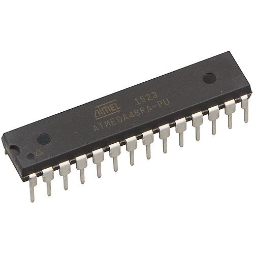
Reverse Engineering MCU ATMEGA48P Program
Reverse Engineering MCU ATMEGA48P Program from flash memory and copy heximal program to new microcontroller atmega48p secured chipset;
Not all 16-bit accesses uses the Temporary Register for the high byte. Reading the OCRnA/B/C 16-bit registers does not involve using the Temporary Register, To do a 16-bit write, the high byte must be written before the low byte. For a 16-bit read, the low byte must be read before the high byte.
The following code examples show how to access the 16-bit timer registers assuming that no interrupts updates the temporary register. The same principle can be used directly for accessing the OCRnA/B/C and ICRn Registers. Note that when using “C”, the compiler handles the 16-bit access.
unlock encrypted atmega48pv microcontroller protective system and dump embedded heximal file from flash memory
The assembly code example returns the TCNTn value in the r17:r16 register pair. It is important to notice that accessing 16-bit registers are atomic operations when breaking microcontroller atmega48p atmel avr chip fuse bit. If an interrupt occurs between the two instructions accessing the 16-bit register, and the interrupt code updates the temporary register by accessing the same or any other of the 16-bit Timer Registers, then the result of the access outside the interrupt will be corrupted.
crack secured mcu atmega48v fuse bit and extract embedded heximal file from flash memory
Therefore, when both the main code and the interrupt code update the temporary register, the main code must disable the interrupts during the 16-bit access after readout microcontroller atmega48pa binary file and heximal from eeprom and flash memory. The following code examples show how to do an atomic read of the TCNTn Register contents. Reading any of the OCRnA/B/C or ICRn Registers can be done by using the same principle.
If writing to more than one 16-bit register where the high byte is the same for all registers written, then the high byte only needs to be written once. However, note that the same rule of atomic operation described previously also applies in this case.
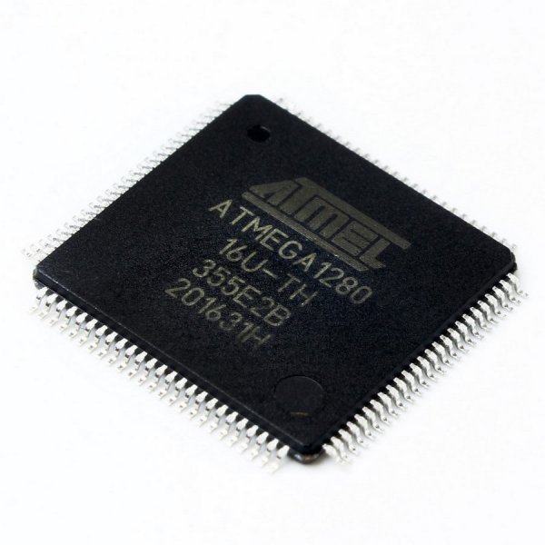
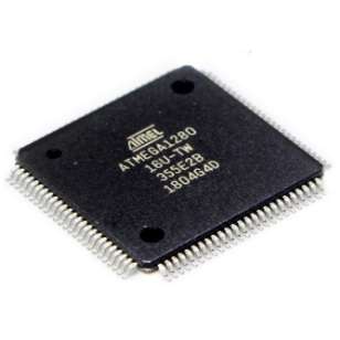
Recover Microprocessor ATMEGA1280PA Flash
Recover Microprocessor ATMEGA1280PA Flash memory data file and copy the heximal program and data to new microcontroller atmega1280 flash memory and eeprom memory;
The Input Capture Register can capture the Timer/Counter value at a given external (edge triggered) event on either the Input Capture pin (ICPn) or on the Analog Comparator pins. The Input Capture unit includes a digital filtering unit (Noise Canceler) for reducing the chance of capturing noise spikes. The TOP value, or maximum Timer/Counter value, can in some modes of operation be defined by either the OCRnA Register, the ICRn Register, or by a set of fixed values.
Clone mcu ATMEGA1280 flash memory program and eeprom memory data in the format of heximal or binary after reading its mcu memory
When using OCRnA as TOP value in a PWM mode, the OCRnA Register can not be used for generating a PWM output. However, the TOP value will in this case be double buffered allowing the TOP value to be changed in run time to readout ic mcu atmega1280 flash memory and eeprom memory data. If a fixed TOP value is required, the ICRn Register can be used as an alternative, freeing the OCRnA to be used as PWM output.
The TCNTn, OCRnA/B/C, and ICRn are 16-bit registers that can be accessed by the AVR CPU via the 8-bit data bus. The 16-bit register must be byte accessed using two read or write operations. Each 16-bit timer has a single 8-bit register for temporary storing of the high byte of the 16-bit access.
Recover Microprocessor ATMEGA1280PA Flash memory data file and copy the heximal program and data to new microcontroller atmega1280 flash memory and eeprom memory
The same Temporary Register is shared between all 16-bit registers within each 16-bit timer. Accessing the low byte triggers the 16-bit read or write operation to decoding avr mcu atmega1280 flash memory, When the low byte of a 16-bit register is written by the CPU, the high byte stored in the Temporary Register, and the low byte written are both copied into the 16-bit register in the same clock cycle.
When the low byte of a 16-bit register is read by the CPU, the high byte of the 16-bit register is copied into the Temporary Register in the same clock cycle as the low byte is read.
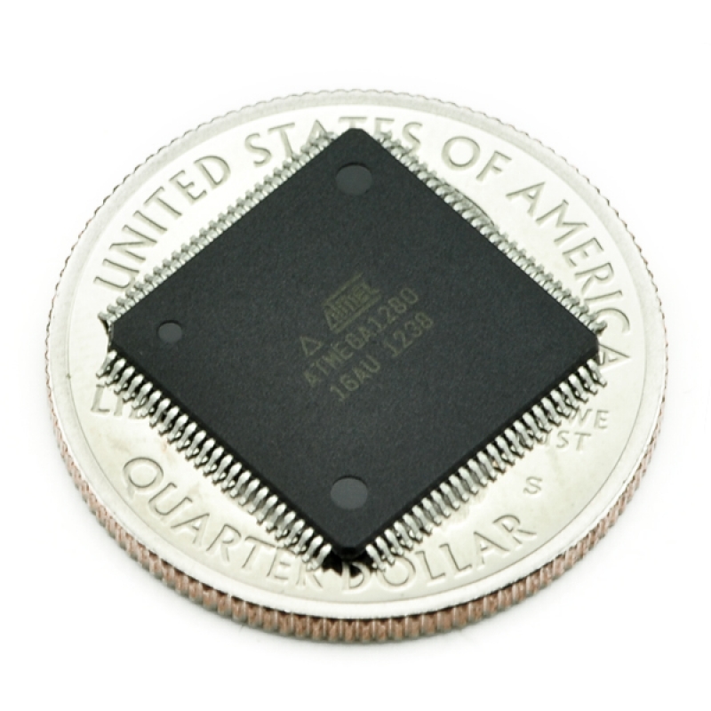
Break IC ATMEGA1280A Binary
Break IC ATmega1280A microcontroller tamper resistance system and recover atmega1280a microprocessor fuse bit, readout embedded firmware file from flash memory and eeprom memory;
Break IC ATmega1280A microcontroller tamper resistance system and decrypt atmega1280a microprocessor fuse bit, readout embedded firmware file from flash memory and eeprom memory
The 16-bit Timer/Counter unit allows accurate program execution timing (event management), wave generation, and signal timing measurement. The main features are:
True 16-bit Design (i.e., Allows 16-bit PWM)
Three independent Output Compare Units
Double Buffered Output Compare Registers
One Input Capture Unit
Input Capture Noise Canceler
Clear Timer on Compare Match (Auto Reload)
Glitch-free, Phase Correct Pulse Width Modulator (PWM)
Variable PWM Period
Frequency Generator
External Event Counter
Twenty independent interrupt sources (TOV1, OCF1A, OCF1B, OCF1C, ICF1, TOV3,
OCF3A, OCF3B, OCF3C, ICF3, TOV4, OCF4A, OCF4B, OCF4C, ICF4, TOV5, OCF5A, OCF5B, OCF5C and ICF5)
Most register and bit references in this section are written in general form. A lower case “n” replaces the Timer/Counter number, and a lower case “x” replaces the Output Compare unit channel. However, when using the register or bit defines in a program, the precise form must be used, i.e., TCNT1 for accessing Timer/Counter1 counter value and so on.
A simplified block diagram of the 16-bit Timer/Counter is shown in Figure 49. For the actual placement of I/O pins, see “Pinout ATmega640/1280/2560” on page 2 and “Pinout ATmega1281/2561” on page 3. CPU accessible I/O Registers, including I/O bits and I/O pins, are shown in bold when crack mcu atmega1280 eeprom and flash memory.
hack locked atmega1280a mcu flash memory after decap microcontroller atmega1280a mcu package and dump heximal code from flash memory
The device-specific I/O Register and bit locations are listed in the “16-bit Timer/Counter Register Description”.
The Power Reduction Timer/Counter1 bit, PRTIM1, in “Power Reduction Register 0 – PRR0” on page 54 must be written to zero to enable Timer/Counter1 module.
The Power Reduction Timer/Counter3 bit, PRTIM3, in “Power Reduction Register 1 – PRR1” on page 55 must be written to zero to enable Timer/Counter3 module.
The Power Reduction Timer/Counter4 bit, PRTIM4, in “Power Reduction Register 1 – PRR1” on page 55 must be written to zero to enable Timer/Counter4 module.
The Power Reduction Timer/Counter5 bit, PRTIM5, in “Power Reduction Register 1 – PRR1” on page 55 must be written to zero to enable Timer/Counter5 module.
Timer/Counter4 and Timer/Counter5 only have full functionality in the ATmega640/1280/2560.
The Timer/Counter (TCNTn), Output Compare Registers (OCRnA/B/C), and Input Capture Register (ICRn) are all 16-bit registers.
Special procedures must be followed when accessing the 16-bit registers. These procedures are described in the section “Accessing 16-bit Registers” on page 137. The Timer/Counter Control Registers (TCCRnA/B/C) are 8-bit registers and have no CPU access restrictions.
Interrupt requests (shorten as Int.Req.) signals are all visible in the Timer Interrupt Flag Register (TIFRn). All interrupts are individually masked with the Timer Interrupt Mask Register (TIMSKn). TIFRn and TIMSKn are not shown in the figure since these registers are shared by other timer units.
The Timer/Counter can be clocked internally, via the prescaler, or by an external clock source on the Tn pin. The Clock Select logic block controls which clock source to readout locked mcu atmega1280v flash program and edge the Timer/Counter uses to increment (or decrement) its value. The Timer/Counter is inactive when no clock source is selected. The output from the clock select logic is referred to as the timer clock (clkTn).
The double buffered Output Compare Registers (OCRnA/B/C) are compared with the Timer/Counter value at all time. The result of the compare can be used by the Waveform Generator to generate a PWM or variable frequency output on the Output Compare pin (OCnA/B/C). See “Output Compare Units” on page 144.. The compare match event will also set the Compare Match Flag (OCFnA/B/C) which can be used to generate an Output Compare interrupt request.
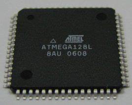
Recover Chip ATmega128PV Flash
We can Recover CHIP ATMEGA128PV Flash, please view the CHIP ATMEGA128PV features for your reference:
The simplest mode of operation is the Normal mode (WGMn3:0 = 0). In this mode the counting direction is always up (incrementing), and no counter clear is performed.
The counter simply overruns when it passes its maximum 16-bit value (MAX = 0xFFFF) and then restarts from the BOTTOM (0x0000).
In normal operation the Timer/Counter Over-flow Flag (TOVn) will be set in the same timer clock cycle as the TCNTn becomes zero.
The TOVn Flag in this case behaves like a 17th bit, except that it is only set, not cleared. However, combined with the timer overflow interrupt that automatically clears the TOVn Flag, the timer resolution can be increased by software.
There are no special cases to consider in the Normal mode, a new counter value can be written anytime. The Input Capture unit is easy to use in Normal mode. However, observe that the maximum interval between the external events must not exceed the resolution of the counter.
Recover Chip ATmega128PV Flash
If the interval between events are too long, the timer overflow interrupt or the prescaler must be used to extend the resolution for the capture unit. The Output Compare units can be used to generate interrupts at some given time.
Using the Output Compare to generate waveforms in Normal mode is not recommended, since this will occupy too much of the CPU time. In Clear Timer on Compare or CTC mode (WGMn3:0 = 4 or 12), the OCRnA or ICRn Register are used to manipulate the counter resolution.
In CTC mode the counter is cleared to zero when the counter value (TCNTn) matches either the OCRnA (WGMn3:0 = 4) or the ICRn (WGMn3:0 = 12). The OCRnA or ICRn define the top value for the counter, hence also its resolution.
This mode allows greater control of the compare match output frequency. It also simplifies the operation of counting external events. The timing diagram for the CTC mode is shown in Figure 54. The counter value (TCNTn) increases until a compare match occurs with either OCRnA or ICRn, and then counter (TCNTn) is cleared.
An interrupt can be generated at each time the counter value reaches the TOP value by either using the OCFnA or ICFn Flag according to the register used to define the TOP value. If the interrupt is enabled, the interrupt handler routine can be used for updating the TOP value. However, changing the TOP to a value close to BOTTOM when the counter is running with none or a low prescaler value must be done with care since the CTC mode does not have the double buffering feature.
If the new value written to OCRnA or ICRn is lower than the current value of TCNTn, the counter will miss the compare match. The counter will then have to count to its maximum value (0xFFFF) and wrap around starting at 0x0000 before the compare match can occur. In many cases this feature is not desirable. An alternative will then be to use the fast PWM mode using OCRnA for defining TOP (WGMn3:0 = 15) since the OCRnA then will be double buffered.
For generating a waveform output in CTC mode, the OCnA output can be set to toggle its logical level on each compare match by setting the Compare Output mode bits to toggle mode (COMnA1:0 = 1). The OCnA value will not be visible on the port pin unless the data direction for the pin is set to output (DDR_OCnA = 1).
The waveform generated will have a maximum frequency of fOCnA = fclk_I/O/2 when OCRnA is set to zero (0x0000). The waveform frequency is defined by the following equation.
Reverse Engineering PLD GAL16V8 Software
We can Reverse Engineering PLD GAL16V8 Software after break gal16v8 pld memory fuse bit and readout its jed file;
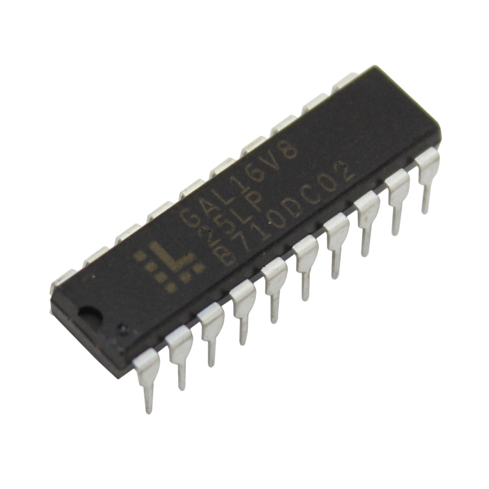
crack pld gal16v8 fuse bit and dump its embedded pof or jed file from memory
The Output Compare Register B contains an 8-bit value that is continuously compared with the counter value (TCNT0). A match can be used to generate an Output Compare interrupt, or to generate a waveform output on the OC0B pin.
Bit 2 – OCF0B: Timer/Counter 0 Output Compare B Match Flag
The OCF0B bit is set when a Compare Match occurs between the Timer/Counter and the data in OCR0B – Output Compare Register0 B. OCF0B is cleared by hardware when executing the corresponding interrupt handling vector.
Alternatively, OCF0B is cleared by writing a logic one to the flag. When the I-bit in SREG, OCIE0B (Timer/Counter Compare B Match Interrupt Enable), and OCF0B are set, the Timer/Counter Compare Match Interrupt is executed.
Bit 1 – OCF0A: Timer/Counter 0 Output Compare A Match Flag
Reverse Engineering PLD GAL16V8 Software
The OCF0A bit is set when a Compare Match occurs between the Timer/Counter0 and the data in OCR0A – Output Compare Register0. OCF0A is cleared by hardware when executing the corresponding interrupt handling vector.
Alternatively, OCF0A is cleared by writing a logic one to the flag. When the I-bit in SREG, OCIE0A (Timer/Counter0 Compare Match Interrupt Enable), and OCF0A are set, the Timer/Counter0 Compare Match Interrupt is executed.
Bit 0 – TOV0: Timer/Counter0 Overflow Flag
The bit TOV0 is set when an overflow occurs in Timer/Counter0. TOV0 is cleared by hardware when executing the corresponding interrupt handling vector.
Alternatively, TOV0 is cleared by writing a logic one to the flag. When the SREG I-bit, TOIE0 (Timer/Counter0 Overflow Interrupt Enable), and TOV0 are set, the Timer/Counter0 Overflow interrupt is executed. The setting of this flag is dependent of the WGM02:0 bit setting. Refer to Table 76, “Waveform Generation Mode Bit Description” on page 130.
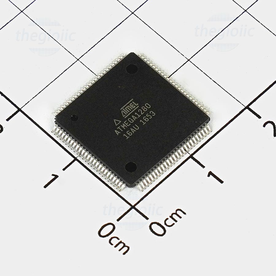
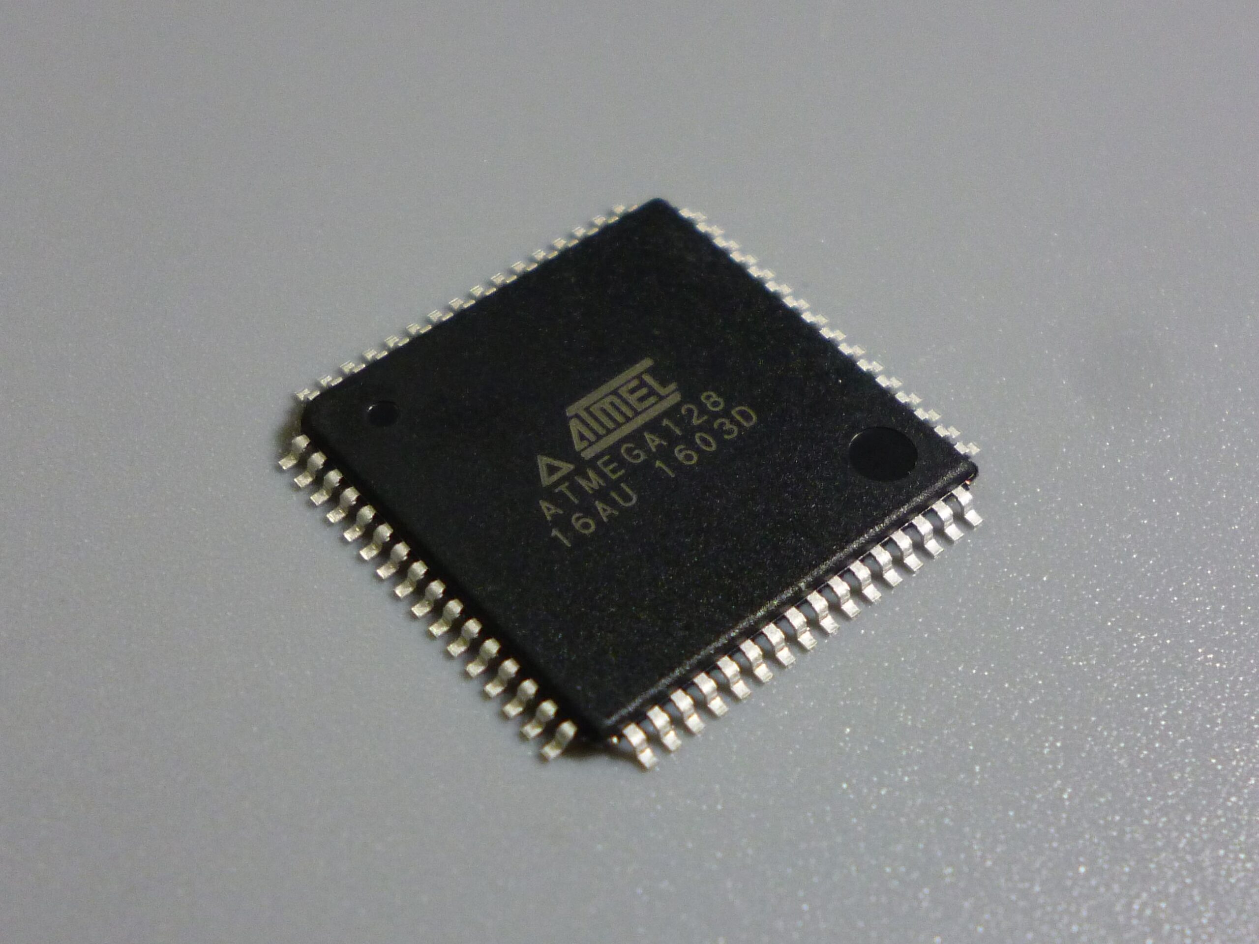
Break MCU ATmega1280PV Code
Break MCU ATmega1280PV Code can help engineer to recover embedded firmware such as heximal from flash memory and atmega128 microcontroller;
Break MCU ATmega1280PV Code can help engineer to recover embedded firmware such as heximal from flash memory and atmega128 microcontroller;
The FOC0A bit is only active when the WGM bits specify a non-PWM mode. However, for ensuring compatibility with future devices, this bit must be set to zero when TCCR0B is written when operating in PWM mode.
When writing a logical one to the FOC0A bit, an immediate Compare Match is forced on the Waveform Generation unit.
The OC0A output is changed according to its COM0A1:0 bits setting. Note that the FOC0A bit is implemented as a strobe. Therefore it is the value present in the COM0A1:0 bits that determines the effect of the forced compare. A FOC0A strobe will not generate any interrupt, nor will it clear the timer in CTC mode using OCR0A as TOP in the process of breaking off atmega128 microcontroller protection. The FOC0A bit is always read as zero. The FOC0B bit is only active when the WGM bits specify a non-PWM mode.
However, for ensuring compatibility with future devices, this bit must be set to zero when TCCR0B is written when operating in PWM mode. When writing a logical one to the FOC0B bit, an immediate Compare Match is forced on the Waveform Generation unit.The OC0B output is changed according to its COM0B1:0 bits setting. Note that the FOC0B bit is implemented as a strobe.
Therefore it is the value present in the COM0B1:0 bits that determines the effect of the forced compare. A FOC0B strobe will not generate any interrupt, nor will it clear the timer in CTC mode using OCR0B as TOP. The FOC0B bit is always read as zero. The Timer/Counter Register gives direct access, both for read and write operations, to the Timer/Counter unit 8-bit counter. Writing to the TCNT0 Register blocks (removes) the Compare Match on the following timer clock.
Modifying the counter (TCNT0) while the counter is running, introduces a risk of missing a Compare Match between TCNT0 and the OCR0x Registers. The Output Compare Register A contains an 8-bit value that is continuously compared with the counter value (TCNT0). A match can be used to generate an Output Compare interrupt, or to generate a waveform output on the OC0A pin.
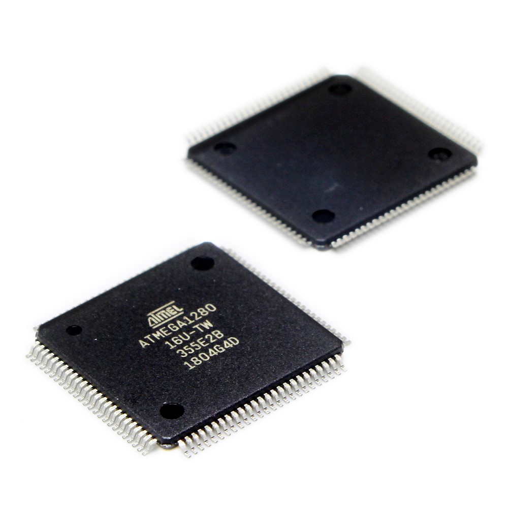
Recover MCU ATmega1280P Eeprom
Recover MCU ATmega1280P Eeprom content as well as flash program in the format of binary or heximal and copy the firmware to new microcontroller atmega1280p;
Recover MCU ATmega1280P Eeprom content as well as flash program in the format of binary or heximal and copy the firmware to new microcontroller atmega1280p;
The N variable represents the prescale factor (1, 8, 64, 256, or 1024). The extreme values for the OCR0A Register represent special cases when generating a PWM waveform output in the phase correct PWM mode. If the OCR0A is set equal to BOTTOM, the output will be continuously low and if set equal to MAX the output will be continuously high for non-inverted PWM mode. For inverted PWM the output will have the opposite logic values.
crack atmega1280p microprocessor fuse bit and readout embedded firmware from flash memory and eeprom memory
At the very start of period 2 in Figure 44 OCnx has a transition from high to low even though there is no Compare Match. The point of this transition is to guarantee symmetry around BOTTOM. There are two cases that give a transition without Compare Match. OCR0A changes its value from MAX, like in Figure 44. When the OCR0A value is MAX the OCn pin value is the same as the result of a down-counting Compare Match.
To ensure symmetry around BOTTOM the OCn value at MAX must correspond to the result of an up-counting Compare Match. The timer starts counting from a value higher than the one in OCR0A, and for that reason misses the Compare Match and hence the OCn change that would have happened on the way up. The Timer/Counter is a synchronous design and the timer clock (clkT0) is therefore shown as a clock enable signal in the following figures. The figures include information on when Interrupt Flags are set. Figure 45 contains timing data for basic Timer/Counter operation.
The figure shows the count sequence close to the MAX value in all modes other than phase correct PWM mode. These bits control the Output Compare pin (OC0B) behavior to recover atmega1280 mcu embedded heximal file. If one or both of the COM0B1:0 bits are set, the OC0B output overrides the normal port functionality of the I/O pin it is connected.
However, note that the Data Direction Register (DDR) bit corresponding to the OC0B pin must be set in order to enable the output driver. When OC0B is connected to the pin, the function of the COM0B1:0 bits depends on the WGM02:0 bit setting. Table 70 shows the COM0A1:0 bit functionality when the WGM02:0 bits are set to a normal or CTC mode (non-PWM).
Combined with the WGM02 bit found in the TCCR0B Register, these bits control the counting sequence of the counter, the source for maximum (TOP) counter value, and what type of waveform generation to be used. Modes of operation supported by the Timer/Counter unit are: Normal mode (counter), Clear Timer on Compare Match (CTC) mode, and two types of Pulse Width Modulation (PWM) modes.