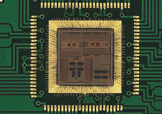
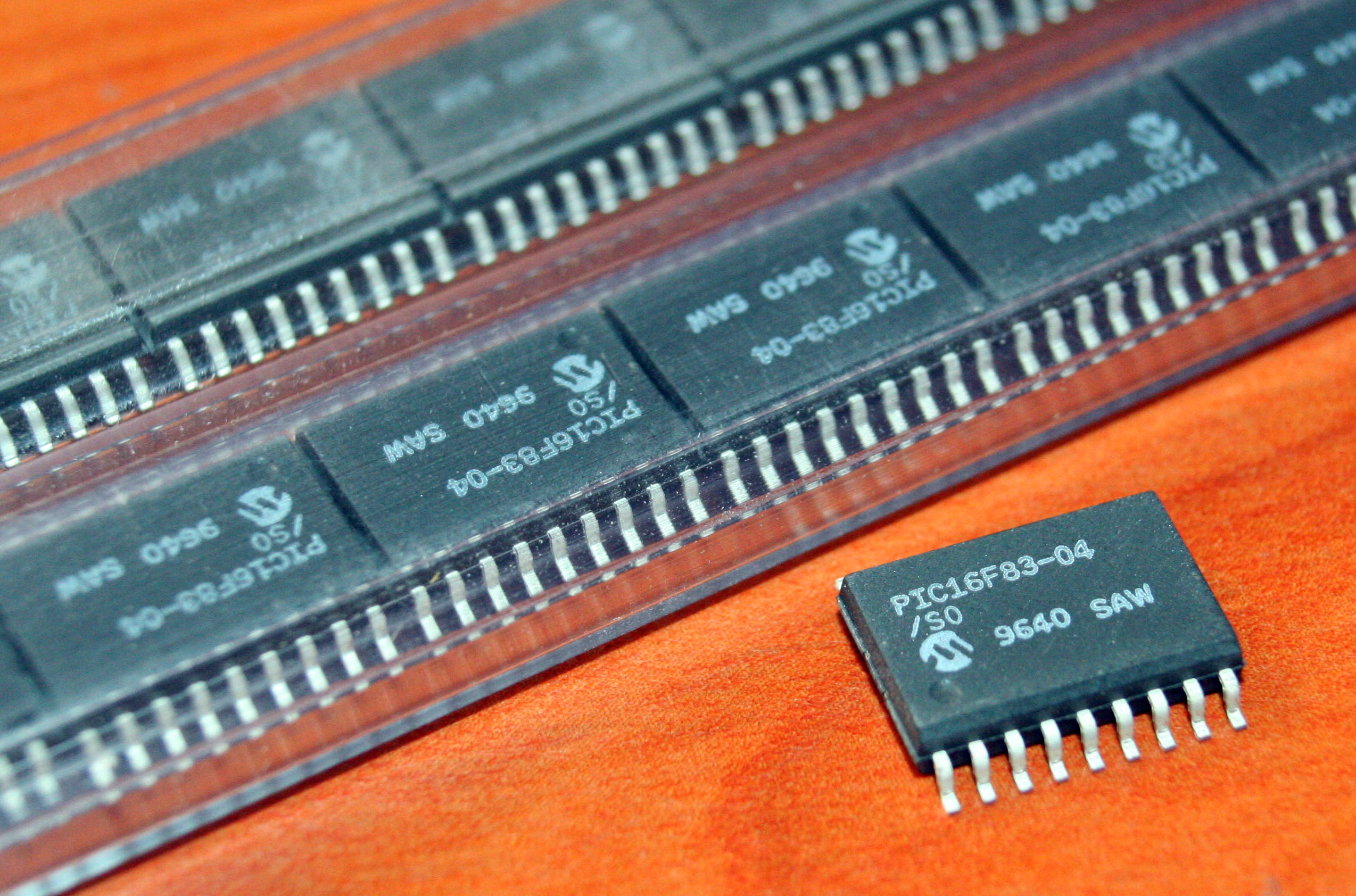
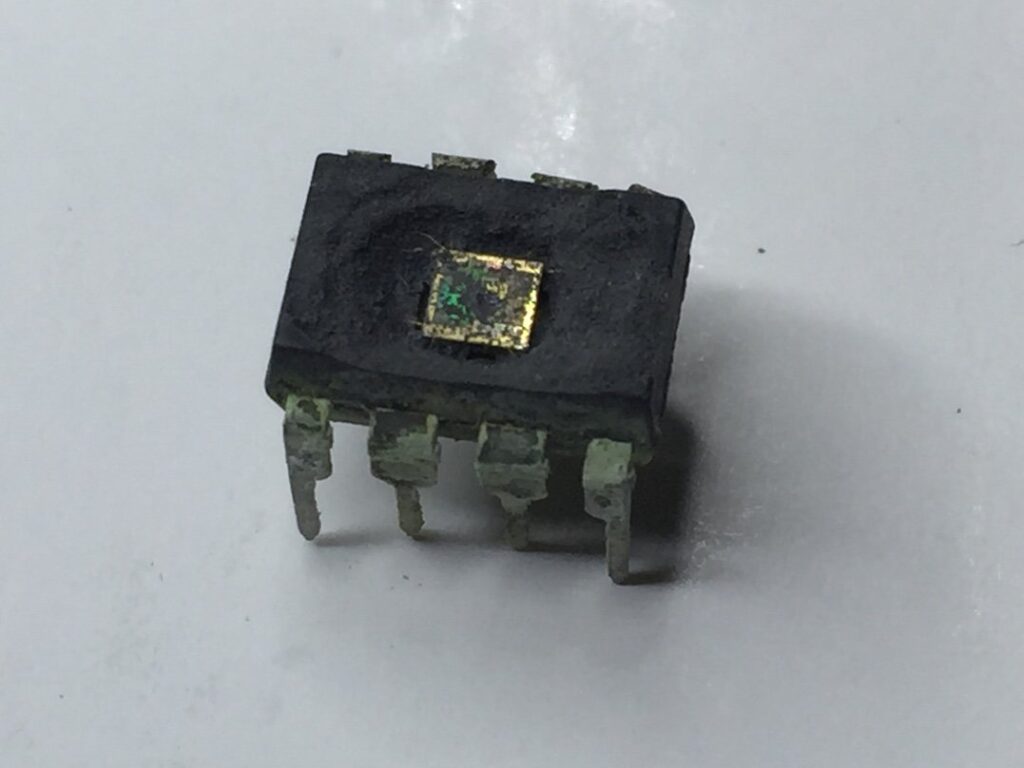
 Break MCU PIC16F628A Program
Break MCU PIC16F628A Program is a process to attack microchip microcontroller pic16f628a security fuse bit by focus ion beam and then copy embedded heximal from pic16f628a flash memory;
ICFn is automatically cleared when the Input Capture Interrupt Vector is executed. Alternatively, ICFn can be cleared by writing a logic one to its bit location.
Bit 3– OCFnC: Timer/Countern, Output Compare C Match Flag
This flag is set in the timer clock cycle after the counter (TCNTn) value matches the Output Compare Register C (OCRnC).
Note that a Forced Output Compare (FOCnC) strobe will not set the OCFnC Flag. OCFnC is automatically cleared when the Output Compare Match C Interrupt Vector is executed. Alternatively, OCFnC can be cleared by writing a logic one to its bit location.
Bit 2 – OCFnB: Timer/Counter1, Output Compare B Match Flag
This flag is set in the timer clock cycle after the counter (TCNTn) value matches the Output Compare Register B (OCRnB).
Note that a Forced Output Compare (FOCnB) strobe will not set the OCFnB Flag. OCFnB is automatically cleared when the Output Compare Match B Interrupt Vector is executed. Alternatively, OCFnB can be cleared by writing a logic one to its bit location if Break microcontroller pic16f628a memory.
Bit 1 – OCF1A: Timer/Counter1, Output Compare A Match Flag
This flag is set in the timer clock cycle after the counter (TCNTn value matches the Output Compare Register A (OCRnA).
Note that a Forced Output Compare (FOCnA) strobe will not set the OCFnA Flag. OCFnA is automatically cleared when the Output Compare Match A Interrupt Vector is executed. Alternatively, OCFnA can be cleared by writing a logic one to its bit location.
Bit 0 – TOVn: Timer/Countern, Overflow Flag
The setting of this flag is dependent of the WGMn3:0 bits setting. In Normal and CTC modes, the TOVn Flag is set when the timer overflows. Refer to Table 82 on page 160 for the TOVn Flag behavior when using another WGMn3:0 bit setting if attacking pic16f711 MCU memory.
TOVn is automatically cleared when the Timer/Countern Overflow Interrupt Vector is executed. Alternatively, TOVn can be cleared by writing a logic one to its bit location.
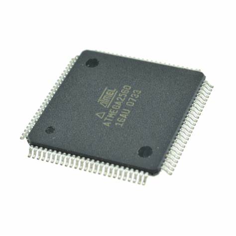
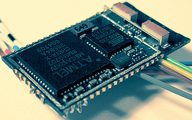
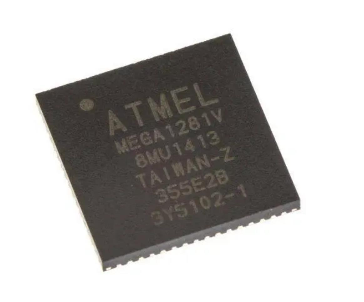
Reverse Engineering Chip ATmega2560P Code
Reverse Engineering Chip ATmega2560P and copy microcontroller atmega2560p source Code from its flash and eeprom memory, rewrite firmware heximal to new processor atmega2560p to make MCU cloning units;
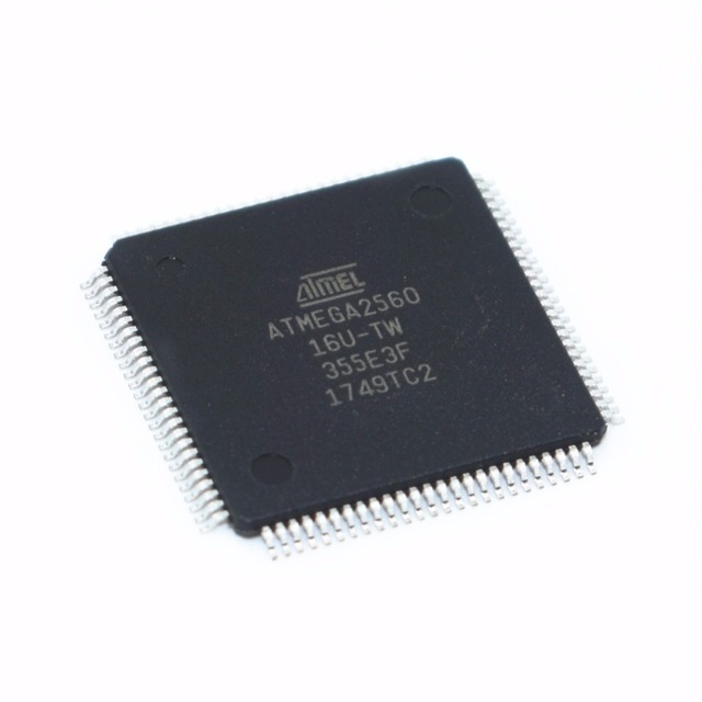
Reverse Engineering Chip ATmega2560P and copy microcontroller atmega2560p source Code from its flash and eeprom memory, rewrite firmware heximal to new processor atmega2560p to make MCU cloning units;
When this bit is written to one, and the I-flag in the Status Register is set (interrupts globally enabled), the Timer/Countern Input Capture interrupt is enabled. The corresponding Interrupt Vector (See “Interrupts” on page 69.) is executed when the ICFn Flag, located in TIFRn, is set.
Bit 3 – OCIEnC: Timer/Countern, Output Compare C Match Interrupt Enable
When this bit is written to one, and the I-flag in the Status Register is set (interrupts globally enabled), the Timer/Countern Output Compare C Match interrupt is enabled. The corresponding Interrupt Vector (See “Interrupts” on page 69.) is executed when the OCFnC Flag, located in TIFRn, is set.
Bit 2 – OCIEnB: Timer/Countern, Output Compare B Match Interrupt Enable
When this bit is written to one, and the I-flag in the Status Register is set (interrupts globally enabled), the Timer/Countern Output Compare B Match interrupt is enabled. The corresponding Interrupt Vector (See “Interrupts” on page 69.) is executed when the OCFnB Flag, located in TIFRn, is set before copy microcontroller pic16c771 firmware.
Bit 1 – OCIEnA: Timer/Countern, Output Compare A Match Interrupt Enable
When this bit is written to one, and the I-flag in the Status Register is set (interrupts globally enabled), the Timer/Countern Output Compare A Match interrupt is enabled. The corresponding Interrupt Vector (See “Interrupts” on page 69.) is executed when the OCFnA Flag, located in TIFRn, is set.
unlock atmega2560p atmel microcomputer protection and copy atmega2560p mcu chip memory content
Bit 0 – TOIEn: Timer/Countern, Overflow Interrupt Enable
When this bit is written to one, and the I-flag in the Status Register is set (interrupts globally enabled), the Timer/Countern Overflow interrupt is enabled. The corresponding Interrupt Vector (See “Interrupts” on page 69.) is executed when the TOVn Flag, located in TIFRn, is set.
Bit 5 – ICFn: Timer/Countern, Input Capture Flag
This flag is set when a capture event occurs on the ICPn pin. When the Input Capture Register (ICRn) is set by the WGMn3:0 to be used as the TOP value, the ICFn Flag is set when the counter reaches the TOP value.
Recover Chip PIC16F83 Eeprom
Recover Chip PIC16F83 Eeprom content by cracking locked microcontroller pic16f83 security fuse bit and then extract embedded code from microchip MCU;
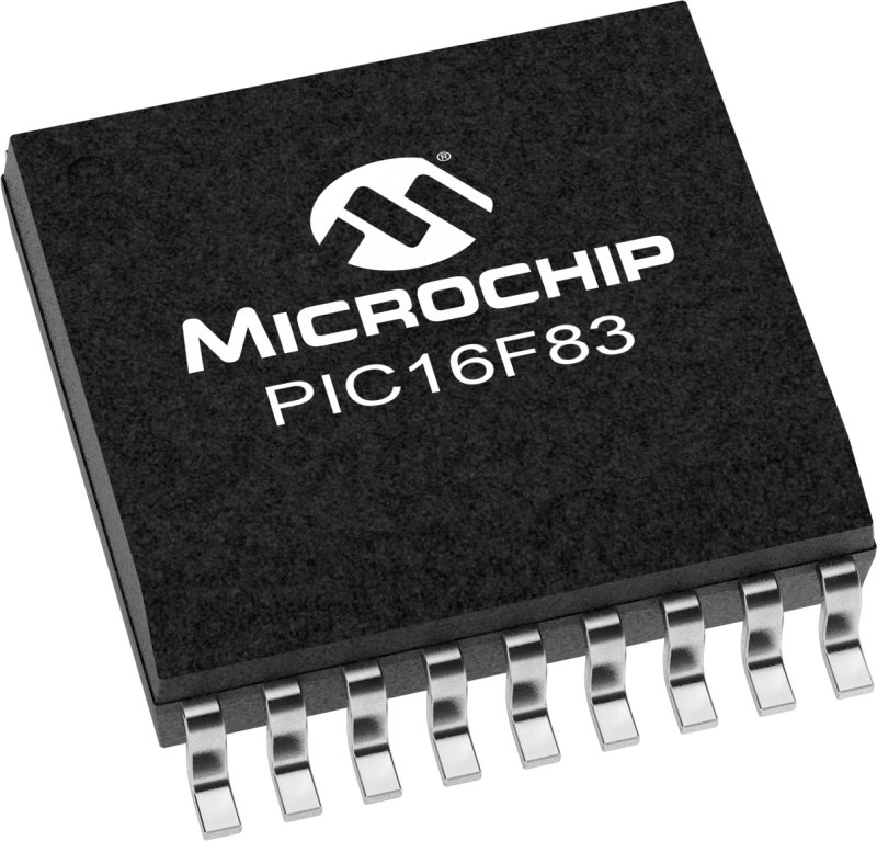
Recover Chip PIC16F83 Eeprom content by cracking locked microcontroller pic16f83 security fuse bit and then extract embedded code from microchip MCU
We can Recover Chip PIC16F83 Eeprom, please view the Chip PIC16F83 features for your reference:
High Performance RISC CPU Features:
• Only 35 single word instructions to learn
• All instructions single cycle except for program branches which are two-cycle Operating speed: DC – 10 MHz clock input
DC – 400 ns instruction cycle
14-bit wide instructions
8-bit wide data path
15 special function hardware registers
Eight-level deep hardware stack
Direct, indirect and relative addressing modes
Four interrupt sources:
– External RB0/INT pin
– TMR0 timer overflow
– PORTB<7:4> interrupt on change
– Data EEPROM write complete
· 1000 erase/write cycles Flash program memory
· 10,000,000 erase/write cycles EEPROM data memory
· EEPROM Data Retention > 40 years
Peripheral Features:
· 13 I/O pins with individual direction control
· High current sink/source for direct LED drive
– 25 mA sink max. per pin before Recover Chip
– 20 mA source max. per pin
· TMR0: 8-bit timer/counter with 8-bit programmable prescaler
Special Microcontroller Features:
· In-Circuit Serial Programming (ICSP™) – via two pins (ROM devices support only Data EEPROM programming)
· Power-on Reset (POR)
crack pic16f83 microchip processor and copy mcu pic16f83 memory file
· Power-up Timer (PWRT)
· Oscillator Start-up Timer (OST)
· Watchdog Timer (WDT) with its own on-chip RC oscillator for reliable operation
· Code-protection
· Power saving SLEEP mode
· Selectable oscillator options
CMOS Flash/EEPROM Technology:
Low-power, high-speed technology
· Fully static design
· Wide operating voltage range:
– Commercial: 2.0V to 6.0V
– Industrial: 2.0V to 6.0V
· Low power consumption:
– < 2 mA typical @ 5V, 4 MHz
– 15 µA typical @ 2V, 32 kHz
– < 1 µA typical standby current @ 2V
Circuit Engineering Company Limited continues to be recognized as the Southern China Leader in Services for IC Read, MCU Recover, Chip Extract, Microcontroller Unlock service.
With the advancement of today’s modern circuit board technology, it is more important than ever to have specialists available to help you at a moment’s notice. Our engineering and commercial teams collectively have a vast amount of electronic experience covering field include Consumer Electronics, Industrial Automation Electronics, Wireless Communication Electronics., etc. For more information please contact us through email.
Break MCU
As for MCU break (microcontroller unit), hardware security in microcontrollers is being constantly improved. Because the tools for mcu break are becoming more sophisticated, better and better security protection is required. Rapid co-evolution is driven by this continuous battle between chip manufacturers and chip attackers.
Another threat that must be considered is that a great deal of second-hand semiconductor manufacturing and testing equipment appears on the market. It cannot be used to break high-end MCUs, but should be enough to break MCU chips manufactured with older technology. For example, while 90 nm manufacturing technology is currently leading-edge, most MCUs are produced with 0.35 µm technology and smartcards with 0.25 µm technology.
Circuit Engineering Company Limited continues to be recognized as the Southern China Leader in Services for read IC, MCU break, Chip decrypt, Microcontroller copy service. With the advancement of today’s modern circuit board technology, it is more important than ever to have specialists available to help you at a moment’s notice. Our engineering and commercial teams collectively have a vast amount of electronic experience covering field include Consumer Electronics, Industrial Automation Electronics, Wireless Communication Electronics., etc. For more information please contact us through email.
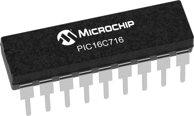
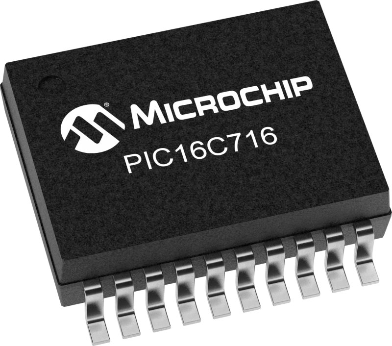
Reverse Engineering Microcontroller PIC16C716 Heximal
Reverse engineering Microcontroller PIC16C716 can locate the security fuse bit of it, and break off it in order to take the embedded software from mcu pic16c716, and then copy the microprocessor pic16c716 program out to new MCU;

Reverse engineering Microcontroller PIC16C716 can locate the security fuse bit of it, and break off it in order to take the embedded software from mcu pic16c716, and then copy the microprocessor pic16c716 program out to new MCU
There are two memory blocks in each of these PICmicro® microcontroller devices. Each block (Program Memory and Data Memory) has its own bus so that concurrent access can occur.
Additional information on device memory may be found in the PICmicro Mid-Range Reference Manual, (DS33023).
The PIC16C712/716 has a 13-bit program counter capable of addressing an 8K x 14 program memory space. PIC16C712 has 1K x 14 words of program memory and PIC16C716 has 2K x 14 words of program memory. Accessing a location above the physically implemented address will cause a wraparound.
The reset vector is at 0000h and the interrupt vector is at 0004h.
Each bank extends up to 7Fh (128 bytes). The lower locations of each bank are reserved for the Special
Function Registers. Above the Special Function Registers are General Purpose Registers, implemented as static RAM. All implemented banks contain special function registers. Some “high use” special function registers from one bank may be mirrored in another bank for code reduction and quicker access.
The Special Function Registers are registers used by the CPU and Peripheral Modules for controlling the desired operation of the device. These registers are implemented as static RAM. A list of these registers is give in Table 2-1 after attacking Microcontroller.
The special function registers can be classified into two sets; core (CPU) and peripheral. Those registers associated with the core functions are described in detail in this section. Those related to the operation of the peripheral features are described in detail in that peripheral feature section.
cracking secured mcu PIC16C716 flash memory and readout embedded flash memory binary and heximal file
The STATUS register, shown in Figure 2-4, contains the arithmetic status of the ALU, the RESET status and the bank select bits for data memory. The STATUS register can be the destination for any instruction, as with any other register. If the STATUS register is the destination for an instruction that affects the Z, DC or C bits, then the write to these three bits is disabled. These bits are set or cleared according to the device logic. Furthermore, the TO and PD bits are not writable. Therefore, the result of an instruction with the STATUS register as destination may be different than intended.
The program counter (PC) specifies the address of the instruction to fetch for execution. The PC is 13 bits wide. The low byte is called the PCL register after Reverse engineering Microcontroller. This register is readable and writable. The high byte is called the PCH register. This register contains the PC<12:8> bits and is not directly readable or writable. All updates to the PCH register go through the PCLATH register.
The stack allows a combination of up to 8 program calls and interrupts to occur. The stack contains the return address from this branch in program execution. Midrange devices have an 8 level deep x 13-bit wide hardware stack. The stack space is not part of either program or data space and the stack pointer is not readable or writable. The PC is PUSHed onto the stack when a CALL instruction is executed or an interrupt causes a branch. The stack is POPed in the event of a RETURN, RETLW or a RETFIE instruction execution when Reverse engineering Microcontroller.
PCLATH is not modified when the stack is PUSHed or POPed. After the stack has been PUSHed eight times, the ninth push overwrites the value that was stored from the first push. The tenth push overwrites the second push (and so on). The CALL and GOTO instructions provide 11 bits of address to allow branching within any 2K program memory page. When doing a CALL or GOTO instruction, the upper bit of the address is provided by PCLATH<3>.
unlock encrypted microcontroller pic16c716 flash memory and extract embedded firmware in the format of binary or heximal
When doing a CALL or GOTO instruction, the user must ensure that the page select bit is programmed so that the desired program memory page is addressed. If a return from a CALL instruction (or interrupt) is executed, the entire 13-bit PC is pushed onto the stack. Therefore, manipulation of the PCLATH<3> bit is not required for the return instructions (which POPs the address from the stack).
For example, CLRF STATUS will clear the upper-three bits and set the Z bit. This leaves the STATUS register as 000u u1uu (where u = unchanged).
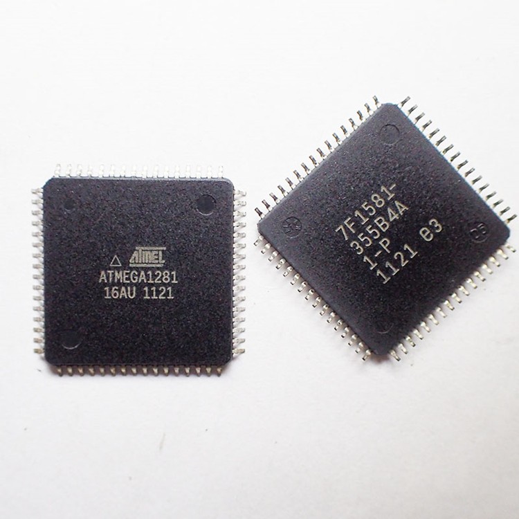
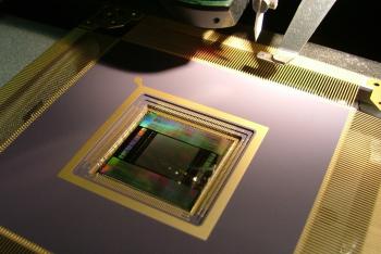
Recover Microprocessor ATmega1281PA Flash
Recover Microprocessor ATmega1281PA Flash heximal file, copy mcu atmega1281pa memory content to new microcontroller and provide the same functions, the security fuse bit of microcontroller atmega1281pa will be cracked reset the status.
The FOCnA/FOCnB/FOCnC bits are only active when the WGMn3:0 bits specifies a non-PWM mode. When writing a logical one to the FOCnA/FOCnB/FOCnC bit, an immediate compare match is forced on the waveform generation unit.
Recover Microprocessor ATmega1281PA Flash heximal file, copy mcu atmega1281pa memory content to new microcontroller and provide the same functions, the security fuse bit of microcontroller atmega1281pa will be cracked reset the status.
The OCnA/OCnB/OCnC output is changed according to its COMnx1:0 bits setting. Note that the FOCnA/FOCnB/FOCnC bits are implemented as strobes. Therefore it is the value present in the COMnx1:0 bits that determine the effect of the forced compare.
A FOCnA/FOCnB/FOCnC strobe will not generate any interrupt nor will it clear the timer in Clear Timer on Compare Match (CTC) mode using OCRnA as TOP before break microcontroller pic16f886.

unlock encrypted mcu atmega1281 microcontroller fuse bit and dump embedded firmware from flash memory and eeprom memory
The two Timer/Counter I/O locations (TCNTnH and TCNTnL, combined TCNTn) give direct access, both for read and for write operations, to the Timer/Counter unit 16-bit counter after Recover MICROPROCESSOR flash.
To ensure that both the high and low bytes are read and written simultaneously when the CPU accesses these registers, the access is performed using an 8-bit temporary High Byte Register (TEMP). This temporary register is shared by all the other 16-bit registers. See “Accessing 16-bit Registers” on page 137.
Modifying the counter (TCNTn) while the counter is running introduces a risk of missing a compare match between TCNTn and one of the OCRnx Registers when attacking dsp mcu texas instrument tms320f2401pg hex.
Writing to the TCNTn Register blocks (removes) the compare match on the following timer clock for all compare units. The Output Compare Registers contain a 16-bit value that is continuously compared with the counter value (TCNTn).
A match can be used to generate an Output Compare interrupt, or to generate a waveform output on the OCnx pin. The Output Compare Registers are 16-bit in size. To ensure that both the high and low bytes are written simultaneously when the CPU writes to these registers, the access is performed using an 8-bit temporary High Byte Register (TEMP).
recover secured microprocessor ATMEGA1281 flash memory and readout mcu embedded firmware from flash program memory and eeprom data memory
This temporary register is shared by all the other 16-bit registers. See “Accessing 16-bit Registers” on page 137. The Input Capture is updated with the counter (TCNTn) value each time an event occurs on the ICPn pin (or optionally on the Analog Comparator output for Timer/Counter1).
The Input Capture can be used for defining the counter TOP value. The Input Capture Register is 16-bit in size. To ensure that both the high and low bytes are read simultaneously when the CPU accesses these registers, the access is performed using an 8-bit temporary High Byte Register (TEMP).
This temporary register is shared by all the other 16-bit registers. See “Accessing 16-bit Registers” on page 137.
Break IC ATmega1281A Flash
Break IC ATmega1281A and copy microcontroller atmega128a Flash content in the format of heximal, the fuse bit of mcu atmega1281a will be unlocked by focus ion beam technique;
The Timer/Counter is a synchronous design and the timer clock (clkTn) is therefore shown as a clock enable signal in the following figures.
The figures include information on when Interrupt Flags are set, and when the OCRnx Register is updated with the OCRnx buffer value (only for modes utilizing double buffering). Figure 58 shows a timing diagram for the setting of OCFnx.
The COMnA1:0, COMnB1:0, and COMnC1:0 control the output compare pins (OCnA, OCnB, and OCnC respectively) behavior. If one or both of the COMnA1:0 bits are written to one, the OCnA output overrides the normal port functionality of the I/O pin it is connected to when recover chip atmega1281pv flash.
If one or both of the COMnB1:0 bits are written to one, the OCnB output overrides the normal port functionality of the I/O pin it is connected to.
If one or both of the COMnC1:0 bits are written to one, the OCnC output overrides the normal port functionality of the I/O pin it is connected to. However, note that the Data Direction Register (DDR) bit corresponding to the OCnA, OCnB or OCnC pin must be set in order to enable the output driver.
When the OCnA, OCnB or OCnC is connected to the pin, the function of the COMnx1:0 bits is dependent of the WGMn3:0 bits setting. Table 79 shows the COMnx1:0 bit functionality when the WGMn3:0 bits are set to a normal or a CTC mode (non-PWM) if recover mcu atmega169pa code.
Combined with the WGMn3:2 bits found in the TCCRnB Register, these bits control the counting sequence of the counter, the source for maximum (TOP) counter value, and what type of waveform generation to be used, see Table 82.
Modes of operation supported by the Timer/Counter unit are: Normal mode (counter), Clear Timer on Compare match (CTC) mode, and three types of Pulse Width Modulation (PWM) modes. (See “Modes of Operation” on page 147.).

recover atmega1281 microcontroller embedded firmware and crack atmega1281 mcu fuse bit
Setting this bit (to one) activates the Input Capture Noise Canceler. When the Noise Canceler is activated, the input from the Input Capture Pin (ICPn) is filtered. The filter function requires four successive equal valued samples of the ICPn pin for changing its output after recover chip atmega128apv source code.
The input capture is therefore delayed by four Oscillator cycles when the noise canceler is enabled.
This bit selects which edge on the Input Capture Pin (ICPn) that is used to trigger a capture event. When the ICESn bit is written to zero, a falling (negative) edge is used as trigger, and when the ICESn bit is written to one, a rising (positive) edge will trigger the capture.
When a capture is triggered according to the ICESn setting, the counter value is copied into the Input Capture Register (ICRn). The event will also set the Input Capture Flag (ICFn), and this can be used to cause an Input Capture Interrupt, if this interrupt is enabled.
When the ICRn is used as TOP value (see description of the WGMn3:0 bits located in the TCCRnA and the TCCRnB Register), the ICPn is disconnected and consequently the input capture function is disabled.
The FOCnA/FOCnB/FOCnC bits are only active when the WGMn3:0 bits specifies a non-PWM mode. When writing a logical one to the FOCnA/FOCnB/FOCnC bit, an immediate compare match is forced on the waveform generation unit.
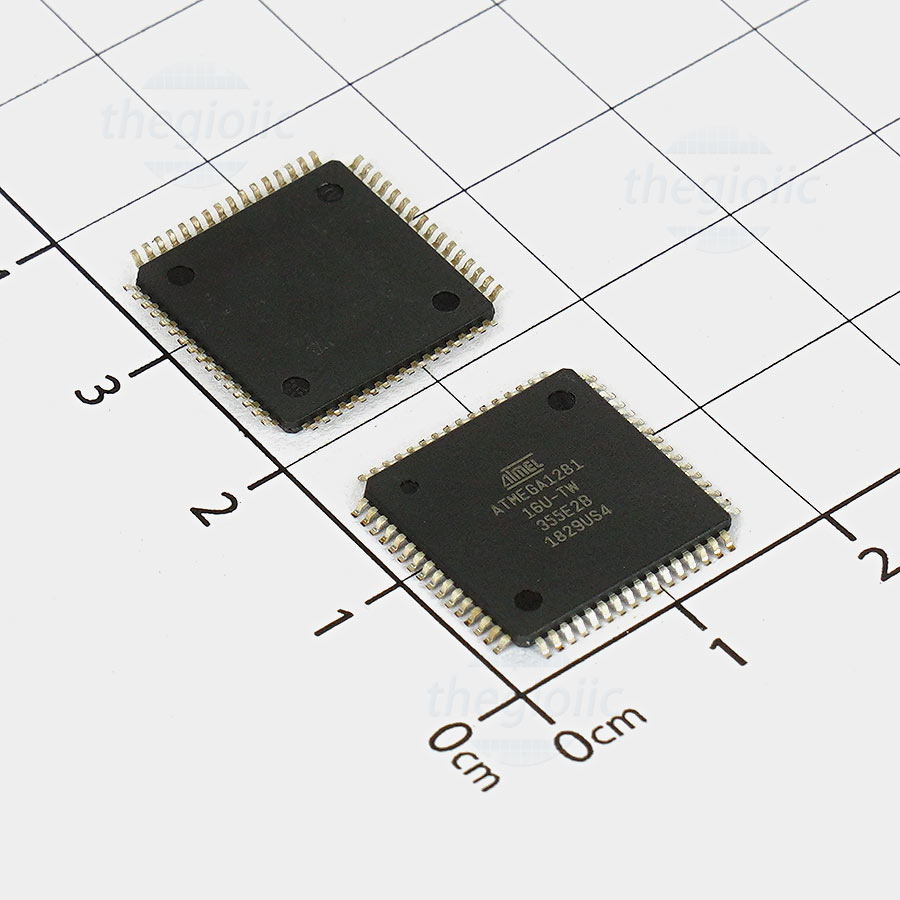
Reverse Engineering MCU ATmega1281P Firmware
Reverse Engineering MCU ATmega1281P and copy embedded Firmware from microcontroller atmega1281p memory to new MCU, to make microprocessor atmega1281p cloning units.
The Timer/Counter Overflow Flag (TOVn) is set at the same timer clock cycle as the OCRnx Registers are updated with the double buffer value (at BOTTOM).
When either OCRnA or ICRn is used for defining the TOP value, the OCnA or ICFn Flag set when TCNTn has reached TOP. The Interrupt Flags can then be used to generate an interrupt each time the counter reaches the TOP or BOTTOM value.
When changing the TOP value the program must ensure that the new TOP value is higher or equal to the value of all of the Compare Registers. If the TOP value is lower than any of the Compare Registers, a compare match will never occur between the TCNTn and the OCRnx before attack microcontroller mc68hc705p6a memory.
As Figure 57 shows the output generated is, in contrast to the phase correct mode, symmetrical in all periods. Since the OCRnx Registers are updated at BOTTOM, the length of the rising and the falling slopes will always be equal. This gives symmetrical output pulses and is therefore frequency correct.
Using the ICRn Register for defining TOP works well when using fixed TOP values. By using ICRn, the OCRnA Register is free to be used for generating a PWM output on OCnA before copying pic16lf877 MCU program.
However, if the base PWM frequency is actively changed by changing the TOP value, using the OCRnA as TOP is clearly a better choice due to its double buffer feature.
In phase and frequency correct PWM mode, the compare units allow generation of PWM waveforms on the OCnx pins. Setting the COMnx1:0 bits to two will produce a non-inverted PWM and an inverted PWM output can be generated by setting the COMnx1:0 to three.
crack locked microcontroller ATMEGA1281 memory and clone its heximal file from program flash and data eeprom
The actual OCnx value will only be visible on the port pin if the data direction for the port pin is set as output (DDR_OCnx). The PWM waveform is generated by setting (or clearing) the OCnx Register at the compare match between OCRnx and TCNTn when the counter increments, and clearing (or setting) the OCnx Register at compare match between OCRnx and TCNTn when the counter decrements.
The PWM frequency for the output when using phase and frequency correct PWM can be calculated by the following equation:
The N variable represents the prescaler divider (1, 8, 64, 256, or 1024). The extreme values for the OCRnx Register represents special cases when generating a PWM waveform output in the phase correct PWM mode.
If the OCRnx is set equal to BOTTOM the output will be continuously low and if set equal to TOP the output will be set to high for non-inverted PWM mode. For inverted PWM the output will have the opposite logic values. If OCR1A is used to define the TOP value (WGM13:0 = 9) and COM1A1:0 = 1, the OC1A output will toggle with a 50% duty cycle.
Recover Chip ATmega1281PV Source code
Recover Chip ATmega1281PV Source code from locked flash memory, copy embedded binary of mcu atmega1281pv to new MCU after crack mcu atmega1281pv fuse bit;
The phase and frequency correct Pulse Width Modulation, or phase and frequency correct PWM mode (WGMn3:0 = 8 or 9) provides a high resolution phase and frequency correct PWM waveform generation option.
The phase and frequency correct PWM mode is, like the phase correct PWM mode, based on a dual-slope operation. The counter counts repeatedly from BOTTOM (0x0000) to TOP and then from TOP to BOTTOM. In non-inverting Compare Output mode, the Output Compare (OCnx) is cleared on the compare match between TCNTn and OCRnx while upcounting, and set on the compare match while downcounting. In inverting Compare Output mode, the operation is inverted if Recover mcu pic16f873 hex.
The dual-slope operation gives a lower maximum operation frequency compared to the single-slope operation. However, due to the symmetric feature of the dualslope PWM modes, these modes are preferred for motor control applications.
hack ATMEGA1281 locked microprocessor fuse bit and copy heximal or binary file from flash program memory or eeprom memory data
The main difference between the phase correct, and the phase and frequency correct PWM mode is the time the OCRnx Register is updated by the OCRnx Buffer Register.
The PWM resolution for the phase and frequency correct PWM mode can be defined by either ICRn or OCRnA. The minimum resolution allowed is 2-bit (ICRn or OCRnA set to 0x0003), and the maximum resolution is 16-bit (ICRn or OCRnA set to MAX) after Recover tms320f2812pgfa microcontroller firmware.
The PWM resolution in bits can be calculated using the following equation: In phase and frequency correct PWM mode the counter is incremented until the counter value matches either the value in ICRn (WGMn3:0 = 8), or the value in OCRnA (WGMn3:0 = 9).
The counter has then reached the TOP and changes the count direction. The TCNTn value will be equal to TOP for one timer clock cycle. The timing diagram for the phase correct and frequency correct PWM mode is shown on Figure 57 if break microcontroller pic16f767 firmware.
The figure shows phase and frequency correct PWM mode when OCRnA or ICRn is used to define TOP. The TCNTn value is in the timing diagram shown as a histogram for illustrating the dual-slope operation. The diagram includes non-inverted and inverted PWM outputs.
The small horizontal line marks on the TCNTn slopes represent compare matches between OCRnx and TCNTn. The OCnx Interrupt Flag will be set when a compare match occurs.
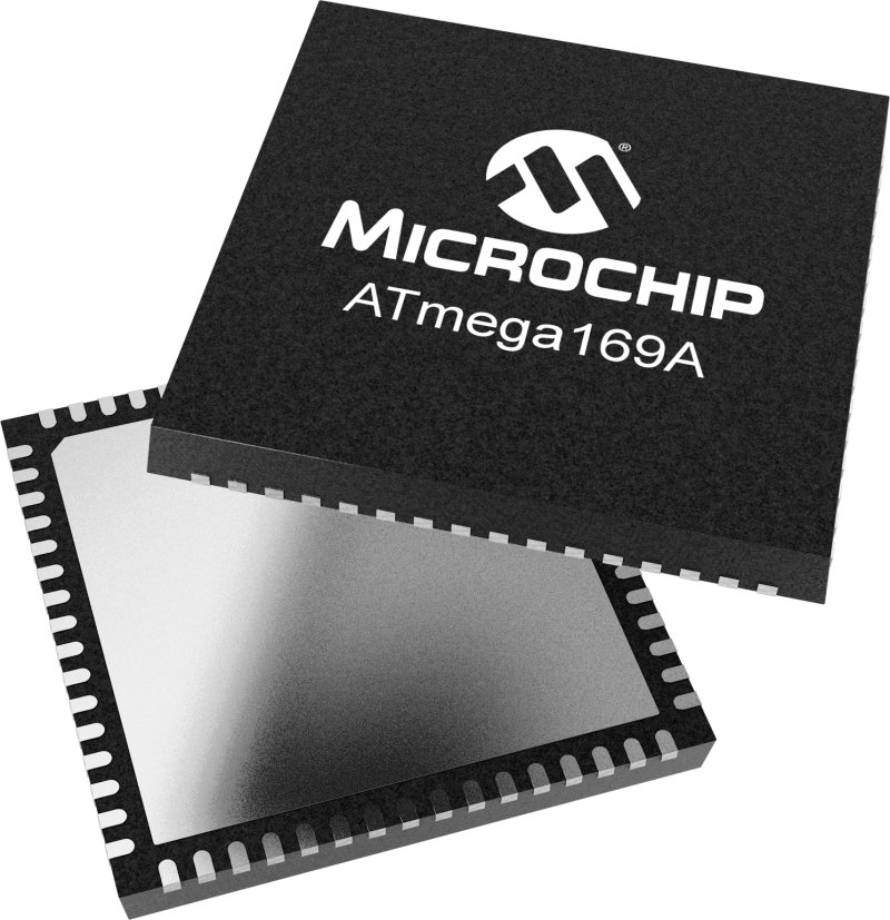
Reverse Engineering Microcontroller ATmega169A Binary
Reverse Engineering Microcontroller ATmega169A and copy mcu atmega169a Binary from its flash and eeprom memory, the tamper resistance system of microcontroller atmega169a will be unlocked;
When changing the TOP value the program must ensure that the new TOP value is higher or equal to the value of all of the Compare Registers.
If the TOP value is lower than any of the Compare Registers, a compare match will never occur between the TCNTn and the OCRnx. Note that when using fixed TOP values, the unused bits are masked to zero when any of the OCRnx Registers are written if attack pic18f66k90 MICROCONTROLLER memory.
As the third period shown in Figure 56 illustrates, changing the TOP actively while the Timer/Counter is running in the phase correct mode can result in an unsymmetrical output. The reason for this can be found in the time of update of the OCRnx Register.
Since the OCRnx update occurs at TOP, the PWM period starts and ends at TOP. This implies that the length of the falling slope is determined by the previous TOP value, while the length of the rising slope is determined by the new TOP value.
When these two values differ the two slopes of the period will differ in length. The difference in length gives the unsymmetrical result on the output.
crack ATmega169a microcomputer fuse bit and readout firmware program from flash of ATmega169a microcontroller
It is recommended to use the phase and frequency correct mode instead of the phase correct mode when changing the TOP value while the Timer/Counter is running. When using a static TOP value there are practically no differences between the two modes of operation when recover mc9s08dz32 MICROCONTROLLER embedded firmware.
In phase correct PWM mode, the compare units allow generation of PWM waveforms on the OCnx pins. Setting the COMnx1:0 bits to two will produce a non-inverted PWM and an inverted PWM output can be generated by setting the COMnx1:0 to three.
The actual OCnx value will only be visible on the port pin if the data direction for the port pin is set as output (DDR_OCnx). The PWM waveform is generated by setting (or clearing) the OCnx Register at the compare match between OCRnx and TCNTn when the counter increments, and clearing (or setting) the OCnx Register at compare match between OCRnx and TCNTn when the counter decrements.
The PWM frequency for the output when using phase correct PWM can be calculated by the following equation:
The N variable represents the prescaler divider (1, 8, 64, 256, or 1024). The extreme values for the OCRnx Register represent special cases when generating a PWM waveform output in the phase correct PWM mode.
unlock atmega169a microprocessor fuse bit and extract source code from flash memory of atmega169a mcu
If the OCRnx is set equal to BOTTOM the output will be continuously low and if set equal to TOP the output will be continuously high for non-inverted PWM mode.
For inverted PWM the output will have the opposite logic values. If OCR1A is used to define the TOP value (WGM13:0 = 11) and COM1A1:0 = 1, the OC1A output will toggle with a 50% duty cycle.