 Recovery Mcu PIC16F871 Software
Recovery Mcu PIC16F871 Software
We can Recovery Mcu PIC16F871 Software, please view the Mcu PIC16F871 features for your reference:
This document contains device-specific information.
Additional information may be found in the PICmicro™ Mid-Range Reference Manual, (DS33023), which may be obtained from your local Micromcu Sales Representative or downloaded from the Micromcu website. The Reference Manual should be considered a complementary document to this data sheet when Recovery Mcu, and is highly recommended reading for a better understanding of the device architecture and operation of the peripheral modules.
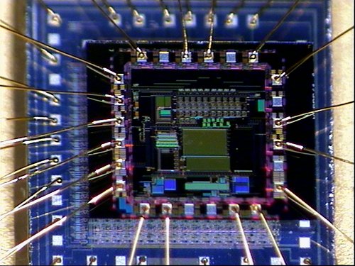
There are two devices (PIC16F870 and PIC16F871) covered by this data sheet. The PIC16F870 device comes in a 28-pin package and the PIC16F871 device comes in a 40-pin package. The 28-pin device does not have a Parallel Slave Port implemented. The following two figures are device block diagrams sorted by pin number; 28-pin for Figure 1-1 and 40-pin for Figure 1-2 if Recovery Mcu. The 28-pin and 40-pin pinouts are listed in Table 1-1 and Table 1-2, respectively.
There are three memory blocks in each of these PICmicro® MCUs. The Program Memory and Data Memory have separate buses, so that concurrent access can occur, and is detailed in this section. The EEPROM data memory block is detailed in Additional information on device memory may be found in the PICmicro Mid-Range Reference Manual, (DS33023) if recovery mcu.
The PIC16F870/871 devices have a 13-bit program counter capable of addressing an 8K x 14 program memory space. The PIC16F870/871 devices have 2K x 14 words of FLASH program memory. Accessing a location above the physically implemented address will cause a wraparound after Recovery Mcu.
The reset vector is at 0000h and the interrupt vector is at0004h The data memory is partitioned into multiple banks which contain the General Purpose Registers and the Special Function Registers. Bits RP1(STATUS<6>) and RP0 (STATUS<5>) are the bank select bits. Each bank extends up to 7Fh (128 bytes). The lower locations of each bank are reserved for the Special Function Registers when Recovery Mcu. Above the Special Function Registers are General Purpose Registers, implemented as static RAM. All implemented banks contain Special Function Registers. Some “high use” Special Function
Registers from one bank may be mirrored in another bank for code reduction and quicker access. The Special Function Registers are registers used by the CPU and peripheral modules for controlling the desired operation of the device. These registers are implemented as static RAM after Recovery Mcu.
Break MCU ATMEGA261PA Program
We can Break MCU ATMEGA261PA Program, please view the MCU ATMEGA261PA features for your reference:
When EXCLK is written to one, and asynchronous clock is selected, the external clock input buffer is enabled and an external clock can be input on Timer Oscillator 1 (TOSC1) pin instead of a 32 kHz crystal. Writing to EXCLK should be done before asynchronous operation is selected when Break MCU.
Note that the crystal Oscillator will only run when this bit is zero. When AS2 is written to zero, Timer/Counter2 is clocked from the I/O clock, clkI/O. When AS2 is written to one, Timer/Counter2 is clocked from a crystal Oscillator connected to the Timer Oscillator 1 (TOSC1) pin. When the value of AS2 is changed, the contents of TCNT2, OCR2A, OCR2B, TCCR2A and TCCR2B might be corrupted if Break MCU.
When Timer/Counter2 operates asynchronously and TCNT2 is written, this bit becomes set. When TCNT2 has been updated from the temporary storage register, this bit is cleared by hardware. A logical zero in this bit indicates that TCNT2 is ready to be updated with a new value if Break MCU.
When Timer/Counter2 operates asynchronously and OCR2A is written, this bit becomes set. When OCR2A has been updated from the temporary storage register, this bit is cleared by hardware. A logical zero in this bit indicates that OCR2A is ready to be updated with a new value before Break MCU.
When Timer/Counter2 operates asynchronously and OCR2B is written, this bit becomes set. When OCR2B has been updated from the temporary storage register, this bit is cleared by hardware. A logical zero in this bit indicates that OCR2B is ready to be updated with a new value after Break MCU.
When Timer/Counter2 operates asynchronously and TCCR2A is written, this bit becomes set. When TCCR2A has been updated from the temporary storage register, this bit is cleared by hardware. A logical zero in this bit indicates that TCCR2A is ready to be updated with a new value if Break MCU.
When Timer/Counter2 operates asynchronously and TCCR2B is written, this bit becomes set. When TCCR2B has been updated from the temporary storage register, this bit is cleared by hardware. A logical zero in this bit indicates that TCCR2B is ready to be updated with a new value when Break MCU.
Break Mcu PIC16F870 Binary
We can Break Mcu PIC16F870 Binary, please view the Mcu PIC16F870 features for your reference:
Mcu Core Features:
· High-performance RISC CPU
· Only 35 single word instructions to learn
· All single cycle instructions except for program branches which are two cycle when Break Mcu
· Operating speed: DC – 20 MHz clock input DC – 200 ns instruction cycle
· 2K x 14 words of FLASH Program Memory
128 x 8 bytes of Data Memory (RAM)
64 x 8 bytes of EEPROM Data Memory
· Pinout compatible to the PIC16CXXX 28 and 40-pin devices if Break Mcu
· Interrupt capability (up to 11 sources)
· Eight level deep hardware stack
· Direct, indirect and relative addressing modes
· Power-on Reset (POR)
· Power-up Timer (PWRT) and
Oscillator Start-up Timer (OST)
· Watchdog Timer (WDT) with its own on-chip RC oscillator for reliable operation before Break Mcu
· Programmable code-protection
· Power saving SLEEP mode
· Selectable oscillator options
· Low-power, high-speed CMOS FLASH/EEPROM technology
· Fully static design
· In-Circuit Serial Programming (ICSP) via two pins
· Single 5V In-Circuit Serial Programming capability
· In-Circuit Debugging via two pins
· Processor read/write access to program memory
· Wide operating voltage range: 2.0V to 5.5V after Break Mcu
· High Sink/Source Current: 25 mA
· Commercial and Industrial temperature ranges
· Low-power consumption:
– < 1.6 mA typical @ 5V, 4 MHz
– 20 µA typical @ 3V, 32 kHz
– < 1 µA typical standby current
Peripheral Features:
· Timer0: 8-bit timer/counter with 8-bit prescaler
· Timer1: 16-bit timer/counter with prescaler, can be incremented during sleep via external crystal/clock
· Timer2: 8-bit timer/counter with 8-bit period register, prescaler and postscaler before Break Mcu
· One Capture, Compare, PWM module
– Capture is 16-bit, max. resolution is 12.5 ns
– Compare is 16-bit, max. resolution is 200 ns
– PWM max. resolution is 10-bit
· 10-bit multi-channel Analog-to-Digital converter
· Universal Synchronous Asynchronous Receiver Transmitter (USART/SCI) with 9-bit address detection
· Parallel Slave Port (PSP) 8-bits wide, with external RD, WR and CS controls (40/44-pin only) if Break Mcu
· Brown-out detection circuitry for Brown-out Reset (BOR)
Reverse Engineering IC ATmega261PV Code
Reverse Engineering IC ATmega261PV is a process to unlock mcu atmega261pv and extract out the embedded Code from microcontroller atmega261pv flash memory;
Combined with the WGM22 bit found in the TCCR2B Register, these bits control the counting sequence of the counter, the source for maximum (TOP) counter value, and what type of waveform generation to be used.
Modes of operation supported by the Timer/Counter unit are: Normal mode (counter), Clear Timer on Compare Match (CTC) mode, and two types of Pulse Width Modulation (PWM) modes (see “Modes of Operation” on page 178) if copy chip pic16c73a program.
The FOC2A bit is only active when the WGM bits specify a non-PWM mode. However, for ensuring compatibility with future devices, this bit must be set to zero when TCCR2B is written when operating in PWM mode.
When writing a logical one to the FOC2A bit, an immediate Compare Match is forced on the Waveform Generation unit. The OC2A output is changed according to its COM2A1:0 bits setting. Note that the FOC2A bit is implemented as a strobe. Therefore it is the value present in the COM2A1:0 bits that determines the effect of the forced compare after Recover mcu pic16f74a bin.
A FOC2A strobe will not generate any interrupt, nor will it clear the timer in CTC mode using OCR2A as TOP. The FOC2A bit is always read as zero. The FOC2B bit is only active when the WGM bits specify a non-PWM mode.
However, for ensuring compatibility with future devices, this bit must be set to zero when TCCR2B is written when operating in PWM mode. When writing a logical one to the FOC2B bit, an immediate Compare Match is forced on the Waveform Generation unit.
The OC2B output is changed according to its COM2B1:0 bits setting. Note that the FOC2B bit is implemented as a strobe. Therefore it is the value present in the COM2B1:0 bits that determines the effect of the forced compare before Recover chip pic16c71 code.
A FOC2B strobe will not generate any interrupt, nor will it clear the timer in CTC mode using OCR2B as TOP. The FOC2B bit is always read as zero.
If external pin modes are used for the Timer/Counter0, transitions on the T0 pin will clock the counter even if the pin is configured as an output. This feature allows software control of the counting.
The Timer/Counter Register gives direct access, both for read and write operations, to the Timer/Counter unit 8-bit counter. Writing to the TCNT2 Register blocks (removes) the Compare Match on the following timer clock. Modifying the counter (TCNT2) while the counter is running, introduces a risk of missing a Compare Match between TCNT2 and the OCR2x Registers.
The Output Compare Register A contains an 8-bit value that is continuously compared with the counter value (TCNT2). A match can be used to generate an Output Compare interrupt, or to generate a waveform output on the OC2A pin. The Output Compare Register B contains an 8-bit value that is continuously compared with the counter value (TCNT2). A match can be used to generate an Output Compare interrupt, or to generate a waveform output on the OC2B pin.
Recovery Microcontroller PIC16F872 Program
Recovery Microcontroller PIC16F872 Program including reading mcu pic16f872 eeprom and clone microchip pic16f872 protective flash memory;
Microcontroller Core Features:
· High-performance RISC CPU
· Only 35 single word instructions to learn
· All single cycle instructions except for program branches which are two cycle when Recovery MICROCONTROLLER
· Operating speed: DC – 20 MHz clock input DC – 200 ns instruction cycle
· 2K x 14 words of FLASH Program Memory 128 x 8 bytes of Data Memory (RAM) 64 x 8 bytes of EEPROM Data Memory
· Pinout compatible to the PIC16C72A
· Interrupt capability (up to 10 sources)
· Eight level deep hardware stack
· Direct, indirect and relative addressing modes
· Power-on Reset (POR)
· Power-up Timer (PWRT) and Oscillator Start-up Timer (OST)
· Watchdog Timer (WDT) with its own on-chip RC oscillator for reliable operation
· Programmable code-protection
· Power saving SLEEP mode
· Selectable oscillator options
· Low-power, high-speed CMOS FLASH/EEPROM technology
· In-Circuit Serial Programming (ICSP) via two pins
· Single 5V In-Circuit Serial Programming capability
· In-Circuit Debugging via two pins
· Processor read/write access to program memory
· Wide operating voltage range: 2.0V to 5.5V
· High Sink/Source Current: 25 mA
· Commercial and Industrial temperature ranges
· Low-power consumption:
– < 2 mA typical @ 5V, 4 MHz
– 20 µA typical @ 3V, 32 kHz
– < 1 µA typical standby current
Peripheral Features:
· Timer0: 8-bit timer/counter with 8-bit prescaler
· Timer1: 16-bit timer/counter with prescaler, can be incremented during sleep via external crystal/clock when Recovery MICROCONTROLLER
· Timer2: 8-bit timer/counter with 8-bit period register, prescaler and postscaler
· One Capture, Compare, PWM module
– Capture is 16-bit, max. resolution is 12.5 ns
– Compare is 16-bit, max. resolution is 200 ns
– PWM max. resolution is 10-bit
· 10-bit multi-channel Analog-to-Digital converter after Recovery MICROCONTROLLER
· Synchronous Serial Port (SSP) with SPI (Master Mode) and I2C (Master/Slave)
· Brown-out detection circuitry for Brown-out Reset (BOR)
There are three memory blocks in each of these PICmicro® MICROCONTROLLERs. The Program Memory and Data Memory have separate buses, so that concurrent access can occur, and is detailed in this section. The EEPROM data memory block is detailed in Section 4.0. Additional information on device memory may be found in the PICmicro Mid-Range Reference Manual, (DS33023) if Recovery MICROCONTROLLER.
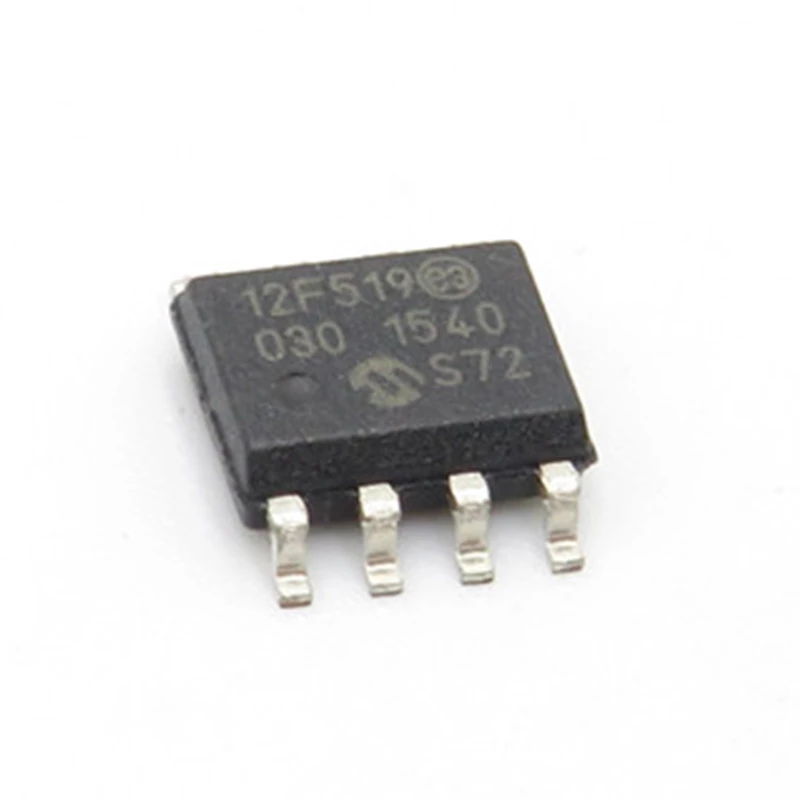
Break IC PIC12F519 Binary
Break IC PIC12F519 Binary will begin from unlock microprocessor pic12f519 eeprom and flash memory, and then readout the secured code from mcu pic12f519;
Break IC PIC12F519 Binary will begin from unlock microprocessor pic12f519 eeprom and flash memory, and then readout the secured code from mcu pic12f519
High-Performance RISC CPU:
· Only 33 Single-Word Instructions
· All Single-Cycle Instructions except for Program Branches which are Two-Cycle
· Two-Level Deep Hardware Stack
· Direct, Indirect and Relative Addressing modes for Data and Instructions
· Operating Speed:
– DC – 8 MHz Oscillator
– DC – 500 ns instruction cycle
· On-chip Flash Program Memory
– 1024 x 12
· General Purpose Registers (SRAM)
– 41 x 8
· Flash Data Memory
– 64 x 8
Special Microcontroller Features:
· 8 MHz Precision Internal Oscillator
– Factory calibrated to ±1%
· In-Circuit Serial Programming™ (ICSP™)
· In-Circuit Debugging (ICD) Support
· Power-on Reset (POR)
· Device Reset Timer (DRT)
Extrair o microchip PIC12F519 seguro MCU Flash Code precisa quebrar o bit de fusível protegido IC pic12f519 protegido e, em seguida, extrair o arquivo heximal da memória flash do microcontrolador bloqueado pic12f519
· Watchdog Timer (WDT) with Dedicated On-Chip RC Oscillator for Reliable Operation
· Programmable Code Protection
· Multiplexed MCLR Input Pin
· Internal Weak Pull-ups on I/O Pins
· Power-Saving Sleep mode
· Wake-up from Sleep on Pin Change
· Selectable Oscillator Options:
– INTRC: 4 MHz or 8 MHz precision Internal RC oscillator
– EXTRC: External low-cost RC oscillator
– XT: Standard crystal/resonator
– LP: Power-saving, low-frequency crystal
Low-Power Features/CMOS Technology:
· Standby Current:
– 100 nA @ 2.0V, typical
· Operating Current:
– 11 ìA @ 32 kHz, 2.0V, typical
– 175 ìA @ 4 MHz, 2.0V, typical
· Watchdog Timer Current:
– 1 ìA @ 2.0V, typical
– 7 ìA @ 5.0V, typical
· High Endurance Program and Flash Data Memory Cells
quebrar microcontrolador bloqueado PIC12F519 bit de fusível de segurança e leitura heximal embutido do microprocessador seguro pic12f519, programa binário original do clone para a nova unidade MCU pic12f519;
– 100,000 write Program Memory endurance
– 1,000,000 write Flash Data Memory endurance
– Program and Flash Data retention: >40 years
· Fully Static Design
· Wide Operating Voltage Range: 2.0V to 5.5V
– Wide temperature range
– Industrial: -40°C to +85°C
– Extended: -40°C to +125°C
Peripheral Features:
· 6 I/O Pins
– 5 I/O pins with individual direction control
– High current sink/source for direct LED drive
· 8-bit Real-Time Clock/Counter (TMR0) with 8-bit Programmable Prescaler.
The PIC12F519 device from Microchip Technology is low-cost, high-performance, 8-bit, fully-static, Flash-based CMOS microcontrollers. They employ a RISC architecture with only 33 single-word/single-cycle instructions. All instructions are single cycle except for program branches, which take two cycles when Break IC.
The PIC12F519 device delivers performance an order of magnitude higher than their competitors in the same price category. The 12-bit wide instructions are highly symmetrical, resulting in a typical 2:1 code compression over other 8-bit microcontrollers in its class. The easy-to-use and easy to remember instruction set reduces development time significantly.
The PIC12F519 product is equipped with special features that reduce system cost and power requirements. The Power-on Reset (POR) and Device Reset Timer (DRT) eliminate the need for external Reset circuitry. There are four oscillator configurations to choose from including INTRC Internal Oscillator mode and the power-saving LP (Low-power) Oscillator mode.
Power-Saving Sleep mode, Watchdog Timer and code protection features improve system cost, power and reliability. The PIC12F519 device is available in the cost-effective Flash programmable version, which is suitable for production in any volume. The customer can take full advantage of Microchip’s price leadership in Flash programmable microcontrollers, while benefiting from the Flash programmable flexibility.
The PIC12F519 product is supported by a full-featured macro assembler, a software simulator, an in-circuit emulator, a low-cost development programmer and a full featured programmer. All the tools are supported on PC and compatible machines.
Break IC ATMEGA261P Flash
We can Break IC ATMEGA261P Flash, please view the IC ATMEGA261P features for your reference:
The N variable represents the prescale factor (1, 8, 32, 64, 128, 256, or 1024). The extreme values for the OCR2A Register represent special cases when generating a PWM waveform output in the phase correct PWM mode. If the OCR2A is set equal to BOTTOM, the output will be continuously low and if set equal to MAX the output will be continuously high for non-inverted PWM mode. For inverted PWM the output will have the opposite logic values if Break IC flash.
At the very start of period 2 in Figure 73 OCnx has a transition from high to low even though there is no Compare Match. The point of this transition is to guarantee symmetry around BOTTOM. There are two cases that give a transition without Compare Match.
OCR2A changes its value from MAX, like in Figure 73. When the OCR2A value is MAX the OCn pin value is the same as the result of a down-counting compare match. To ensure symmetry around BOTTOM the OCn value at MAX must correspond to the result of an up-counting Compare Match after Break IC flash.
The timer starts counting from a value higher than the one in OCR2A, and for that reason misses the Compare Match and hence the OCn change that would have happened on the way up. The following figures show the Timer/Counter in synchronous mode, and the timer clock (clkT2) is therefore shown as a clock enable signal. In asynchronous mode, clkI/O should be replaced by the Timer/Counter Oscillator clock before Break IC flash.
The figures include information on when Interrupt Flags are set. Figure 74 contains timing data for basic Timer/Counter operation. The figure shows the count sequence close to the MAX value in all modes other than phase correct PWM mode. These bits control the Output Compare pin (OC2A) behavior. If one or both of the COM2A1:0 bits are set, the OC2A output overrides the normal port functionality of the I/O pin it is connected to. However, note that the Data Direction Register (DDR) bit corresponding to the OC2A pin must be set in order to enable the output driver if Break IC flash.
When OC2A is connected to the pin, the function of the COM2A1:0 bits depends on the WGM22:0 bit setting. Table 85 shows the COM2A1:0 bit functionality when the WGM22:0 bits are set to a normal or CTC mode (non-PWM). These bits control the Output Compare pin (OC2B) behavior. If one or both of the COM2B1:0 bits are set, the OC2B output overrides the normal port functionality of the I/O pin it is connected to. However, note that the Data Direction Register (DDR) bit corresponding to the OC2B pin must be set in order to enable the output driver after Break IC flash.
When OC2B is connected to the pin, the function of the COM2B1:0 bits depends on the WGM22:0 bit setting. Table 88 shows the COM2B1:0 bit functionality when the WGM22:0 bits are set to a normal or CTC mode (non-PWM).
Recovery MCU PIC16C662 Heximal
Recovery MCU PIC16C662 Heximal
We can Recovery MCU PIC16C662 Heximal, please view the MCU PIC16C662 features for your reference:
The clock input (from OSC1) is internally divided by four to generate four non-overlapping quadrature clocks namely Q1, Q2, Q3, and Q4. Internally, the program counter (PC) is incremented every Q1, the instruction is fetched from the program memory and latched into the instruction register in Q4. The instruction is decoded and executed during the following Q1 through Q4. The clocks and instruction execution flow is shown in Figure 3-3 if Recovery MCU.
An “Instruction Cycle” consists of four Q cycles (Q1, Q2, Q3, and Q4). The instruction fetch and execute are pipelined such that fetch takes one instruction cycle while decode and execute takes another instruction cycle. However, due to the pipelining, each instruction effectively executes in one cycle after Recovery MCU.
If an instruction causes the program counter to change (e.g., GOTO) then two cycles are required to complete the instruction (Example 3-1). A fetch cycle begins with the program counter (PC) incrementing in Q1 before Recovery MCU.
In the execution cycle, the fetched instruction is latched into the “Instruction Register (IR)” in cycle Q1. This instruction is then decoded and executed during the Q2, Q3, and Q4 cycles. Data memory is read during Q2 (operand read) and written during Q4 (destination write) if Recovery MCU.
The PIC16C64X & PIC16C66X have a 13-bit program counter capable of addressing an 8K x 14 program memory space. For the PIC16C641 and PIC16C661 only the first 2K x 14 (0000h – 07FFh) is physically implemented. For the PIC16C642 and PIC16C662 only the first 4K x 14 (0000h – 0FFh) is physically implemented before Recovery MCU.
Accessing a location above the 2K or 4K boundary will cause a wrap-around. The reset vector is at 0000h and the interrupt vector is at 0004h (Figure 4- 1 and Figure 4-2). See Section 4.4 for Program Memory paging. The data memory (Figure 4-4) is partitioned into two banks which contain the general purpose registers and the special function registers when Recovery MCU.
Bank 0 is selected when bit RP0 (STATUS<5>) is cleared. Bank 1 is selected when the RP0 bit is set. The Special Function Registers are located in the first 32 locations of each Bank before Recovery MCU.
Register locations A0h-EFh (Bank 1) are general purpose registers implemented as static RAM. Some special function registers are mapped in Bank 1. The register file is organized as 176 x 8 for the PIC16C642/662, and 128 x8 for the PIC16C641/661. Each is accessed either directly, or indirectly through the File Select Register FSR (Section 4.5) if Recovery MCU.
Reverse MCU ATMEGA261 Heximal
We can Reverse Mcu ATMEGA261 Heximal, please view the Mcu ATMEGA261 features for your reference:
The N variable represents the prescale factor (1, 8, 32, 64, 128, 256, or 1024). The extreme values for the OCR2A Register represent special cases when generating a PWM waveform output in the fast PWM mode.
If the OCR2A is set equal to BOTTOM, the output will be a narrow spike for each MAX+1 timer clock cycle. Setting the OCR2A equal to MAX will result in a constantly high or low output (depending on the polarity of the output set by the COM2A1:0 bits.) when Reverse Mcu Heximal.
A frequency (with 50% duty cycle) waveform output in fast PWM mode can be achieved by setting OC2x to toggle its logical level on each compare match (COM2x1:0 = 1). The waveform generated will have a maximum frequency of foc2 = fclk_I/O/2 when OCR2A is set to zero if Reverse Mcu Heximal.
This feature is similar to the OC2A toggle in CTC mode, except the double buffer feature of the Output Compare unit is enabled in the fast PWM mode. The phase correct PWM mode (WGM22:0 = 1 or 5) provides a high resolution phase correct PWM waveform generation option before Reverse Mcu Heximal.
The phase correct PWM mode is based on a dual-slope operation. The counter counts repeatedly from BOTTOM to TOP and then from TOP to BOTTOM. TOP is defined as 0xFF when WGM22:0 = 1, and OCR2A when MGM22:0 = 5. In non-inverting Compare Output mode, the Output Compare (OC2x) is cleared on the compare match between TCNT2 and OCR2x while upcounting, and set on the compare match while downcounting after Reverse Mcu Heximal.
In inverting Output Compare mode, the operation is inverted. The dual-slope operation has lower maximum operation frequency than single slope operation. However, due to the symmetric feature of the dual-slope PWM modes, these modes are preferred for motor control applications if Reverse Mcu Heximal.
In phase correct PWM mode the counter is incremented until the counter value matches TOP. When the counter reaches TOP, it changes the count direction. The TCNT2 value will be equal to TOP for one timer clock cycle. The timing diagram for the phase correct PWM mode is shown on Figure 73 before Reverse Mcu Heximal.
The TCNT2 value is in the timing diagram shown as a histogram for illustrating the dual-slope operation. The diagram includes non-inverted and inverted PWM outputs. The small horizontal line marks on the TCNT2 slopes represent compare matches between OCR2x and TCNT2 when Reverse Mcu Heximal.
The Timer/Counter Overflow Flag (TOV2) is set each time the counter reaches BOTTOM. The Interrupt Flag can be used to generate an interrupt each time the counter reaches the BOTTOM value. In phase correct PWM mode, the compare unit allows generation of PWM waveforms on the OC2x pin. Setting the COM2x1:0 bits to two will produce a non-inverted PWM. An inverted PWM output can be generated by setting the COM2x1:0 to three. TOP is defined as 0xFF when WGM2:0 = 3, and OCR2A when MGM2:0 = 7 (See Table 87 on page 185). The actual OC2x value will only be visible on the port pin if the data direction for the port pin is set as output if Reverse Mcu Heximal.
The PWM waveform is generated by clearing (or setting) the OC2x Register at the compare match between OCR2x and TCNT2 when the counter increments, and setting (or clearing) the OC2x Register at compare match between OCR2x and TCNT2 when the counter decrements. The PWM frequency for the output when using phase correct PWM can be calculated by the following equation.
Recover Chip PIC16C642 Binary
Recover Chip PIC16C642 Binary
We can Recover Chip PIC16C642 Binary, please view the Chip PIC16C642 features for your reference:
PIC16C64X & PIC16C66X devices are 28-pin and 40-pin EPROM-based members of the versatile PIC16CXXX family of low-cost, high-performance, CMOS, fully-static, 8-bit microcontrollers when Recover Chip. All PIC16/17 microcontrollers employ an advanced RISC architecture. The PIC16CXXX family has enhanced core features, eight-level deep stack, and multiple internal and external interrupt sources after Recover Chip.
The separate instruction and data buses of the Harvard architecture allow a 14-bit wide instruction word with the separate 8-bit wide data. The two-stage instruction pipeline allows all instructions to execute in a single-cycle, except for program branches (which require two cycles) if Recover Chip. A total of 35 instructions (reduced instruction set) are available. Additionally, a large register set gives some of the architectural innovations used to achieve a very high performance .
PIC16CXXX microcontrollers typically achieve a 2:1 code compression and a 4:1 speed improvement over other 8-bit microcontrollers in its class. The PIC16C641 has 128 bytes of RAM and the PIC16C642 has 176 bytes of RAM. Both devices have 22 I/O pins, and an 8-bit timer/counter with an 8-bit programmable prescaler when Recover Chip. In addition, they have two analog comparators with a programmable on-chip voltage reference module.
Program Memory has internal parity error detection circuitry with a Parity Error Reset. The comparator module is ideally suited for applications requiring a low-cost analog interface (e.g., battery chargers, threshold detectors, white goods controllers, etc.) before Recover Chip.
The PIC16C661 has 128 bytes of RAM and the PIC16C662 has 176 bytes of RAM. Both devices have 33 I/O pins, and an 8-bit timer/counter with an 8-bit programmable prescaler. They also have an 8-bit Parallel Slave Port. In addition, the devices have two analog comparators with a programmable on-chip voltage reference module when Recover Chip. Program Memory has internal parity error detection circuitry with a Parity Error Reset.
The comparator module is ideally suited for applications requiring a low-cost analog interface (e.g., battery chargers, threshold detectors, white goods controllers, etc.) if Recover Chip.