 Break IC PIC16F627 Code
Break IC PIC16F627 and extract flash code from mcu pic16f627, the fuse bit of microcontroller pic16f627 will be cracked by focus ion beam;
We can Break IC PIC16F627 Code, please view the IC PIC16F627 features for your reference:
High Performance RISC CPU:
· Only 35 instructions to learn
· All single-cycle instructions (200 ns), except for program branches which are two-cycle
· Operating speed:
– DC – 20 MHz clock input
– DC – 200 ns instruction cycle Interrupt capability
16 special function hardware registers
8-level deep hardware stack
Direct, Indirect and Relative addressing modes
Peripheral Features:
· 15 I/O pins with individual direction control
· High current sink/source for direct LED drive
· Analog comparator module with:
– Two analog comparators
– Programmable on-chip voltage reference (VREF) module
– Programmable input multiplexing from device inputs and internal voltage reference
– Comparator outputs are externally accessible
· Timer0: 8-bit timer/counter with 8-bit programmable prescaler
· Timer1: 16-bit timer/counter with external crystal/ clock capability
· Timer2: 8-bit timer/counter with 8-bit period register, prescaler and postscaler
· Capture, Compare, PWM (CCP) module
– Capture is 16-bit, max. resolution is 12.5 ns
– Compare is 16-bit, max. resolution is 200 ns
– PWM max. resolution is 10-bit
· Universal Synchronous/Asynchronous Receiver/Transmitter USART/SCI
· 16 Bytes of common RAM
Special Microcontroller Features:
· Power-on Reset (POR)
· Power-up Timer (PWRT) and Oscillator Start-up Timer (OST)
· Brown-out Detect (BOD)
· Watchdog Timer (WDT) with its own on-chip RC oscillator for reliable operation
· Multiplexed MCLR-pin
· Programmable weak pull-ups on PORTB
· Programmable code protection
· Low voltage programming
· Power saving SLEEP mode
· Selectable oscillator options
– FLASH configuration bits for oscillator options
– ER (External Resistor) oscillator
– Reduced part count
– Dual speed INTRC
– Lower current consumption
– EC External Clock input
– XT oscillator mode
– HS oscillator mode
– LP oscillator mode
· Serial in-circuit programming (via two pins)
· Four user programmable ID locations
CMOS Technology:
· Low-power, high-speed CMOS FLASH technology
· Fully static design
· Wide operating voltage range
– PIC16F627 – 3.0V to 5.5V
– PIC16F628 – 3.0V to 5.5V
– PIC16LF627 – 2.0V to 5.5V
– PIC16LF628 – 2.0V to 5.5V
· Commercial, industrial and extended temperature range
· Low power consumption
– < 2.0 mA @ 5.0V, 4.0 MHz
– 15 µA typical @ 3.0V, 32 kHz
– < 1.0 µA typical standby current @ 3.0V
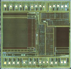
Break ic flash ATMEGA461P Flash
We can Break ic flash ATMEGA461P Flash, please view the IC ATMEGA461P features for your reference:
The SPI Data Register is a read/write register used for data transfer between the Register File and the SPI Shift Register. Writing to the register initiates data transmission when Break ic flash.
Reading the register causes the Shift Register Receive buffer to be read. There are four combinations of SCK phase and polarity with respect to serial data, which are determined by control bits CPHA and CPOL. The SPI data transfer formats are shown in Figure 81 and Figure 82 if Break ic flash.
Data bits are shifted out and latched in on opposite edges of the SCK signal, ensuring sufficient time for data signals to stabilize. This is clearly seen by summarizing Table 94 and Table 95, as done below before Break ic flash:
The Universal Synchronous and Asynchronous serial Receiver and Transmitter (USART) is a highly flexible serial communication device. The main features are:
Full Duplex Operation (Independent Serial Receive and Transmit Registers)
Asynchronous or Synchronous Operation
Master or Slave Clocked Synchronous Operation
High Resolution Baud Rate Generator
Supports Serial Frames with 5, 6, 7, 8, or 9 Data Bits and 1 or 2 Stop Bits
Odd or Even Parity Generation and Parity Check Supported by Hardware if Break ic flash
Data OverRun Detection
Framing Error Detection
Noise Filtering Includes False Start Bit Detection and Digital Low Pass Filter
Three Separate Interrupts on TX Complete, TX Data Register Empty and RX Complete
Multi-processor Communication Mode
Double Speed Asynchronous Communication ModeThe ATmega461p has four USART’s, USART0, USART1, USART2, and USART3. The functionality for all four USART’s is described below Break ic flash.
USART0, USART1, USART2, and USART3 have different I/O registers as shown in “Register Summary” on page 385.
A simplified block diagram of the USART Transmitter is shown in Figure 83 on page after Break ic flash
CPU accessible I/O Registers and I/O pins are shown in bold.
The Power Reducion USART0 bit, PRUSART0, in “Power Reduction Register 0 PRR0” on page 54 must be disabled by writing a logical zero to it when Break ic flash.
The Power Reducion USART1 bit, PRUSART1, in “Power Reduction Register 1 – PRR1” on page 55 must be disabled by writing a logical zero to it.
The Power Reducion USART2 bit, PRUSART2, in “Power Reduction Register 1 – PRR1” on page 55 must be disabled by writing a logical zero to it if Break ic flash.
The Power Reducion USART3 bit, PRUSART3, in “Power Reduction Register 1 – PRR1” on page 55 must be disabled by writing a logical zero to it.
Recovery MCU PIC12CE673 Flash
Recovery MCU PIC12CE673 Flash memory protective content, the security fuse bit of microcontroller pic12ce673 will be cracked in order to readout the embedded heximal from mcu memory;
The PIC12C67X series fits perfectly in applications ranging from personal care appliances and security systems to low-power remote transmitters/receivers.
The EPROM technology makes customizing application programs (transmitter codes, appliance settings, receiver frequencies, etc.) extremely fast and convenient, while the EEPROM data memory (PIC12CE67X only) technology allows for the changing of calibration factors and security codes after breaking IC by brutel force.
The small footprint packages, for through hole or surface mounting, make this mcu series perfect for applications with space limitations. Low-cost, low-power, high performance, ease of use and I/O flexibility make the PIC12C67X series very versatile even in areas where no mcu use has been considered before (i.e., timer functions, replacement of “glue” logic and PLD’s in larger systems, coprocessor applications).
The PIC12C67X products are compatible with other members of the 14-bit PIC16CXXX families. The PIC12C67X devices are supported by a full featured macro assembler, a software simulator, an in-circuit emulator, a low-cost development programmer and a full-featured programmer.
A “C” compiler and fuzzy logic support tools are also available. A variety of frequency ranges and packaging options are available. Depending on application and production requirements, the proper device option can be selected using the information in the PIC12C67X Product Identification System section at the end of this data sheet when Recovery Mcu.
When placing orders, please use that page of the data sheet to specify the correct part number. For example, the PIC12C67X device “type” is indicated in the device number:
1. C, as in PIC12C671. These devices have EPROM type memory and operate over the standard voltage range.
2. LC, as in PIC12LC671. These devices have EPROM type memory and operate over an extended voltage range.
3. CE, as in PIC12CE674. These devices have EPROM type memory, EEPROM data memory and operate over the standard voltage range.
4. LCE, as in PIC12LCE674. These devices have EPROM type memory, EEPROM data memory and operate over an extended voltage range.
Recover Microcontroller ATmega461PA Archive
Recover Microcontroller ATmega461PA Archive from locked flash memory and readout the atmega461pa mcu program, rewrite it to new MCU atmega461pa for cloning;
When the SPI is enabled, the data direction of the MOSI, MISO, SCK, and SS pins is overridden according to Table 93. For more details on automatic port overrides.
The following code examples show how to initialize the SPI as a Master and how to perform a simple transmission. DDR_SPI in the examples must be replaced by the actual Data Direction Register controlling the SPI pins.
DD_MOSI, DD_MISO and DD_SCK must be replaced by the actual data direction bits for these pins. E.g. if MOSI is placed on pin PB5, replace DD_MOSI with DDB5 and DDR_SPI with DDRB. When the SPI is configured as a Slave, the Slave Select (SS) pin is always input. When SS is held low, the SPI is activated, and MISO becomes an output if configured so by the user after Reverse engineering attiny4313 Microcontroller code.
All other pins are inputs. When SS is driven high, all pins are inputs, and the SPI is passive, which means that it will not receive incoming data. Note that the SPI logic will be reset once the SS pin is driven high. The SS pin is useful for packet/byte synchronization to keep the slave bit counter synchronous with the master clock generator. When the SS pin is driven high, the SPI slave will immediately reset the send and receive logic, and drop any partially received data in the Shift Register.
When the SPI is configured as a Master (MSTR in SPCR is set), the user can determine the direction of the SS pin. If SS is configured as an output, the pin is a general output pin which does not affect the SPI system. Typically, the pin will be driving the SS pin of the SPI Slave.
If SS is configured as an input, it must be held high to ensure Master SPI operation. If the SS pin is driven low by peripheral circuitry when the SPI is configured as a Master with the SS pin defined as an input, the SPI system interprets this as another master selecting the SPI as a slave and starting to send data to it. To avoid bus contention, the SPI system takes the following actions if Recover attiny2313a Microcontroller heximal:
The MSTR bit in SPCR is cleared and the SPI system becomes a Slave. As a result of the SPI becoming a Slave, the MOSI and SCK pins become inputs. The SPIF Flag in SPSR is set, and if the SPI interrupt is enabled, and the I-bit in SREG is set, the interrupt routine will be executed.
Thus, when interrupt-driven SPI transmission is used in Master mode, and there exists a possibility that SS is driven low, the interrupt should always check that the MSTR bit is still set. If the MSTR bit has been cleared by a slave select, it must be set by the user to re-enable SPI Master mode.
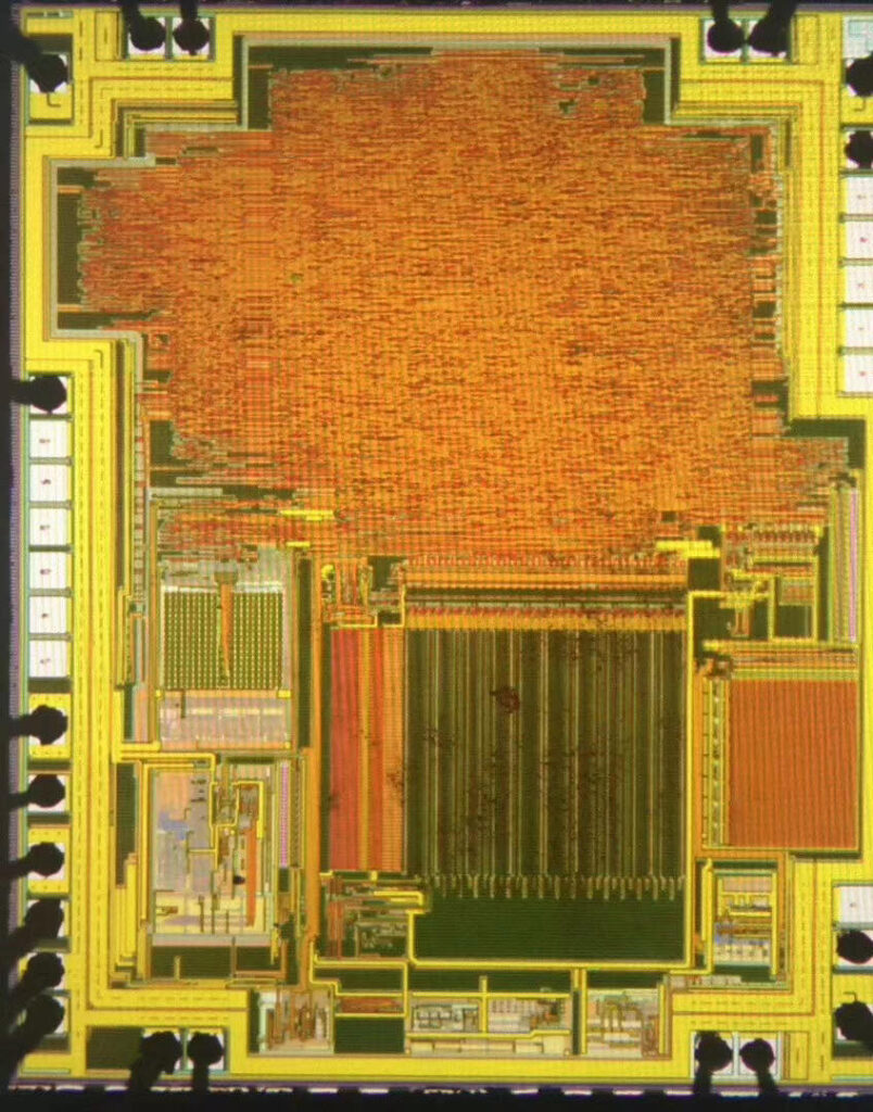
Reverse MCU ATmega461PV Binary
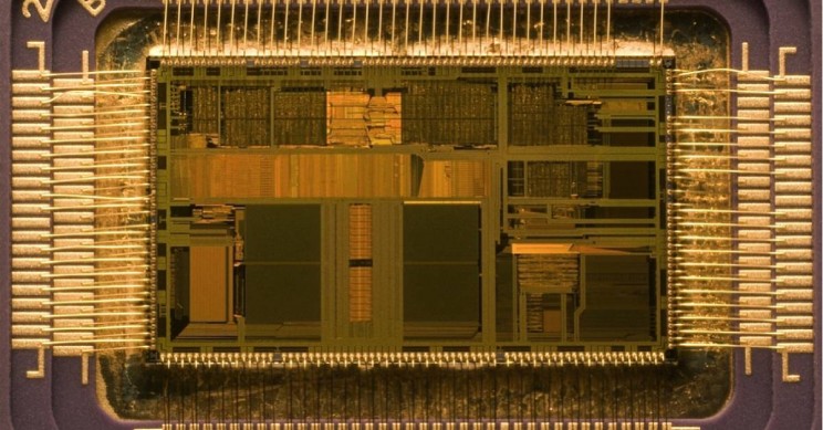
Reverse MCU ATmega461PV and readout microcontroller atmega461pv secured Binary, crack mcu protective system and using focus ion beam to cut off the security fuse bit;
The interconnection between Master and Slave CPUs with SPI is shown in Figure 80. The system consists of two shift Registers, and a Master clock generator. Th e SPI Master initiates the communication cycle when pulling low the Slave Select SS pin of the desired Slave.
Master and Slave prepare the data to be sent in their respective shift Registers, and the Master generates the required clock pulses on the SCK line to interchange data if break atmega64pa MCU binary.
Data is always shifted from Master to Slave on the Master Out – Slave In, MOSI, line, and from Slave to Master on the Master In – Slave Out, MISO, line. After each data packet, the Master will synchronize the Slave by pulling high the Slave Select, SS, line.
When configured as a Master, the SPI interface has no automatic control of the SS line. This must be handled by user software before communication can start. When this is done, writing a byte to the SPI Data Register starts the SPI clock generator, and the hardware shifts the eight bits into the Slave. After shifting one byte, the SPI clock generator stops, setting the end of Transmission Flag (SPIF) after break atmega128a MCU firmware.
If the SPI Interrupt Enable bit (SPIE) in the SPCR Register is set, an interrupt is requested. The Master may continue to shift the next byte by writing it into SPDR, or signal the end of packet by pulling high the Slave Select, SS line. The last incoming byte will be kept in the Buffer Register for later use. When configured as a Slave, the SPI interface will remain sleeping with MISO tri-stated as long as the SS pin is driven high. In this state, software may update the contents of the SPI Data Register, SPDR, bu t the data will not be shifted out by incoming clock pulses on the SCK pin until the SS pin is driven low.
As one byte has been completely shifted, the end of Transmission Flag, SPIF is set. If the SPI Interrupt Enable bit, SPIE, in the SPCR Register is set, an interrupt is requested.
The Slave may continue to place new data to be sent into SPDR before reverseing the incoming data. The last incoming byte will be kept in the Buffer Register for later use. The system is single buffered in the transmit direction and double buffered in the receive direction. This means that bytes to be transmitted cannot be written to the SPI Data Register before the entire shift cycle is completed.
When receiving data, however, a received character must be reverse from the SPI Data Register before the next character has been completely shifted in. Otherwise, the first byte is lost.
In SPI Slave mode, the control logic will sample the incoming signal of the SCK pin. To ensure correct sampling of the clock signal, the frequency of the SPI clock should never exceed fosc/4.
Recovery Microcontroller PIC16F877 Program
Recovery Microcontroller PIC16F877 Program from embedded flash and eeprom memory, the firmware of locked mcu pic16f877 will be cloned after extract microchip pic16f877 code.
PORTC is an 8-bit wide, bi-directional port. The corresponding data direction register is TRISC. Setting a TRISC bit (= 1) will make the corresponding PORTC pin an input (i.e., put the corresponding output driver in a Hi-Impedance mode). Clearing a TRISC bit (= 0) will make the corresponding PORTC pin an output (i.e., put the contents of the output latch on the selected pin).
PORTC is multiplexed with several peripheral functions When the I2C module is enabled, the PORTC<4:3> pins can be configured with normal I2C levels, or with SMBus levels by using the CKE bit (SSPSTAT<6>).
When enabling peripheral functions, care should be taken in defining TRIS bits for each PORTC pin. Some peripherals override the TRIS bit to make a pin an output, while other peripherals override the TRIS bit to make a pin an input if extract avr ic Microcontroller.
Since the TRIS bit override is in effect while the peripheral is enabled, recovery-modify-write instructions (BSF, BCF, XORWF) with TRISC as destination, should be avoided. The user should refer to the corresponding peripheral section for the correct TRIS bit settings.
PORTE and TRISE are not implemented on the PORTE has three pins (RE0/RD/AN5, RE1/WR/AN6, and RE2/CS/AN7) which are individually configureable as inputs or outputs. These pins have Schmitt Trigger input buffers after extract pld chip flash memory.
The PORTE pins become the I/O control inputs for the microprocessor port when bit PSPMODE (TRISE<4>) is set. In this mode, the user must make certain that the TRISE<2:0> bits are set, and that the pins are configured as digital inputs. Also ensure that ADCON1 is configured for digital I/O. In this mode, the input buffers are TTL.
Register 3-1 shows the TRISE register, which also controls the parallel slave port operation. PORTE pins are multiplexed with analog inputs. When selected for analog input, these pins will recovery as ’0’s. TRISE controls the direction of the RE pins, even when they are being used as analog inputs. The user must make sure to keep the pins configured as inputs when using them as analog inputs.
The Parallel Slave Port (PSP) is not implemented on the PIC16F873 or PIC16F876. PORTD operates as an 8-bit wide Parallel Slave Port or microprocessor port, when control bit PSPMODE (TRISE<4>) is set. In Slave mode, it is asynchronously recoveryable and writable by the external world through RD control input pin RE0/RD and WR control input pin RE1/WR.
The PSP can directly interface to an 8-bit microprocessor data bus. The external microprocessor can recovery or write the PORTD latch as an 8-bit latch. Setting bit PSPMODE enables port pin RE0/RD to be the RD input, RE1/WR to be the WR input and RE2/CS to be the CS (microcontroller select) input. For this functionality, the corresponding data direction bits of the TRISE register (TRISE<2:0>) must be configured as inputs (set).
The A/D port configuration bits PCFG3:PCFG0 (ADCON1<3:0>) must be set to configure pins RE2:RE0 as digital I/O. There are actually two 8-bit latches: one for data output, and one for data input. The user writes 8-bit data to the PORTD data latch and recoverys data from the port pin latch (note that they have the same address).
In this mode, the TRISD register is ignored, since the external device is controlling the direction of data flow. A write to the PSP occurs when both the CS and WR lines are first detected low. When either the CS or WR lines become high (level triggered), the Input Buffer Full (IBF) status flag bit (TRISE<7>) is set on the Q4 clock cycle, following the next Q2 cycle, to signal the write is complete (Figure 3-10).
The interrupt flag bit PSPIF (PIR1<7>) is also set on the same Q4 clock cycle. IBF can only be cleared by recoverying the PORTD input latch. The Input Buffer Overflow (IBOV) status flag bit (TRISE<5>) is set if a second write to the PSP is attempted when the previous byte has not been recovery out of the buffer.
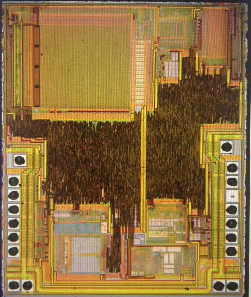
Reverse Chip ATmega461V Program
Reverse Chip ATmega461V and read mcu atmega461v flash Program, the fuse bit of atmega461v microcontroller will be broken to reset the status of MCU from locked to unlocked one;
The clock source for Timer/Counter2 is named clkT2S. clkT2S is by default connected to the main system I/O clock clkIO. By setting the AS2 bit in ASSR, Timer/Counter2 is asynchronously clocked from the TOSC1 pin.
This enables use of Timer/Counter2 as a Real Time Counter (RTC). When AS2 is set, pins TOSC1 and TOSC2 are disconnected from Port C if Reverse chip atmega861v code.
A crystal can then be connected between the TOSC1 and TOSC2 pins to serve as an independent clock source for Timer/Counter2. The Oscillator is optimized for use with a 32.768 kHz crystal. Applying an external clock source to TOSC1 is not recommended.
For Timer/Counter2, the possible prescaled selections are: clkT2S/8, clkT2S/32, clkT2S/64, clkT2S/128, clkT2S/256, and clkT2S/1024. Additionally, clkT2S as well as 0 (stop) may be selected after Reverse mcu atmega261 hex.
Setting the PSRASY bit in GTCCR resets the prescaler. This allows the user to operate with a predictable prescaler. When this bit is one, the Timer/Counter2 prescaler will be reset.
This bit is normally cleared immediately by hardware. If the bit is written when Timer/Counter2 is operating in asynchronous mode, the bit will remain one until the prescaler has been reset.
The bit will not be cleared by hardware if the TSM bit is set. Refer to the description of the “Bit 7– TSM: Timer/Counter Synchronization Mode” on page 170 for a description of the Timer/Counter Synchronization mode when Reverse CHIP PROGRAM.
The Serial Peripheral Interface (SPI) allows high-speed synchronous data transfer between the ATmega461v and peripheral devices or between several AVR devices. The ATmega640/1280/1281/2560/2561 SPI includes the following features:
Full-duplex, Three-wire Synchronous Data Transfer
Master or Slave Operation
LSB First or MSB First Data Transfer
Seven Programmable Bit Rates
End of Transmission Interrupt Flag
Write Collision Flag Protection
Wake-up from Idle Mode
Double Speed (CK/2) Master SPI Mode when Reverse CHIP PROGRAM
USART can also be used in Master SPI mode, see “USART in SPI Mode” on page 231. The Power Reduction SPI bit, PRSPI, in “Power Reduction Register 0 – PRR0” on page 54 on page 50 must be written to zero to enable SPI module.
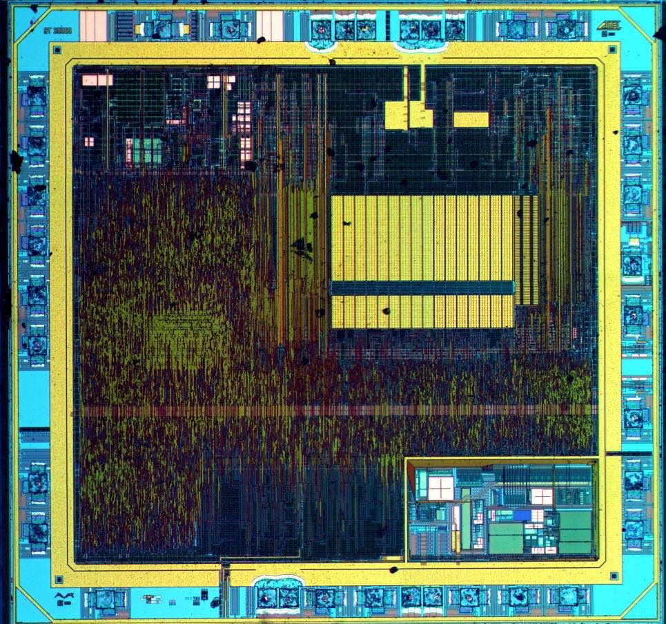
Break IC ATmega461 Eeprom
Break IC ATmega461 and read Eeprom data and flash program out from microcontroller atmega461, reprogramme heximal file into new atmega461 mcu for cloning,
If Timer/Counter2 is used to wake the device up from Power-save or ADC Noise Reduction mode, precautions must be taken if the user wants to re-enter one of these modes: The interrupt logic needs one TOSC1 cycle to be reset when recover microcontroller pic18f252 program.
If the time between wake-up and re-entering sleep mode is less than one TOSC1 cycle, the interrupt will not occur, and the device will fail to wake up. If the user is in doubt whether the time before re-entering Power-save or ADC Noise Reduction mode is sufficient, the following algorithm can be used to ensure that one TOSC1 cycle has elapsed:
Write a value to TCCR2x, TCNT2, or OCR2x.
Wait until the corresponding Update Busy Flag in ASSR returns to zero.
Enter Power-save or ADC Noise Reduction mode before Break IC.When the asynchronous operation is selected, the 32.768 kHz Oscillator for Timer/Counter2 is always running, except in Power-down and Standby modes. After a Power-up Reset or wake-up from Power-down or Standby mode, the user should be aware of the fact that this Oscillator might take as long as one second to stabilize after recover microcontroller attiny13a hex.
The user is advised to wait for at least one second before using Timer/Counter2 after power-up or wake-up from Power-down or Standby mode and The contents of all Timer/Counter2 Registers must be considered lost after a wake-up from Power-down or Standby mode due to unstable clock signal upon start-up, no matter whether the Oscillator is in use or a clock signal is applied to the TOSC1 pin.
Description of wake up from Power-save or ADC Noise Reduction mode when the timer is clocked asynchronously: When the interrupt condition is met, the wake up process is started on the following cycle of the timer clock, that is, the timer is always advanced by at least one before the processor can break the counter value.
After wake-up, the MCU is halted for four cycles, it executes the interrupt routine, and resumes execution from the instruction following SLEEP.
Breaking of the TCNT2 Register shortly after wake-up from Power-save may give an incorrect result. Since TCNT2 is clocked on the asynchronous TOSC clock, breaking TCNT2 must be done through a register synchronized to the internal I/O clock domain.
Synchronization takes place for every rising TOSC1 edge. When waking up from Power-save mode, and the I/O clock (clkI/O) again becomes active, TCNT2 will break as the previous value (before entering sleep) until the next rising TOSC1 edge.
The phase of the TOSC clock after waking up from Power-save mode is essentially unpredictable, as it depends on the wake-up time. The recommended procedure for breaking TCNT2 is thus as follows:
Write any value to either of the registers OCR2x or TCCR2x.
Wait for the corresponding Update Busy Flag to be cleared.
During asynchronous operation, the synchronization of the Interrupt Flags for the asynchronous timer takes 3 processor cycles plus one timer cycle. The timer is therefore advanced by at least one before the processor can break the timer value causing the setting of the Interrupt Flag if Break IC eeprom.
The Output Compare pin is changed on the timer clock and is not synchronized to the processor clock.
Recover Microcontroller PIC16F874 Eeprom
Recover Microcontroller PIC16F874 Eeprom content needs to unlock mcu pic16f874 secured system and read the embedded firmware from mcu pic16f874 flash memory;
We can recover MICROCONTROLLER PIC16F874 Eeprom, please view the MICROCONTROLLER PIC16F874 Eeprom features for your reference:
This document contains device specific information
Additional information may be found in the PICmicro™ Mid-Range Reference Manual (DS33023), which may be obtained from your local Microchip Sales Representative or downloaded from the Microchip website before recover MICROCONTROLLER. The Reference Manual should be considered a complementary document to this data sheet, and is highly recommended recovering for a better understanding of the device architecture and operation of the peripheral modules.
There are four devices (PIC16F873, PIC16F874, PIC16F876 and PIC16F877) covered by this datasheet. The PIC16F876/873 devices come in 28-pin packages and the PIC16F877/874 devices come in 40-pin packages. The Parallel Slave Port is not implemented on the 28-pin devices before read avr atmel mcu firmware.
The following device block diagrams are sorted by pin number; 28-pin for Figure 1-1 and 40-pin for Figure 1-2.
The 28-pin and 40-pin pinouts are listed in Table 1-1 and Table 1-2, respectively. There are three memory blocks in each of the PIC16F87X MICROCONTROLLERs. The Program Memory and Data Memory have separate buses so that concurrent access can occur and is detailed in this section. The EEPROM data memory block is detailed in Section 4.0.
Additional information on device memory may be found in the PICmicro Mid-Range Reference Manual, (DS33023). The PIC16F87X devices have a 13-bit program counter capable of addressing an 8K x 14 program memory space if recover MICROCONTROLLER. The PIC16F877/876 devices have 8K x 14 words of FLASH program memory, and the PIC16F873/874 devices have 4K x 14. Accessing a location above the physically implemented address will cause a wraparound.
The RESET vector is at 0000h and the interrupt vector is at 0004h.
Recover Microcontroller ATmega261 Heximal
Recover Microcontroller ATmega261 Heximal from embedded flash memory, the mcu atmega261 will be unlocked by focus ion beam and locked code can be extracted from atmega261 memory;
If a write is performed to any of the five Timer/Counter2 Registers while its update busy flag is set, the updated value might get corrupted and cause an unintentional interrupt to occur.
The mechanisms for reading TCNT2, OCR2A, OCR2B, TCCR2A and TCCR2B are different. When reading TCNT2, the actual timer value is read. When reading OCR2A, OCR2B, TCCR2A and TCCR2B the value in the temporary storage register is read when breaking pic12f617 microcontroller.
When Timer/Counter2 operates asynchronously, some considerations must be taken. Warning: When switching between asynchronous and synchronous clocking of Timer/Counter2, the Timer Registers TCNT2, OCR2x, and TCCR2x might be corrupted.
A safe procedure for switching clock source is:
Disable the Timer/Counter2 interrupts by clearing OCIE2x and TOIE2.
Select clock source by setting AS2 as appropriate.
Write new values to TCNT2, OCR2x, and TCCR2x.
To switch to asynchronous operation: Wait for TCN2UB, OCR2xUB, and TCR2xUB.
Clear the Timer/Counter2 Interrupt Flags.
Enable interrupts, if needed.
The CPU main clock frequency must be more than four times the Oscillator frequency.
When writing to one of the registers TCNT2, OCR2x, or TCCR2x, the value is transferred to a temporary register, and latched after two positive edges on TOSC1.
The user should not write a new value before the contents of the temporary register have been transferred to its destination. Each of the five mentioned registers have their individual temporary register, which means that e.g. writing to TCNT2 does not disturb an OCR2x write in progress when Reverse engineering pic16hv610 microcontroller program.
To detect that a transfer to the destination register has taken place, the Asynchronous Status Register – ASSR has been implemented. When entering Power-save or ADC Noise Reduction mode after having written to TCNT2, OCR2x, or TCCR2x, the user must wait until the written register has been updated if Timer/Counter2 is used to wake up the device. Otherwise, the MICROCONTROLLER will enter sleep mode before the changes are effective.
This is particularly important if any of the Output Compare2 interrupt is used to wake up the device, since the Output Compare function is disabled during writing to OCR2x or TCNT2. If the write cycle is not finished, and the MICROCONTROLLER enters sleep mode before the corresponding OCR2xUB bit returns to zero, the device will never receive a compare match interrupt, and the MICROCONTROLLER will not wake up.