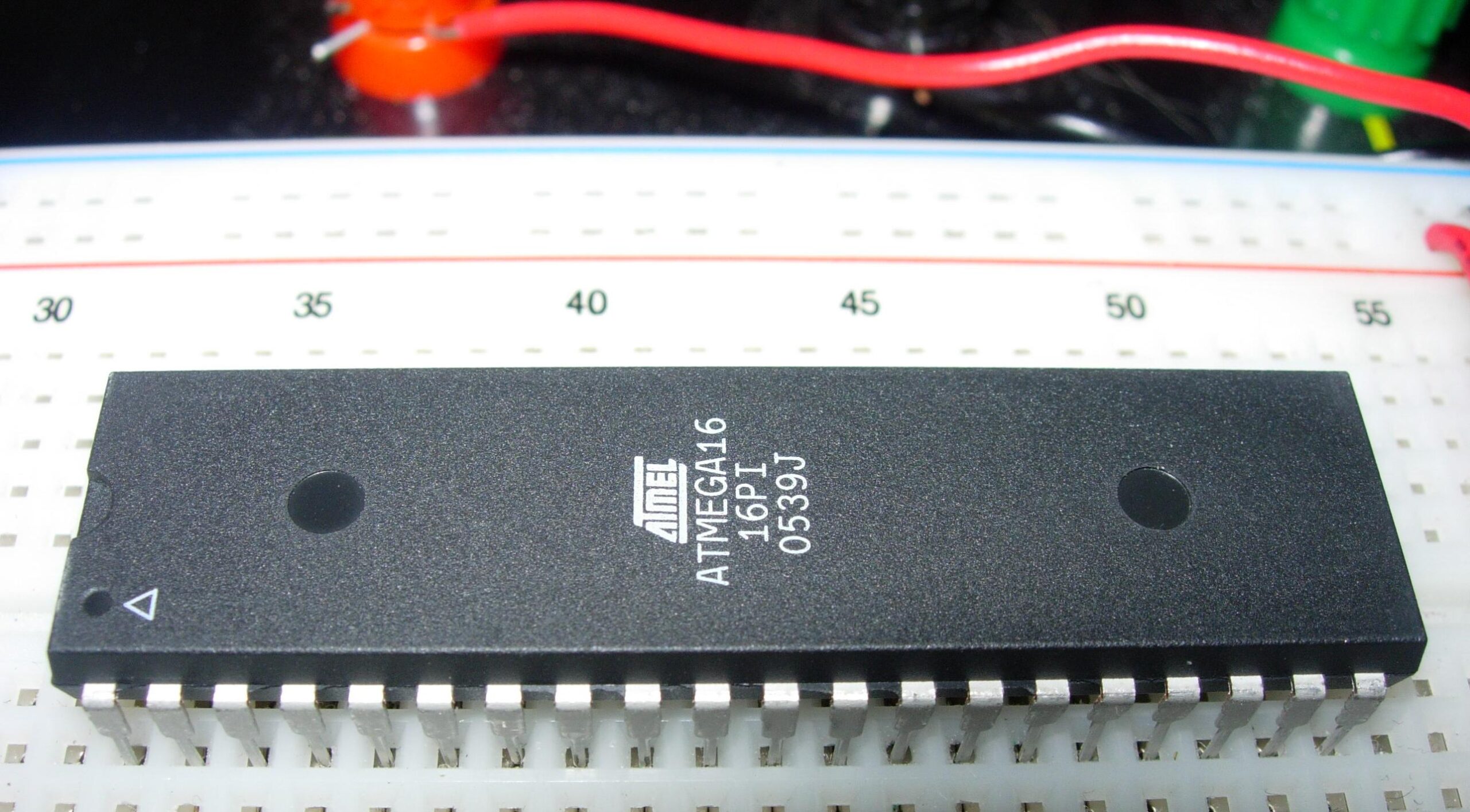
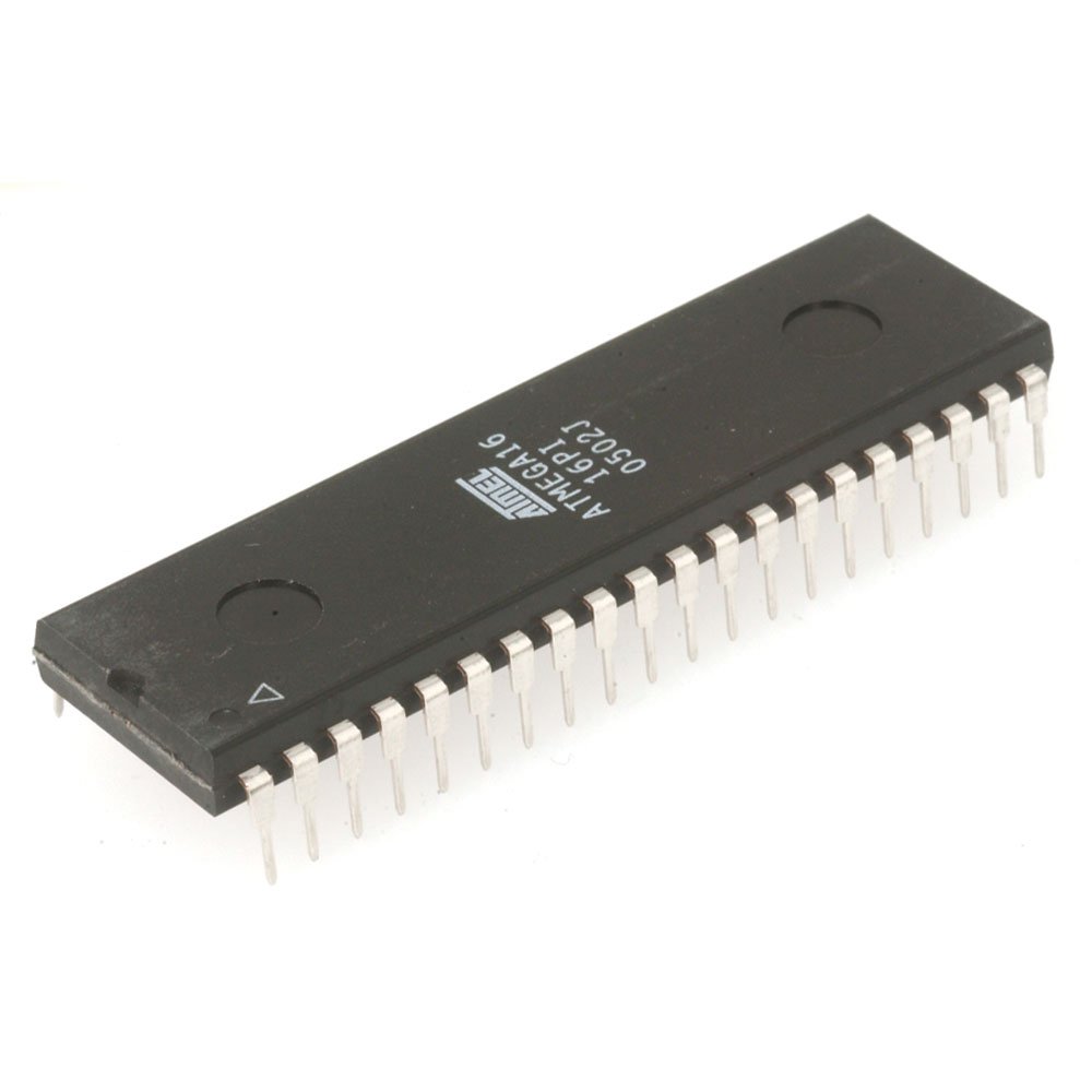
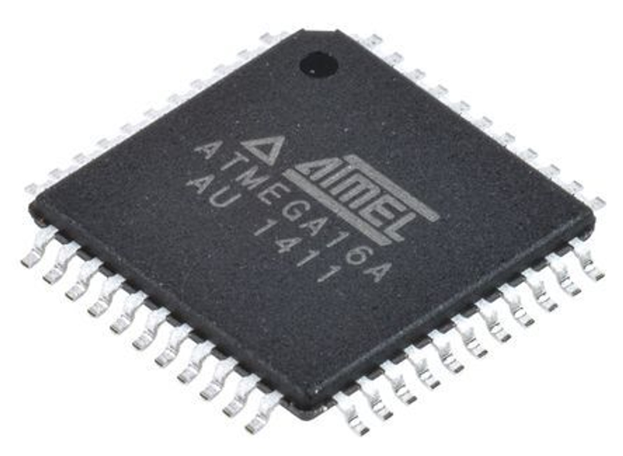
 Protective Microprocessor ATmega16 Firmware Recovery
Protective Microprocessor ATmega16 Firmware Recovery needs to crack atmega16 secured microcontroller fuse bit, read embedded heximal file out from atmega16 mcu flash and eeprom;
The lower 1120 Data memory locations address the Register File, the I/O Memory, and the internal data SRAM. The first 96 locations address the Register File and I/O Memory, and the next 1024 locations address the internal data SRAM.
crack atmega16 locked mcu fuse bit and replicate heximal data from atmega16 microprocessor flash memory
The five different addressing modes for the Data memory cover: Direct, Indirect with Displacement, Indirect, Indirect with Pre-decrement to reverse atmega8a microchip flash memory file, and Indirect with Post-increment. In the Register File, registers R26 to R31 feature the indirect addressing pointer registers.
The direct addressing reaches the entire data space.
The Indirect with Displacement mode reaches 63 address locations from the base address given by the Y- or Z- register.
attack secured atmega16 microprocessor tamper resistance and copy embedded flash program
When using register indirect addressing modes with automatic pre-decrement and post-increment, the address registers X, Y and Z are decremented or incremented.
The 32 general purpose working registers, 64 I/O Registers, and the 1024 bytes of internal data SRAM in the ATmega8A are all accessible through all these addressing modes in the process of microcontroller atmega8l flash data restoration. The Register File is described in “General Purpose Register File” on page 16.
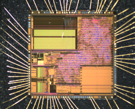
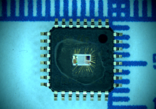
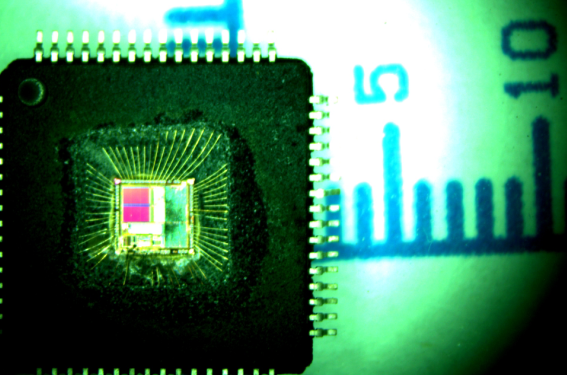
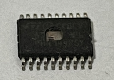
Cracking ATmega16A Microcontroller Flash Memory
Cracking ATmega16A Microcontroller Flash Memory is a process to break atmega16a mcu fuse bit, readout heximal file from microprocessor atmega16a avr chip;
When the AVR exits from an interrupt, it will always return to the main program and execute one more instruction before any pending interrupt is served.
Note that the Status Register is not automatically stored when entering an interrupt routine, nor restored when returning from an interrupt routine. This must be handled by software.
When using the CLI instruction to disable interrupts, the interrupts will be immediately disabled. No interrupt will be executed after the CLI instruction, even if it occurs simultaneously with the CLI instruction.
The following example shows how this can be used to avoid interrupts during the timed EEPROM write sequence by attacking mcu atmega162 flash memory.
rachadura ATmega16A memória flash microcontrolador é um processo para quebrar atmega16a mcu bit fusível, arquivo heximal de leitura do microprocessador atmega16a avr chip
When using the SEI instruction to enable interrupts, the instruction following SEI will be executed before any pend- ing interrupts, as shown in the following example.
The interrupt execution response for all the enabled Microchip AVR® interrupts is four clock cycles minimum. After four clock cycles, the Program Vector address for the actual interrupt handling routine is executed by break mcu atmega16a flash memory. During this 4- clock cycle period, the Program Counter is pushed onto the Stack.
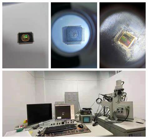
Reverse ATmega8A Microchip Memory Code
Reverse ATmega8A Microchip Memory Code needs to decode atmega8a microprocessor’s tamper resistance system, then readout MCU ATmega8a firmware from its flash and eeprom memory;
There are basically two types of interrupts. The first type is triggered by an event that sets the Interrupt Flag. For these interrupts, the Program Counter is vectored to the actual Interrupt Vector in order to execute the interrupt handling routine, and hardware clears the corresponding Interrupt Flag.
Interrupt Flags can also be cleared by writing a logic one to the flag bit position(s) to be cleared. If an interrupt condition occurs while the corresponding interrupt enable bit is cleared to duplicate avr microprocessor atmega8 protected firmware, the Interrupt Flag will be set and remembered until the interrupt is enabled, or the flag is cleared by software.
recover atmega8a mcu binary file needs to break ATmega8a microprocessor fuse bit
Similarly, if one or more interrupt conditions occur while the global interrupt enable bit is cleared, the corresponding Interrupt Flag(s) will be set and remembered until the global interrupt enable bit is set, and will then be executed by order of priority.
break ATmega8A microcontroller security fuse bit and extract source code from its flash memory
The second type of interrupts will trigger as long as the interrupt condition is present. These interrupts do not nec- essarily have Interrupt Flags. If the interrupt condition disappears before the interrupt is enabled, the interrupt will not be triggered.
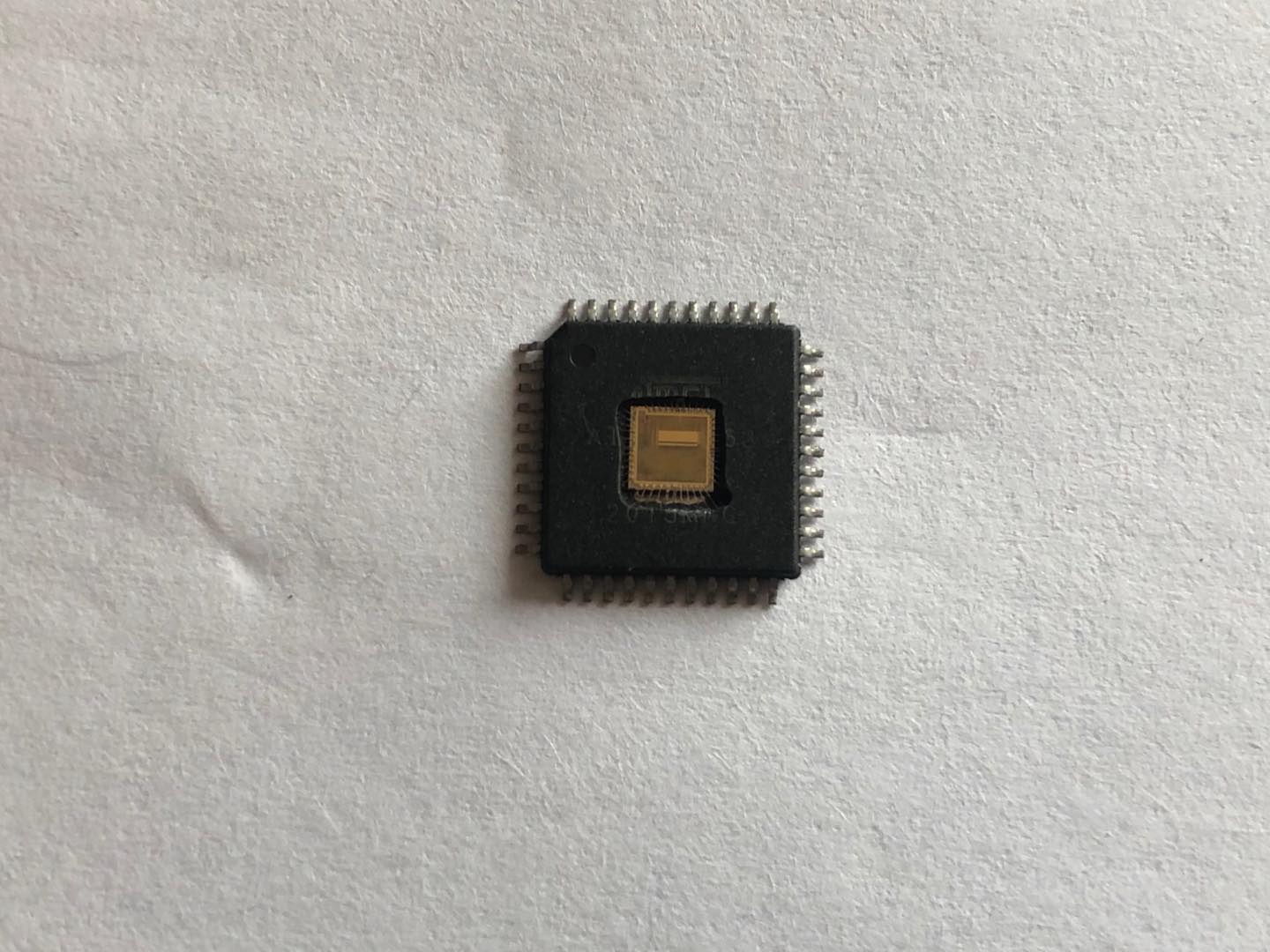
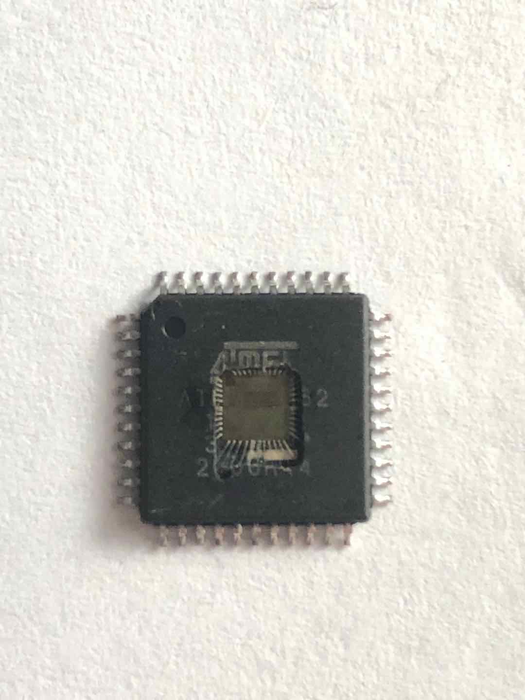
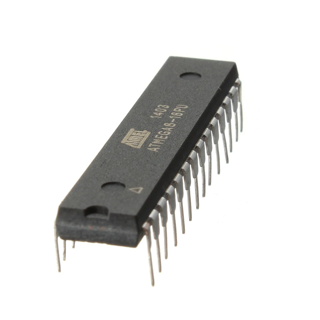
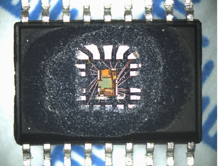
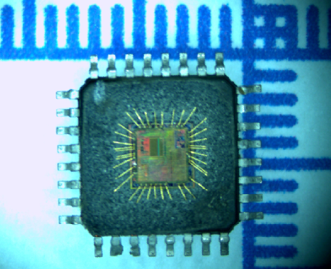
Microcontroller ATmega8L Flash Data Restoration
Microcontroller ATmega8L Flash Data Restoration is a process started from clone mcu atmega8l code from its flash memory, the embedded firmware will be readout from atmega8 microprocessor;
The Stack is effectively allocated in the general data SRAM, and consequently the Stack size is only limited by the total SRAM size and the usage of the SRAM. All user programs must initialize the SP in the reset routine (before sub-routines or interrupts are executed).
The Stack Pointer SP is read/write accessible in the I/O space. The data SRAM can easily be accessed through the five different addressing modes supported in the AVR architecture when copy mcu atmega8l heximal.
The memory spaces in the AVR architecture are all linear and regular memory maps.
microcontrolador ATmega8L restauração de dados flash é um processo iniciado a partir de clone mcu atmega8l código de sua memória flash, o firmware incorporado será lido a partir do microprocessador atmega8
A flexible interrupt module has its control registers in the I/O space with an additional global interrupt enable bit in the Status Register. All interrupts have a separate Interrupt Vector in the Interrupt Vector table.
The interrupts have priority in accordance with their Interrupt Vector position. The lower the Interrupt Vector address, the higher the priority. The I/O memory space contains 64 addresses for CPU peripheral functions as Control Registers to attack microcontroller atmega8a binary, SPI, and other I/O functions . The I/O Memory can be accessed directly, or as the Data Space locations following those of the Reg- ister File, 0x20 – 0x5F.
Microchip ATmega8 MCU Flash Content Pulling
Microchip ATmega8 MCU Flash Content Pulling will help engineer to copy avr mcu atmega8 microcontroller heximal from its flash memory, and then extract atmega8 chip binary;
The ALU supports arithmetic and logic operations between registers or between a constant and a register. Single register operations can also be executed in the ALU. After an arithmetic operation, the Status Register is updated to reflect information about the result of the operation.
The Program flow is provided by conditional and unconditional jump and call instructions, able to directly address the whole address space. Most AVR instructions have a single 16-bit word format to reverse engineering atmel microchip atmega8l firmware. Every Program memory address contains a 16- or 32-bit instruction.
Microchip ATmega8 MCU flash conteúdo puxando ajudará o engenheiro a copiar avr mcu atmega8 microcontrolador heximal de sua memória flash e, em seguida, extrair atmega8 chip binário
Program Flash memory space is divided in two sections, the Boot program section and the Application program section. Both sections have dedicated Lock Bits for write and read/write protection.
The SPM instruction that writes into the Application Flash memory section must reside in the Boot program section to copy ic atmega8l heximal file. During interrupts and subroutine calls, the return address Program Counter (PC) is stored on the Stack .
Attack Renesas R5F21244SDFP Microcontroller Protection
Attack Renesas R5F21244SDFP Microcontroller Protection and unlock microprocessor r5f21244sd flash memory, extract embedded heximal file from MCU memory;
- The measurement condition is Topr = -20 to 85°C (N version) / -40 to 85°C (D version), unless otherwise specified.
- 2. This condition (external power VCC rise gradient) does not apply if VCC ³ 1.0 V.
To use the power-on reset function, enable voltage monitor 0 reset by setting the LVD0ON bit in the OFS register to 0, the VW0C0 and VW0C6 bits in the VW0C register to 1 respectively by copying locked r5f212dasn mcu flash data, and the VCA25 bit in the VCA2 register to 1.
- When using the voltage monitor 0 digital filter, ensure that the voltage is within the MCU operation voltage range (2.2 V or above) during the sampling time.
- The sampling clock can be selected. Refer to 6. Voltage Detection Circuit of Hardware Manual for details.
Vdet0 indicates the voltage detection level of the voltage detection 0 circuit. Refer to 6. Voltage Detection Circuit of Hardware Manual for details
atacar Renesas R5F21244SDFP microcontrolador Proteção e desbloquear microprocessador r5f21244sd memória flash, extrair arquivo heximal incorporado da memória MCU;
- VCC = 2.2 to 5.5 V, Topr = -20 to 85°C (N version) / -40 to 85°C (D version), unless otherwise specified.
- 2. Standard values when the FRA1 register value after reset is assumed.
- 3. Standard values when the corrected value of the FRA6 register has been written to the FRA1 register when copying locked r5f212aasd microcontroller memory data.
This enables the setting errors of bit rates such as 9600 bps and 38400 bps to be 0% when the serial interface is used in UART mode.
Break R5F21292SDSP Locked MCU Flash Memory
Break R5F21292SDSP Locked MCU Flash Memory and clone microcontroller r5f21292 heximal file to new units which will provide the same functions as original ones;
VCC = 2.7 to 5.5 V at Topr = -20 to 85°C (N version) / -40 to 85°C (D version), unless otherwise specified.
The programming and erasure endurance is defined on a per-block basis.
If the programming and erasure endurance is n (n = 100 or 10,000), each block can be erased n times. For example, if 1,024 1-byte writes are performed to block A, a 1 Kbyte block, and then the block is erased, the programming/erasure endurance still stands at one.
However, the same address must not be programmed more than once per erase operation (overwriting prohibited).
Endurance to guarantee all electrical characteristics after program and erase. (1 to Min. value can be guaranteed).
Standard of block A and block B when program and erase endurance exceeds 1,000 times. Byte program time to 1,000 times is the same as that in program ROM.
quebrar R5F21292SDSP bloqueado MCU memória flash e clone microcontrolador r5f21292 arquivo heximal para novas unidades que irá fornecer as mesmas funções que os originais;
In a system that executes multiple programming operations, the actual erasure count can be reduced by writing to sequential addresses in turn so that as much of the block as possible is used up before performing an erase operation. For example, when programming groups of 16 bytes, the effective number of rewrites can be minimized by programming up to 128 groups before erasing them all in one operation.
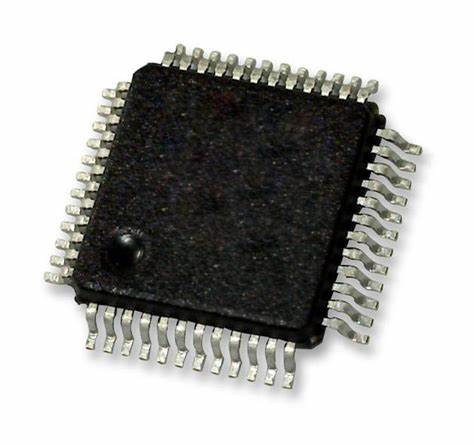
Reverse R5F21226DFP#U0 Microprocessor Binary Code
Reverse R5F21226DFP#U0 Microprocessor Binary Code and clone renesas mcu r5f21226dfp flash memory content to new MCU unit, original embedded firmware will be extracted from microcontroller flash memory;
3 circuits: XIN clock oscillation circuit (with on-chip feedback resistor),
On-chip oscillator (high-speed, low-speed)
(high-speed on-chip oscillator has a frequency adjustment function), XCIN clock oscillation circuit (32 kHz)
- Oscillation stop detection: XIN clock oscillation stop detection function
- Frequency divider circuit: Dividing selectable 1, 2, 4, 8, and 16
- Low power consumption modes:
Standard operating mode (high-speed clock, low-speed clock, high-speed on-chip oscillator, low-speed on-chip oscillator), wait mode, stop mode to copy locked r5f212dasn mcu flash data.
- External: 5 sources, Internal: 23 sources, Software: 4 sources
Priority levels: 7 levels
8 bits × 1 (with 8-bit prescaler)
reverso R5F21226DFP # U0 microprocessador código binário e clone renesas mcu r5f21226dfp conteúdo de memória flash para a nova unidade MCU, firmware incorporado original será extraído da memória flash microcontrolador
Timer mode (period timer), pulse output mode (output level inverted every period), event counter mode, pulse width measurement mode, pulse period measurement mode in the process of breaking ic mcu R5F2L388 firmware;
8 bits × 1 (with 8-bit prescaler)
Timer mode (period timer), programmable waveform generation mode (PWM output), programmable one-shot generation mode, programmable wait one- shot generation mode
Copy Locked R5F212DASNFP MCU Flash Data
Copy Locked R5F212DASNFP MCU Flash Data needs to crack RENESAS microcontroller fuse bit of flash memory, and then extract embedded firmware from microprocessor flash memory;
16 bits × 1 (with 4 capture/compare registers)
Timer mode (input capture function, output compare function), PWM mode (output 3 pins), PWM2 mode (PWM output pin)
16 bits × 2 (with 4 capture/compare registers)
Timer mode (input capture function, output compare function), PWM mode can be used for renesas locked mcu R5F212AASD memory data copying;
(output 6 pins), reset synchronous PWM mode (output three-phase waveforms (6 pins), sawtooth wave modulation), complementary PWM mode (output three-phase waveforms (6 pins), triangular wave modulation), PWM3 mode (PWM output 2 pins with fixed period)
8 bits × 1, Real-time clock mode (count seconds, minutes, hours, days of week), output compare mode
copiar dados de flash MCU R5F212DASNFP bloqueados precisa quebrar o microcontrolador RENESAS fundir bit de memória flash e, em seguida, extrair firmware incorporado da memória flash do microprocessador;
16 bits × 1 (with capture/compare register pin and compare register pin) Input capture mode, output compare mode to dump Renesas protected mcu r5f212a7sd flash program.
R8C/Tiny series core
- Number of fundamental instructions: 89
- Minimum instruction execution time:
50 ns (f(XIN) = 20 MHz, VCC = 3.0 to 5.5 V)
100 ns (f(XIN) = 10 MHz, VCC = 2.7 to 5.5 V)
200 ns (f(XIN) = 5 MHz, VCC = 2.2 to 5.5 V)
- Multiplier: 16 bits × 16 bits ® 32 bits
- Multiply-accumulate instruction: 16 bits × 16 bits + 32 bits ® 32 bits
Operation mode: Single-chip mode (address space: 1 Mbyte)
Reverse Engineer STM32F058C8 Microprocessor Heximal
Reverse Engineer STM32F058C8 Microprocessor Heximal from its secured flash memory, the fuse bit of stm32f058c8 locked MCU will be disabled and then readout its memory program;
The device has integrated power-on reset (POR) and power-down reset (PDR) circuits. They are always active, and ensure proper operation above a threshold of 2 V to reverse engineering stm32f078r8 mcu code. The device remains in reset mode when the monitored supply voltage is below a specified threshold, VPOR/PDR, without the need for an external reset circuit.
- The POR monitors only the VDD supply voltage. During the startup phase it is required that VDDA should arrive first and be greater than or equal to VDD.
- The PDR monitors both the VDD and VDDA supply voltages, however the VDDA power supply supervisor can be disabled (by programming a dedicated Option bit) to reduce the power consumption if the application design ensures that VDDA is higher than or equal to VDD.
The device features an embedded programmable voltage detector (PVD) that monitors the VDD power supply and compares it to the VPVD threshold. An interrupt can be generated when VDD drops below the VPVD threshold and/or when VDD is higher than the VPVD threshold for the sake of recovering stm32f301r6 mcu flash memory code.
engenharia reversa STM32F058C8 microprocessador heximal de sua memória flash segura, o bit de fusível de stm32f058c8 MCU bloqueado será desativado e, em seguida, ler seu programa de memória;
The interrupt service routine can then generate a warning message and/or put the MCU into a safe state. The PVD is enabled by software.