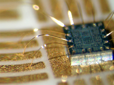
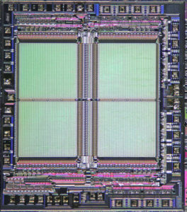
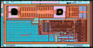
 Recover IC ATmega162PA Binary
Recover IC ATmega162PA Binary from locked memory which include flash and eeprom, extract the code from mcu atmega162pa and copy heximal to new microcontroller atmega162pa;
The USART has to be initialized before any communication can take place. The initialization process normally consists of setting the baud rate, setting frame format and enabling the Transmitter or the Receiver depending on the usage.
For interrupt driven USART operation, the Global Interrupt Flag should be cleared (and interrupts globally disabled) when doing the initialization if Reverse mcu atmega461pv IC binary.
Before doing a re-initialization with changed baud rate or frame format, be sure that there are no ongoing transmissions during the period the registers are changed. The TXCn Flag can be used to check that the Transmitter has completed all transfers, an the RXC Flag can be used to check that there are no unread data in the receive buffer.
Note that the TXCn Flag must be cleared before each transmission (before UDRn is written) if it is used for this purpose. The following simple USART initialization binary examples show one assembly and one C function that are equal in functionality.
The examples assume asynchronous operation using polling (no interrupts enabled) and a fixed frame format. The baud rate is given as a function parameter. For the assembly binary, the baud rate parameter is assumed to be stored in the r17:r16 Registers after Reverse microcontroller atmega8p archive.
More advanced initialization routines can be made that include frame format as parameters, disable interrupts and so on. However, many applications use a fixed setting of the baud and control registers, and for these types of applications the initialization binary can be placed directly in the main routine, or be combined with initialization binary for other I/O modules.
The USART Transmitter is enabled by setting the Transmit Enable (TXEN) bit in the UCSRnB Register. When the Transmitter is enabled, the normal port operation of the TxDn pin is overridden by the USART and given the function as the Transmitter’s serial output.
The baud rate, mode of operation and frame format must be set up once before doing any transmissions. If synchronous operation is used, the clock on the XCKn pin will be overridden and used as transmission clock.
Reverse Engineering Microcontroller PIC16HV610 Program
Reverse Engineering Microcontroller PIC16HV610 is a process to locate the fuse bit of mcu and unlock pic16hv610 protection, extract mcu code from pic16hv610 memory;
Reverse Engineering Microcontroller PIC16HV610 Program
We can Reverse engineering Microcontroller PIC16HV610 Program, please view the Microcontroller PIC16HV610 features for your reference:
High-Performance RISC CPU:
· Only 35 instructions to learn:
– All single-cycle instructions except branches
· Operating speed:
– DC – 20 MHz oscillator/clock input
– DC – 200 ns instruction cycle
· Interrupt capability
· 8-level deep hardware stack
· Direct, Indirect and Relative Addressing modes
Special Microcontroller Features:
· Precision Internal Oscillator:
– Factory calibrated to ±1%, typical
– User selectable frequency: 4 MHz or 8 MHz
· Power-Saving Sleep mode
· Voltage range:
– PIC16F610/616: 2.0V to 5.5V
– PIC16HV610/616: 2.0V to user defined maximum (see note)
· Industrial and Extended Temperature range
· Power-on Reset (POR)
· Power-up Timer (PWRT) and Oscillator Start-up Timer (OST)
· Brown-out Reset (BOR)
· Watchdog Timer (WDT) with independent oscillator for reliable operation before Reverse engineering Microcontroller
· Multiplexed Master Clear with pull-up/input pin
· Programmable code protection
· High Endurance Flash:
– 100,000 write Flash endurance
– Flash retention: > 40 years
Low-Power Features:
· Standby Current:
– 50 nA @ 2.0V, typical
· Operating Current:
– 20 ìA @ 32 kHz, 2.0V, typical
– 220 ìA @ 4 MHz, 2.0V, typical
· Watchdog Timer Current:
– 1 ìA @ 2.0V, typical
Peripheral Features:
· Shunt Voltage Regulator (PIC16HV610/616 only):
– 5 volt regulation
– 4 mA to 50 mA shunt range
· 11 I/O pins and 1 input only
– High current source/sink for direct LED drive
– Interrupt-on-Change pins
– Individually programmable weak pull-ups
· Analog Comparator module with:
– Two analog comparators
– Programmable on-chip voltage reference (CVREF) module (% of VDD)
– Fixed Voltage Reference
– Comparator inputs and outputs externally accessible
– SR Latch
– Built-In Hysteresis (user selectable)
· Timer0: 8-bit timer/counter with 8-bit programmable prescaler
· Enhanced Timer1:
– 16-bit timer/counter with prescaler
– External Timer1 Gate (count enable)
– Option to use OSC1 and OSC2 in LP mode as Timer1 oscillator if INTOSC mode selected
– Timer1 oscillator
· In-Circuit Serial ProgrammingTM (ICSPTM) via two pins
PIC16F616/16HV616 only:
· A/D Converter:
– 10-bit resolution
– 8 external input channels
– 2 internal reference channels
· Timer2: 8-bit timer/counter with 8-bit period register, prescaler and postscaler
· Enhanced Capture, Compare, PWM module:
– 16-bit Capture, max. resolution 12.5 ns
– 16-bit Compare, max. resolution 200 ns
– 10-bit PWM with 1, 2 or 4 output channels, programmable “dead time”, max. frequency 20 kHz
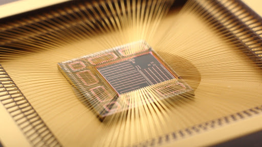
Break MCU ATmega162A Heximal
Break MCU ATmega162A and read microcontroller atmega162a memory content out from its secured flash memory, copy Heximal to new atmega162a processor as cloning;
The UCPOLn bit UCRSC selects which XCKn clock edge is used for data sampling and which is used for data change. As Figure 85 shows, when UCPOLn is zero the data will be changed at rising XCKn edge and sampled at falling XCKn edge.
If UCPOLn is set, the data will be changed at falling XCKn edge and sampled at rising XCKn edge. A serial frame is defined to be one character of data bits with synchronization bits (start and stop bits), and optionally a parity bit for error checking. The USART accepts all 30 combinations of the following as valid frame formats if recover microprocessor atmega1281pa flash memory:
1 start bit
5, 6, 7, 8, or 9 data bits
no, even or odd parity bit
1 or 2 stop bits
A frame starts with the start bit followed by the least significant data bit. Then the next data bits, up to a total of nine, are succeeding, ending with the most significant bit. If enabled, the parity bit is inserted after the data bits, before the stop bits.
When a complete frame is transmitted, it can be directly followed by a new frame, or the communication line can be set to an idle (high) state. Figure 86 illustrates the possible combinations of the frame formats. Bits inside brackets are optional.
The frame format used by the USART is set by the UCSZn2:0, UPMn1:0 and USBSn bits in UCSRnB and UCSRnC. The Receiver and Transmitter use the same setting when Break MCU ATmega2560pa heximal.
Note that changing the setting of any of these bits will corrupt all ongoing communication for both the Receiver and Transmitter.
The USART Character SiZe (UCSZn2:0) bits select the number of data bits in the frame. The USART Parity mode (UPMn1:0) bits enable and set the type of parity bit. The selection between one or two stop bits is done by the USART Stop Bit Select (USBSn) bit.
The Receiver ignores the second stop bit. An FE (Frame Error) will therefore only be detected in the cases where the first stop bit is zero. The parity bit is calculated by doing an exclusive-or of all the data bits. If odd parity is used, the result of the exclusive or is inverted. The relation between the parity bit and data bits.
If used, the parity bit is located between the last data bit and first stop bit of a serial frame.
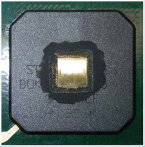
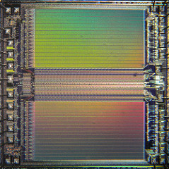
Reverse IC ATmega162P Eeprom
Reverse IC ATmega162P Eeprom after crack microcontroller atmega162p protective system, and extract locked code from mcu atmega162p flash memory;
Internal clock generation is used for the asynchronous and the synchronous master modes of operation. The description in this section refers to Figure 84. The USART Baud Rate Register (UBRRn) and the down-counter connected to it function as a programmable prescaler or baud rate generator.
The down-counter, running at system clock (fosc), is loaded with the UBRRn value each time the counter has counted down to zero or when the UBRRLn Register is written. A clock is generated each time the counter reaches zero. This clock is the baud rate generator clock output (= fosc/(UBRRn+1)). The Transmitter divides the baud rate generator clock output by 2, 8 or 16 depending on mode. The baud rate generator output is used directly by the Receiver’s clock and data recovery units after Reverse IC eeprom.
However, the recovery units use a state machine that uses 2, 8 or 16 states depending on mode set by the state of the UMSELn, U2Xn and DDR_XCKn bits. Table 98 contains equations for calculating the baud rate (in bits per second) and for calculating the UBRRn value for each mode of operation using an internally generated clock source after reverse Ic eeprom.
The transfer rate can be doubled by setting the U2Xn bit in UCSRnA. Setting this bit only has effect for the asynchronous operation. Set this bit to zero when using synchronous operation if reverse ic eeprom.
Setting this bit will reduce the divisor of the baud rate divider from 16 to 8, effectively doubling the transfer rate for asynchronous communication. Note however that the Receiver will in this case only use half the number of samples (reduced from 16 to 8) for data sampling and clock recovery, and therefore a more accurate baud rate setting and system clock are required when this mode is used. For the Transmitter, there are no downsides after Reverse IC eeprom.
External clocking is used by the synchronous slave modes of operation. The description in this section refers to Figure 84 for details. External clock input from the XCKn pin is sampled by a synchronization register to minimize the chance of meta-stability. The output from the synchronization register must then pass through an edge detector before it can be used by the Transmitter and Receiver when Reverse IC eeprom.
This process introduces a two CPU clock period delay and therefore the maximum external XCKn clock frequency is limited by the following equation when Reverse IC eeprom:
Note that fosc depends on the stability of the system clock source. It is therefore recommended to add some margin to avoid possible loss of data due to frequency variations.
When synchronous mode is used (UMSELn = 1), the XCKn pin will be used as either clock input (Slave) or clock output (Master). The dependency between the clock edges and data sampling or data change is the same. The basic principle is that data input (on RxDn) is sampled at the opposite XCKn clock edge of the edge the data output (TxDn) is changed when Reverse IC eeprom.
Break IC PIC12HV615 Heximal
Break IC PIC12HV615 Heximal
We can Break IC PIC12HV615 Heximal, please view the IC PIC12HV615 features for your reference:
To read a program memory location, the user must write two bytes of the address to the PMADRL and PMADRH registers, and then set control bit RD (PMCON1<0>). Once the read control bit is set, the program memory Flash controller will use the second instruction cycle after to read the data.
This causes the second instruction immediately following the “BSF PMCON1,RD” instruction to be ignored. The data is available in the very next cycle in the PMDATL and PMDATH registers; it can be read as two bytes in the following instructions.
PMDATL and PMDATH registers will hold this value until another read or until it is written to by the user (during a write operation). A word of the Flash program memory may only be written to if the word is in an unprotected segment of memory after Break IC.
Flash program memory must be written in four-word blocks. See Figure 3-2 and Figure 3-3 for more details. A block consists of four words with sequential addresses, with a lower boundary defined by an address, where PMADRL<1:0> = 00. All block writes to program memory are done as 16-word erase by four-word write operations. The write operation is edge aligned and cannot occur across boundaries. To write program data, it must first be loaded into the buffer registers (see Figure 3-2). This is accomplished by first writing the destination address to PMADRL and PMADRH and then writing the data to PMDATL and PMDATH.
After the address and data have been set up, then the following sequence of events must be executed:
Write 55h, then AAh, to PMCON2 (Flash programming sequence). Set the WR control bit of the PMCON1 register. All four buffer register locations should be written to with correct data. If less than four words are being written to in the block of four words, then a read from the program memory location(s) not being written to must be performed if Break IC.
This takes the data from the program location(s) not being written and loads it into the PMDATL and PMDATH registers. Then the sequence of events to transfer data to the buffer registers must be executed. To transfer data from the buffer registers to the program memory, the PMADRL and PMADRH must point to the last location in the four-word block (PMADRL<1:0> = 11). Then the following sequence of events must be executed:
Write 55h, then AAh, to PMCON2 (Flash programming sequence). Set control bit WR of the PMCON1 register to begin the write operation. The user must follow the same specific sequence to initiate the write for each word in the program block, writing each program word in sequence (000, 001, 010, 011). When the write is performed on the last word (PMADRL<1:0> = 11), a block of sixteen words is automatically erased and the content of the four-word buffer registers are written into the program memory. After the “BSF PMCON1,WR” instruction, the processor requires two cycles to set up the erase/write operation. The user must place two NOP instructions after the WR bit is set. Since data is being written to buffer registers, the writing of the first three words of the block appears to occur immediately before Break IC.
Break Chip PIC12HV609 Binary
We can Break Chip PIC12HV609 Binary, please view the Chip PIC12HV609 features for your reference:
The PIC12F609/615/617/12HV609/615 has a 13-bit program counter capable of addressing an 8K x 14 program memory space. Only the first 1K x 14 (0000h-03FFh) for the PIC12F609/615/12HV609/615 is physically implemented. For the PIC12F617, the first 2K x 14 (0000h-07FFh) is physically implemented.
Accessing a location above these boundaries will cause a wrap-around within the first 1K x 14 space for PIC12F609/615/12HV609/615 devices, and within the first 2K x 14 space for the PIC12F617 device. The Reset vector is at 0000h and the interrupt vector is at 0004h (see Figure 2-1). The data memory (see Figure 2-3) is partitioned into two banks, which contain the General Purpose Registers (GPR) and the Special Function Registers (SFR).
Special Function Registers are located in the first 32 locations of each bank. Register locations 40h-7Fh in Bank 0 are General Purpose Registers, implemented as static RAM. For the PIC12F617, the register locations 20h-7Fh in Bank 0 and
A0h-EFh in Bank 1 are general purpose registers implemented as Static RAM. Register locations F0h-FFh in Bank 1 point to addresses 70h-7Fh if Break Chip
On-chip Program Memory in Bank 0. All other RAM is unimplemented and returns ‘0’ when read. The RP0 bit of the STATUS register is the bank select bit. The register file is organized as 64 x 8 in the PIC12F609/615/12HV609/615, and as 128 x 8 in the PIC12F617. Each register is accessed, either directly or indirectly, through the File Select Register (FSR) (see Section 2.4 “Indirect Addressing, INDF and FSR Registers”).
The Special Function Registers are registers used by the CPU and peripheral functions for controlling the desired operation of the device (see Table 2-1). These registers are static RAM. The special registers can be classified into two sets: core and peripheral. The Special Function Registers associated with the “core” are described in this section when Break IC.
Those related to the operation of the peripheral features are described in the section of that peripheral feature. The STATUS register, shown in Register 2-1, contains:
· the arithmetic status of the ALU
· the Reset status
· the bank select bits for data memory (RAM)
The STATUS register can be the destination for any instruction, like any other register. If the STATUS register is the destination for an instruction that affects the Z, DC or C bits, then the write to these three bits is disabled. These bits are set or cleared according to the device logic.
Furthermore, the TO and PD bits are not writable. Therefore, the result of an instruction with the STATUS register as destination may be different than intended.
For example, CLRF STATUS, will clear the upper three bits and set the Z bit. This leaves the STATUS register as ‘000u u1uu’ (where u = unchanged).
Recover IC ATMEGA8V Firmware
We can Recover IC ATMEGA8V Firmware, please view the IC ATMEGA8V features for your reference:
On the IC ATMEGA8V devices, the DRT runs any time the device is powered up. The DRT operates on an internal oscillator. The processor is kept in Reset as long as the DRT is active when Recover IC firmware.
The DRT delay allows VDD to rise above VDD min. and for the oscillator to stabilize. The on-chip DRT keeps the devices in a Reset condition for approximately 18 ms after MCLR has reached a logic high (VIH MCLR) level if Recover IC firmware.
Programming GP3/MCLR/VPP as MCLR and using an external RC network connected to the MCLR input is not required in most cases. This allows savings in cost-sensitive and/or space restricted applications, as well as allowing the use of the GP3/MCLR/VPP pin as a general purpose input before Recover IC firmware.
The Device Reset Time delays will vary from chip-to- chip due to VDD, temperature and process variation. See AC parameters for details. Reset sources are POR, MCLR, WDT time-out and wake-up on pin change after Recover IC firmware.
See Section 9.9.2 “Wake-up from Sleep”, Notes 1, 2 and 3.
The WDT has a nominal time-out period of 18 ms, (with no prescaler). If a longer time-out period is desired, a prescaler with a division ratio of up to 1:128 can be assigned to the WDT (under software control) by writing to the OPTION register when Recover IC firmware.
Thus, a time-out period of a nominal 2.3 seconds can be realized. These periods vary with temperature, VDD and part-to-part process variations (see DC specs). Under worst-case conditions (VDD = Min., Temperature = Max., max. WDT prescaler), it may take several seconds before a WDT time-out occurs before Recover IC firmware.
9.6.2 WDT PROGRAMMING CONSIDERATIONS
The CLRWDT instruction clears the WDT and the postscaler, if assigned to the WDT, and prevents it from timing out and generating a device Reset after Recover IC firmware.
The SLEEP instruction resets the WDT and the postscaler, if assigned to the WDT. This gives the maximum Sleep time before a WDT wake-up Reset when Recover IC firmware.
Break Microcontroller PIC12F617 Binary
Break Microcontroller PIC12F617 Binary
We can Break Microcontroller PIC12F617 Binary, please view the Microcontroller PIC12F617 features for your reference:
High-Performance RISC CPU:
· Only 35 Instructions to Learn:
– All single-cycle instructions except branches
· Operating Speed:
– DC – 20 MHz oscillator/clock input
– DC – 200 ns instruction cycle
· Interrupt Capability
· 8-Level Deep Hardware Stack
· Direct, Indirect and Relative Addressing modes
Special Microcontroller Features:
· Precision Internal Oscillator:
– Factory calibrated to ±1%, typical
– Software selectable frequency: 4 MHz or 8 MHz
· Power-Saving Sleep mode
· Voltage Range:
– PIC12F609/615/617: 2.0V to 5.5V
– PIC12HV609/615: 2.0V to user defined maximum (see note)
· Industrial and Extended Temperature Range
· Power-on Reset (POR)
· Power-up Timer (PWRT) and Oscillator Start-up Timer (OST)
· Brown-out Reset (BOR)
마이크로프로세서 PIC12F617 잠금 비트를 크래킹한 후 보안 플래시 메모리에서 암호화된 MCU PIC12F617 플래시 메모리 바이너리를 복원하고 PIC12F617 잠금 마이크로컨트롤러를 새 장치로 복제합니다.
· Watchdog Timer (WDT) with independent Oscillator for Reliable Operation after Break Microcontroller
· Multiplexed Master Clear with Pull-up/Input Pin
· Programmable Code Protection
· High Endurance Flash:
– 100,000 write Flash endurance
– Flash retention: > 40 years
· Self Read/ Write Program Memory (PIC12F617 only)
Low-Power Features:
· Standby Current:
– 50 nA @ 2.0V, typical
· Operating Current:
– 11 mA @ 32 kHz, 2.0V, typical
260 mA @ 4 MHz, 2.0V, typical
· Watchdog Timer Current:
– 1 mA @ 2.0V, typical
Peripheral Features:
· Shunt Voltage Regulator (PIC12HV609/615 only):
– 5 volt regulation
– 4 mA to 50 mA shunt range
· 5 I/O Pins and 1 Input Only
· High Current Source/Sink for Direct LED Drive when Break IC
– Interrupt-on-pin change or pins
– Individually programmable weak pull-ups
· Analog Comparator module with:
Copiar Microcontrolador Bloqueado PIC12F617 Flash O programa precisa quebrar a proteção sobre a memória flash MCU PIC12F617 segura e, em seguida, extrair o arquivo heximal incorporado do processador PIC12F617;
– One analog comparator
– Programmable on-chip voltage reference (CVREF) module (% of VDD)
– Comparator inputs and output externally accessible
– Built-In Hysteresis (software selectable)
· Timer0: 8-Bit Timer/Counter with 8-Bit Programmable Prescaler
· Enhanced Timer1:
– 16-bit timer/counter with prescaler
– External Timer1 Gate (count enable)
– Option to use OSC1 and OSC2 in LP mode as Timer1 oscillator if INTOSC mode selected
– Option to use system clock as Timer1
· In-Circuit Serial ProgrammingTM (ICSPTM) via Two Pins
PIC12F615/617/HV615 ONLY:
· Enhanced Capture, Compare, PWM module:
– 16-bit Capture, max. resolution 12.5 ns
– Compare, max. resolution 200 ns
– 10-bit PWM with 1 or 2 output channels, 1 output channel programmable “dead time,” max. frequency 20 kHz, auto-shutdown
· A/D Converter:
– 10-bit resolution and 4 channels, samples internal voltage references
· Timer2: 8-Bit Timer/Counter with 8-Bit Period Register, Prescaler and Postscaler
Recover MCU PIC16F628 Firmware
Recover MCU PIC16F628 Firmware needs to unlock microcontroller pic16f628 protective memory and then readout embedded firmware from mcu pic16f628 flash memory;
We can Recover MCU PIC16F628 Firmware, please view the MCU PIC16F628 features for your reference:
The PIC16F62X are 18-Pin FLASH-based members of the versatile PIC16CXX family of low-cost, high-performance, CMOS, fully-static, 8-bit microcontrollers. All PICmicro® microcontrollers employ an advanced RISC architecture.
The PIC16F62X have enhanced core features, eight-level deep stack, and multiple internal and external interrupt sources. The separate instruction and data buses of the Harvard architecture allow a 14-bit wide instruction word with the separate 8-bit wide data.
The two-stage instruction pipeline allows all instructions to execute in a single-cycle, except for program branches (which require two cycles). A total of 35 instructions (reduced instruction set) are available. Additionally, a large register set gives some of the architectural innovations used to achieve a very high performance.
PIC16F62X microcontrollers typically achieve a 2:1 code compression and a 4:1 speed improvement over other 8-bit microcontrollers in their class. PIC16F62X devices have special features to reduce external components, thus reducing system cost, enhancing system reliability and reducing power consumption.
There are eight oscillator configurations, of which the single pin ER oscillator provides a low-cost solution. The LP oscillator minimizes power consumption, XT is a standard crystal, INTRC is a self-contained internal oscillator and the HS is for High Speed crystals.
The SLEEP (power-down) mode offers power savings. The user can wake up the chip from SLEEP through several external and internal interrupts and reset.
A highly reliable Watchdog Timer with its own on-chip RC oscillator provides protection against software lock- up.
Table 1-1 shows the features of the PIC16F62X mid-range microcontroller families. A simplified block diagram of the PIC16F62X is shown in Figure 3-1.
The PIC16F62X series fits in applications ranging from battery chargers to low-power remote sensors. The FLASH technology makes customization of application programs (detection levels, pulse generation, timers, etc.) extremely fast and convenient.
The small footprint packages make this microcontroller series ideal for all applications with space limitations. Low-cost, low-power, high-performance, ease of use and I/O flexibility make the PIC16F62X very versatile.
The PIC16F62X family is supported by a full-featured macro assembler, a software simulator, an in-circuit emulator, a low-cost development programmer and a full-featured programmer. A Third Party “C” compiler support tool is also available.
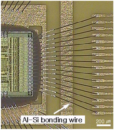
Reverse Microcontroller ATmega8P Archive
Reverse Microcontroller ATmega8P Archive needs to crack mcu atmega8p protective system and then extract locked code from mcu atmega8p flash memory;
The dashed boxes in the block diagram separate the three main parts of the USART (listed from the top): Clock Generator, Transmitter and Receiver.
Control Registers are shared by all units. The Clock Generation logic consists of synchronization logic for external clock input used by synchronous slave operation, and the baud rate generator if Recover atmega164pa MCU code.
The XCKn (Transfer Clock) pin is only used by synchronous transfer mode. The Transmitter consists of a single write buffer, a serial Shift Register, Parity Generator and Control logic for handling different serial frame formats.
The write buffer allows a continuous transfer of data without any delay between frames. The Receiver is the most complex part of the USART module due to its clock and data recovery units.
The recovery units are used for asynchronous data reception. In addition to the recovery units, the Receiver includes a Parity Checker, Control logic, a Shift Register and a two level receive buffer (UDRn).
The Receiver supports the same frame formats as the Transmitter, and can detect Frame Error, Data OverRun and Parity Errors if break microcontroller atmega324a binary.
The Clock Generation logic generates the base clock for the Transmitter and Receiver. The USARTn supports four modes of clock operation: Normal asynchronous, Double Speed asynchronous, Master synchronous and Slave synchronous mode.
The UMSELn bit in USART Control and Status Register C (UCSRnC) selects between asynchronous and synchronous operation. Double Speed (asynchronous mode only) is controlled by the U2Xn found in the UCSRnA Register.
When using synchronous mode (UMSELn = 1), the Data Direction Register for the XCKn pin (DDR_XCKn) controls whether the clock source is internal (Master mode) or external (Slave mode). The XCKn pin is only active when using synchronous mode.