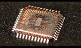
 Copy Protected Chip PIC16C56 Code
Copy Protected Chip PIC16C56 Code include program of flash and data of eeprom memory, the embedded source code of microcontroller pic16c56 will be replicated after readout frm mcu pic16c56 memory;
The PIC12C5XX device contains an 8-bit ALU and working register. The ALU is a general purpose arithmetic unit. It performs arithmetic and Boolean functions between data in the working register and any register file when attack mcu attiny2313 memory for its firmware.
The ALU is 8-bits wide and capable of addition, subtraction, shift and logical operations. Unless otherwise mentioned, arithmetic operations are two’s complement in nature.
In two-operand instructions, typically one operand is the W (working) register. The other operand is either a file register or an immediate constant before Copy avr mcu atmega165a memory.
In single operand instructions, the operand is either the W register or a file register. The W register is an 8-bit working register used for ALU operations.
It is not an addressable register. Depending on the instruction executed, the ALU may affect the values of the Carry (C), Digit Carry (DC), and Zero (Z) bits in the STATUS register.
The C and DC bits operate as a borrow and digit borrow out bit, respectively, in subtraction. See theSUBWF andADDWF instructions for examples if copy mcu atmega162 flash memory.
A simplified block diagram is shown in Figure 3-1, with the corresponding device pins described in Table 3-1. The PIC12C5XX can directly or indirectly address its register files and data memory.
All special function registers including the code counter are mapped in the data memory. The PIC12C5XX has a highly orthogonal (symmetrical) instruction set that makes it possible to carry out any operation on any register using any addressing mode. This symmetrical nature and lack of ‘special optimal situations’ make codeming with the PIC12C5XX simple yet efficient. In addition, the learning curve is reduced significantly.
Open Microcontroller PIC12LC509A Security bits
Open Microcontroller PIC12LC509A and extract embedded firmware from mcu pic12lc509a flash memory, Security bits will be decrypted to disable the protection on the microprocessor 12lc509a;
Microchip offers a unique programming service where a few user-defined locations in each device are programmed with different serial numbers when recover microcontroller stm32f105rct6 binary.
The serial numbers may be random, pseudo-random or sequential. Serial programming allows each device to have a unique number which can serve as an entry-code, password or ID number.
The high performance of the PIC12C5XX family can be attributed to a number of architectural features commonly found in RISC microprocessors.
To begin with, the PIC12C5XX uses a Harvard architecture in which program and data are accessed on separate buses. This improves bandwidth over traditional von Neumann architecture where program and data are fetched on the same bus.
Separating program and data memory further allows instructions to be sized differently than the 8-bit wide data word. Instruction opcodes are 12-bits wide making it possible to have all single word instructions when break microcontroller atmega128 heximal.
A 12-bit wide program memory access bus fetches a 12-bit instruction in a single cycle. A two-stage pipeline overlaps fetch and execution of instructions. Consequently, all instructions (33) execute in a single cycle (1µs @ 4MHz) except for program branches.
The table below lists program memory (EPROM), data memory (RAM), ROM memory, and non-volatile (EEPROM) for each device.
The PIC12C5XX can directly or indirectly address its register files and data memory. All special function registers including the program counter are mapped in the data memory. The PIC12C5XX has a highly orthogonal (symmetrical) instruction set that makes it possible to carry out any operation on any register using any addressing mode.
This symmetrical nature and lack of ‘special optimal situations’ make programming with the PIC12C5XX simple yet efficient. In addition, the learning curve is reduced significantly.
Recover IC PIC12LC508A Eeprom
Recover IC PIC12LC508A Eeprom needs to unlock mcu pic12lc508a protection and then extract the firmware from microcontroller pic12lc508a flash and eeprom memory;
A variety of packaging options are available. Depending on application and production requirements, the proper device option can be selected using the information in this section.
When placing orders, please use the PIC12C5XX Product Identification System at the back of this data sheet to specify the correct part number if copy mcu pic16c554a eeprom.
The UV erasable version, offered in ceramic side brazed package, is optimal for prototype development and pilot programs. before production shipments are available. Please contact your local Microchip Technology sales office for more details.
The UV erasable version can be erased and reprogrammed to any of the configuration modes.
Note: Please note that erasing the device will also erase the pre-programmed internal calibration value for the internal oscillator after copy microcontroller pic16c76 hex.
The calibration value must be saved prior to erasing the part. Microchip’s PICSTART® PLUS and PRO MATE® programmers all support programming of the PIC12C5XX.
Third party programmers also are available;
Microchip Third Party Guide for a list of sources. The availability of OTP devices is especially useful for customers who need the flexibility for frequent eeprom updates or small volume applications.
The OTP devices, packaged in plastic packages permit the user to program them once. In addition to the program memory, the configuration bits must also be programmed before Recover IC atmega64l eeprom.
Microchip offers a QTP Programming Service for factory production orders. This service is made available for users who choose not to program a medium to high quantity of units and whose eeprom patterns have stabilized.
The devices are identical to the OTP devices but with all EPROM locations and fuse options already programmed by the factory. Certain eeprom and prototype verification procedures do apply before production shipments are available.
Extract Chip PIC12LF510 Code
Extract Chip PIC12LF510 code from embedded flash memory, the firmware conside inside locked mcu pic12lf510 will be readout after crack microcontroller;
The PICkit™ 2 Development Programmer is a low-cost programmer with an easy-to-use interface for programming many of Microchip ’s baseline, mid-range and PIC18F families of Flash memory.
The PICkit 2 Starter Kit includes a prototyping development board, twelve sequential lessons, software and HI-TECH’s PICC™ Lite C compiler, and is designed to help get up to speed quickly using PIC® break mcu pic16f631 flash memory.
The kit provides everything needed to program, evaluate and develop applications using Microchip ’s powerful, mid-range Flash memory family.
A wide variety of demonstration, development and evaluation boards for various PIC MCUs and dsPIC DSCs allows quick application development on fully functional systems if break microcontroller pic16f628a.
Most boards include prototyping areas for adding custom circuitry and provide application firmware and source code for examination and modification after Extract Chip code.
The boards support a variety of features, including LEDs, temperature sensors, switches, speakers, RS-232 interfaces, LCD displays, potentiometers and additional EEPROM memory.
The demonstration and development boards can be used in teaching environments, for prototyping custom circuits and for learning about various Chip applications after Extract attack mcu pic16f711 hex.
In addition to the PICDEM™ and dsPICDEM™ demonstration/development board series of circuits, Microchip has a line of evaluation kits and demonstration software for analog filter design, KEELOQ® security ICs, CAN, IrDA®, PowerSmart® battery management, SEEVAL® evaluation system, Sigma-Delta ADC, flow rate sensing, plus many more.
Check the Microchip web page (www.microchip .com) and the latest “Product Selector Guide” (DS00148) for the complete list of demonstration, development and evaluation kits.
Copying Chip PIC12LF510 Program
Copying Chip PIC12LF510 Program from flash memory, the secured microcontroller will be unlocked and readout the embedded firmware heximal file from mcu pic12lf510;
The PICkit™ 2 Development Programmer is a low-cost programmer with an easy-to-use interface for programming many of Microchip’s baseline, mid-range and PIC18F families of Flash memory.
The PICkit 2 Starter Kit includes a prototyping development board, twelve sequential lessons, software and HI-TECH’s PICC™ Lite C compiler, and is designed to help get up to speed quickly using PIC® copying dsp mcu tms320lf2401avfa program.
The kit provides everything needed to program, evaluate and develop applications using Microchip’s powerful, mid-range Flash memory family of chip copying.
A wide variety of demonstration, development and evaluation boards for various PIC MCUs and dsPIC DSCs allows quick application development on fully functional systems if Copying microcontroller pic16c711 firmware.
Most boards include prototyping areas for adding custom circuitry and provide application firmware and source code for examination and modification.
The boards support a variety of features, including LEDs, temperature sensors, switches, speakers, RS-232 interfaces, LCD displays, potentiometers and additional EEPROM memory.
The demonstration and development boards can be used in teaching environments, for prototyping custom circuits and for learning about various chip applications after recover mcu pic16c73b firmware.
In addition to the PICDEM™ and dsPICDEM™ demonstration/development board series of circuits, Microchip has a line of evaluation kits and demonstration software for analog filter design, KEELOQ® security ICs, CAN, IrDA®, PowerSmart® battery management, SEEVAL® evaluation system, Sigma-Delta ADC, flow rate sensing, plus many more.
Check the Microchip web page (www.microchip.com) and the latest “Product Selector Guide” (DS00148) for the complete list of demonstration, development and evaluation kits.
Copy Chip ST10F168SQ6 Software
Copy Chip ST10F168SQ6 Software from its encrypted flash and eeprom memory, extract MCU firmware and make microcontroller st10f168sq6 cloning units;
HIGH PERFORMANCE CPU
– 16-BIT CPU WITH 4-STAGE PIPELINE
– 80ns INSTRUCTION CYCLE TIME AT 25MHz CPU CLOCK
– 400ns 16 X 16-BIT MULTIPLICATION
– 800ns 32 / 16-BIT DIVISION
– ENHANCED BOOLEAN BIT MANIPULATION FACILITIES
– ADDITIONAL INSTRUCTIONS TO SUPPORT HLL AND OPERATING SYSTEMS
– SINGLE-CYCLE CONTEXT SWITCHING SUP-
PQFP144 (28 x 28 mm) (Plastic Quad Flat Pack)
PORT A/D CONVERTER
MEMORY ORGANIZATION
– 256K BYTE ON-CHIP FLASH MEMORY
– 10K ERASING / PROGRAMMING CYCLES
– UP TO 16M BYTE LINEAR ADDRESS SPACE
FOR CODE AND DATA (5M BYTE WITH CAN) when break microcontroller s3f9454 software
– 2K BYTE ON-CHIP INTERNAL RAM (IRAM)
– 6K BYTE ON-CHIP EXTENSION RAM (XRAM)
– 20 YEAR DATA RETENTIO N TIME
FAST AND FLEXIBLE BUS
– PROGRAMMABLE EXTERNAL BUS CHARAC-
TE- RISTICS FOR DIFFERENT ADDRESS RANGES
– 8-BIT OR 16-BIT EXTERNAL DATA BUS
– MULTIPLEXED OR DEMULTIPLEXED EXTER-NAL ADDRESS / DATA BUSES
– FIVE PROGRAMMABLE CHIP-SELECT SIGNALS
– HOLD-ACKNOWLEDGE BUS ARBITRATION SUPPORT INTERRUPT
– 16-CHANNEL 10-BIT after read microchip mcu pic32mx440f512h bin
– 7.76µS CONVERSION TIME
FAIL-SAFE PROTECTIO N
– PROGRAMMABLE WATCHDOG TIMER
– OSCILLATOR WATCHDOG
ON-CHIP CAN 2.0B INTERFACE
ON-CHIP BOOTSTR AP LOADER
CLOCK GENERATION
– ON-CHIP PLL
– DIRECT OR PRESCALED CLOCK INPUT.
UP TO 111 GENERAL PURPOSE I/O LINES
– INDIVIDUALLY PROGRAMMABLE AS INPUT,
OUTPUT OR SPECIAL FUNCTION.
– PROGRAMMABLE THRESHOLD (HYSTERESIS)
IDLE AND POWER DOWN MODES
SINGLE VOLTAGE SUPPLY: 5V ±10%
144-PIN PQFP PACKAGE
Crack IC PIC12LC509 Security bits
Crack IC PIC12LC509 Security bits and decrypt microchip mcu pic12lc509 flash memory content out from it, extract secured code from pic12lc509 flash and eeprom memory in the format of heximal.
The MPLAB PM3 Device Programmer is a universal, CE compliant device programmer with programmable voltage verification at VDDMIN and VDDMAX for maximum reliability.
It features a large LCD display (128 x 64) for menus and error messages and a modular, detachable socket assembly to support various package types if recover mcu pic18f452 program.
The ICSP™ cable assembly is included as a standard item. In Stand-Alone mode, the MPLAB PM3 Device Programmer can read, verify and program PIC devices without a PC connection.
It can also set security bits protection in this mode. The MPLAB PM3 connects to the host PC via an RS-232 or USB cable.
The MPLAB PM3 has high-speed communications and optimized algorithms for quick programming of large memory devices and incorporates an SD/MMC card for file storage and secure data applications.
The PICSTART Plus Development Programmer is an easy-to-use, low-cost, prototype programmer. It connects to the PC via a COM (RS-232) port. MPLAB Integrated Development Environment software makes using the programmer simple and efficient if attack mcu tms320f241pg heximal.
The PICSTART Plus Development Programmer supports most PIC devices in DIP packages up to 40 pins. Larger pin count devices, such as the PIC16C92X and PIC17C76X, may be supported with an adapter socket.
The PICSTART Plus Development Programmer is CE compliant.
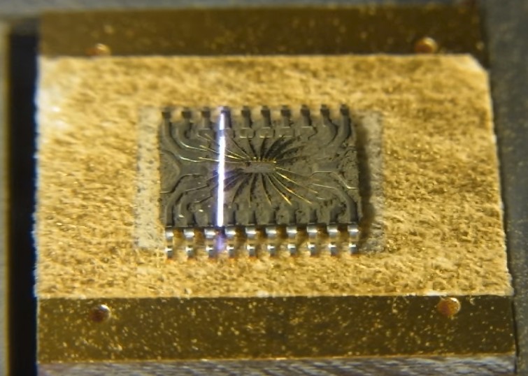
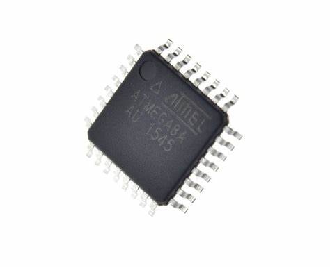
Recover IC ATmega8PA Firmware
Recover IC ATmega8PA Firmware from embedded flash and eeprom memory, the secured firmware data can be readout from atmega8pa memory, crack atmega8pa protective system by removing the security fuse bit;
The AVR core combines a rich instruction set with 32 general purpose working registers. All the 32 registers are directly connected to the Arithmetic Logic Unit (ALU), allowing two independent registers to be accessed in one single instruction executed in one clock cycle.
The resulting architecture is more code efficient while achieving throughputs up to ten times faster than conventional CISC microcontrollers. The ATmega8 provides the following features: 8K bytes of In-System Programmable Flash with Recover-While-Write capabilities, 512 bytes of EEPROM, 1K byte of SRAM, 23 general purpose I/O lines, 32 general purpose working registers, three flexible Timer/Counters with compare modes if Recover IC, internal and external interrupts, a serial programmable USART, a byte oriented Two-wire Serial Interface, a 6-channel ADC (eight channels in TQFP and QFN/MLF packages) with 10-bit accuracy, a programmable Watchdog Timer with Internal Oscillator, an SPI serial port, and five software selectable power saving modes before Reading avr chip embedded firmware.
The Idle mode stops the CPU while allowing the SRAM, Timer/Counters, SPI port, and interrupt system to continue functioning. The Power-down mode saves the register contents but freezes the Oscillator, disabling all other chip functions until the next Interrupt or Hardware Reset.
In Power-save mode, the asynchronous timer continues to run, allowing the user to maintain a timer base while the rest of the device is sleeping. The ADC Noise Reduction mode stops the CPU and all I/O modules except asynchronous timer and ADC, to minimize switching noise during ADC conversions.
In Standby mode, the crystal/resonator Oscillator is running while the rest of the device is sleeping. This allows very fast start-up combined with low-power consumption. The device is manufactured using Atmel’s high density non-volatile memory technology.
The Flash Program memory can be reprogrammed In-System through an SPI serial interface, by a conventional non-volatile memory programmer, or by an On-chip boot program running on the AVR core. The boot program can use any interface to download the application program in the Application Flash memory.
Software in the Boot Flash Section will continue to run while the Application Flash Section is updated, providing true Recover-While-Write operation. By combining an 8-bit RISC CPU with In-System Self Programmable Flash on a monolithic chip, the Atmel ATmega8 is a powerful microcontroller that provides a highly-flexible and cost-effective solution to many embedded control applications.
The ATmega8 AVR is supported with a full suite of program and system development tools, including C compilers, macro assemblers, program debugger/simulators, In-Circuit Emulators, and evaluation kits.
Reverse Chip PIC12LC508 Heximal File
Reverse Chip PIC12LC508 Heximal File is a process to replicate cpu pic12lf508 program from memory, and then extract the code from pic12lf508 locked flash memory.
A serial frame for the MSPIM is defined to be one character of 8 data bits. The USART in MSPIM mode has two valid frame formats:
8-bit data with MSB first
8-bit data with LSB first
A frame starts with the least or most significant data bit. Then the next data bits, up to a total of eight, are succeeding, ending with the most or least significant bit accordingly when attack mcu aduc831bsz firmware Heximal file.
When a complete frame is transmitted, a new frame can directly follow it, or the communication line can be set to an idle (high) state.
The UDORDn bit in UCSRnC sets the frame format used by the USART in MSPIM mode. The Receiver and Transmitter use the same setting. Note that changing the setting of any of these bits will corrupt all ongoing communication for both the Receiver and Transmitter before attack mcu tms320f28027pta CHIP.
16-bit data transfer can be achieved by writing two data bytes to UDRn. A UART transmit complete interrupt will then signal that the 16-bit value has been shifted out.
The USART in MSPIM mode has to be initialized before any communication can take place. The initialization process normally consists of setting the baud rate, setting master mode of operation (by setting DDR_XCKn to one), setting frame format and enabling the Transmitter and the Receiver.
Only the transmitter can operate independently. For interrupt driven USART operation, the Global Interrupt Flag should be cleared (and thus interrupts globally disabled) when doing the initialization.
Note:
To ensure immediate initialization of the XCKn output the baud-rate register (UBRRn) must be zero at the time the transmitter is enabled.
Contrary to the normal mode USART operation the UBRRn must then be written to the desired value after the transmitter is enabled, but before the first transmission is started after copy pic16lf877 program.
Setting UBRRn to zero before enabling the transmitter is not necessary if the initialization is done immediately after a reset since UBRRn is reset to zero.
Before doing a re-initialization with changed baud rate, data mode, or frame format, be sure that there is no ongoing transmissions during the period the registers are changed if copy mcu pic18f2480 program.
The TXCn Flag can be used to check that the Transmitter has completed all transfers, and the RXCn Flag can be used to check that there are no unread data in the receive buffer.
Note that the TXCn Flag must be cleared before each transmission (before UDRn is written) if it is used for this purpose. The following simple USART initialization heximal file examples show one assembly and one C function that are equal in functionality.
The examples assume polling (no interrupts enabled). The baud rate is given as a function parameter. For the assembly heximal file, the baud rate parameter is assumed to be stored in the r17:r16 registers.
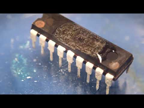
Break Chip ATmega8A Binary
Break Chip ATmega8A and extract microcontroller atmega8a Binary from its flash memory, copy mcu atmega8a heximal out and then download to the new mcu to serve as the same functionality;
First Analog Comparator conversion may be delayed
If the device is powered by a slow rising VCC, the first Analog Comparator conversion will take longer than expected on some devices. Problem Fix/Workaround, When the device has been powered or reset, disable then enable theAnalog Comparator before the first conversion.
Interrupts may be lost when writing the timer registers in the asynchronous timer If one of the timer registers which is synchronized to the asynchronous timer2 clock is written in the cycle before a overflow interrupt occurs, the interrupt may be lost if attack atmega Chip flash memory.
Problem Fix/Workaround Always check that the Timer2 Timer/Counter register, TCNT2, does not have the value 0xFF before writing the Timer2 Control Register, TCCR2, or Output Compare Register, OCR2
Signature may be Erased in Serial Programming Mode If the signature bytes are read before a chiperase command is completed, the signature may be erased causing the device ID and calibration bytes to disappear. This is critical, especially, if the part is running on internal RC oscillator.
attack ATmega8A microprocessor protective system and restore heximal file from ATmega8A mcu flash memory
Problem Fix/Workaround: Ensure that the chiperase command has exceeded before applying the next command.
CKOPT Does not Enable Internal Capacitors on XTALn/TOSCn Pins when 32 KHz Oscillator is Used to Clock the Asynchronous Timer/Counter2 When the internal RC Oscillator is used as the main clock source, it is possible to run the Timer/Counter2 asynchronously by connecting a 32 KHz Oscillator between XTAL1/TOSC1 and XTAL2/TOSC2.
But when the internal RC Oscillator is selected as the main clock source, the CKOPT Fuse does not control the internal capacitors on XTAL1/TOSC1 and XTAL2/TOSC2. As long as there are no capacitors connected to XTAL1/TOSC1 and XTAL2/TOSC2, safe operation of the Oscillator is not guaranteed if attack dsp mcu Chip flash memory.
Problem fix/Workaround
secured microcontroller atmega8a security fuse bit cracking to readout embedded program from atmega8a mcu flash memory
Use external capacitors in the range of 20 – 36 pF on XTAL1/TOSC1 and XTAL2/TOSC2. This will be fixed in ATmega8 Rev. G where the CKOPT Fuse will control internal capacitors also when internal RC Oscillator is selected as main clock source. For ATmega8 Rev. G, CKOPT = 0 (programmed) will enable the internal capacitors on XTAL1 and XTAL2. Customers who want compatibility between Rev.
G and older revisions, must ensure that CKOPT is unprogrammed (CKOPT = 1).
1
Updated Some Preliminary Test Limits and Characterization Data
The following tables have been updated:
Table 15, “Reset Characteristics,” on page 38, Table 16, “Internal Voltage Reference Characteristics,” on page 42, DC Characteristics on page 242, Table , “ADC Characteristics,” on page 248.
Changes in External Clock Frequency
Added the description at the end of “External Clock” on page 32.
Added period changing data in Table 99, “External Clock Drive,” on page 244.
Updated TWI Chapter
More details regarding use of the TWI bit rate prescaler and a Table 65, “TWI Bit
Rate Prescaler,” on page 173.
Updated Typical Start-up Times.
The following tables has been updated:
Table 5, “Start-up Times for the Crystal Oscillator Clock Selection,” on page 28,
Table 6, “Start-up Times for the Low-frequency Crystal Oscillator Clock Selection,”
on page 28, Table 8, “Start-up Times for the External RC Oscillator Clock Selection,” on page 29, and Table 12, “Start-up Times for the External Clock Selection,” on page 32 if Break Chip.