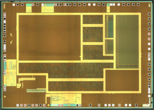
 Recover MCU ATtiny45V Program
Recover MCU ATtiny45V Program from flash and eeprom memory, unlock microcontroller attiny45v protection and readout beximal from mcu attiny45v memory;
Recover MCU ATtiny45V Program from flash and eeprom memory, unlock microcontroller attiny45v protection and readout beximal from mcu attiny45v memory
Port B is a 6-bit bi-directional I/O port with internal pull-up resistors (selected for each bit). The Port B output buffers have symmetrical drive characteristics with both high sink and source capability. As inputs, Port B pins that are externally pulled low will source current if the pull-up resistors are activated.
The Port B pins are tri-stated when a reset condition becomes active, even if the clock is not running. Reset input. A low level on this pin for longer than the minimum pulse length will generate a reset, even if the clock is not running. The minimum pulse length is given in Table 23-3 on page
170. Shorter pulses are not guaranteed to generate a reset.
A comprehensive set of development tools, application notes and datasheets are available for download on:
For compatibility with future devices, reserved bits should be written to zero if accessed. Reserved I/O memory addresses should never be written.
I/O Registers within the address range 0x00 – 0x1F are directly bit-accessible using the SBI and CBI instructions. In these registers, the value of single bits can be checked by using the SBIS and SBIC instructions.
Some of the Status Flags are cleared by writing a logical one to them. Note that, unlike most other AVRs, the CBI and SBI instructions will only operation the specified bit, and can therefore be used on registers containing such Status Flags. The CBI and SBI instructions work with registers 0x00 to 0x1F only.
PLL not locking
EEPROM recover from application code does not work in Lock Bit Mode 3
Recovering EEPROM at low frequency may not work for frequencies below 900 kHz Timer Counter 1 PWM output generation on OC1B- XOC1B does not work correctly, PLL not locking
When at frequencies below 6.0 MHz, the PLL will not lock
Problem fix / Workaround
When using the PLL, run at 6.0 MHz or higher.
EEPROM recover from application code does not work in Lock Bit Mode 3
When the Memory Lock Bits LB2 and LB1 are programmed to mode 3, EEPROM recover does not work from the application code.
Problem Fix/Work around
Do not set Lock Bit Protection Mode 3 when the application code needs to recover from EEPROM.
Recovering EEPROM at low frequency may not work for frequencies below 900 kHz, Recovering data from the EEPROM at low internal clock frequency may result in wrong data recover.
Problem Fix/Workaround
Avoid using the EEPROM at clock frequency below 900kHz. Timer Counter 1 PWM output generation on OC1B – XOC1B does not work correctly
Timer Counter1 PWM output OC1B-XOC1B does not work correctly. Only in the case when the control bits, COM1B1 and COM1B0 are in the same mode as COM1A1 and COM1A0, respectively, the OC1B-XOC1B output works correctly.
Problem Fix/Work around
The only workaround is to use same control setting on COM1A(1:0) and COM1B(1:0) control bits, see table 14-4 in the data sheet. The problem has been fixed for Tiny45 rev D.
Break PLD PALCE16V8H-15JC Software
Break PLD PALCE16V8H-15JC and extract Software from PALCE16V8 pld memory, copy JED file to new PLD chip;

We can Break PLD PALCE16V8H-15JC Software, please view below PLD PALCE16V8H-15JC features for your reference:
DISTINCTIVE CHARACTERISTICS
Pin and function compatible with all 20-pin GAL devices
Electrically erasable CMOS technology provides reconfigurable logic and full testability
High-speed CMOS technology
— 5-ns propagation delay for “-5” version
— 7.5-ns propagation delay for “-7” version
Direct plug-in replacement for the PAL16R8 series and most of the PAL10H8 series
Outputs programmable as registered or combinatorial in any combination, Peripheral Component Interconnect (PCI) compliant if recover pic16c554 software
GENERAL DESCRIPTION
The PALCE16V8 is an advanced PAL device built with low-power, high-speed, electrically-erasable CMOS technology. It is functionally compatible with all 20-pin GAL devices. The macrocells provide a universal device architecture.
The PALCE16V8 will directly replace the PAL16R8 and PAL10H8 series devices, with the excep-
tion of the PAL16C1.
The PALCE16V8 utilizes the familiar sum-of-products (AND/OR) architecture that allows users to implement complex logic functions easily and efficiently. Multiple levels of combinatorial logic can always be reduced to sum-of-products form, taking advantage of the very wide input gates available in PAL devices after recover microcontroller pic16f83 eeprom.
The equations are programmed into the device through floating gate cells in the AND logic array that can be erased electrically.
Programmable output polarity
Programmable enable/disable control
Preloadable output registers for testability
Automatic register reset on power up
Cost-effective 20-pin plastic DIP, PLCC, and SOIC packages
Extensive third-party software and programmer support through FusionPLD partners
Fully tested for 100% programming and functional yields and high reliability
5 ns version utilizes a split leadframe for improved performance.
The fixed OR array allows up to eight data product terms per output for logic functions. The sum of these products feeds the output macrocell. Each macrocell can be programmed as registered or combinatorial with an active high or active-low output after Break EPM3128ATC100 CPLD.
The output configuration is determined by two global bits and one local bit controlling four multiplexers in each macrocell.
AMD’s FusionPLD program allows PALCE16V8 designs to be implemented using a wide variety of popular industry-standard design tools. By working closely with the FusionPLD partners, AMD certifies that the tools provide accurate, quality support.
By ensuring that third party tools are available, costs are lowered because a designer does not have to buy a complete set of new tools for each device. The Fusion PLD program also greatly reduces design time since a designer can use a tool that is already installed and familiar.
Break IC ATtiny45 Heximal
Break IC ATtiny45 and readout Heximal from mcu attiny45 flash memory, unlock microcontroller attiny45 security fuse bit and remove the protection;
Port B is a 6-bit bi-directional I/O port with internal pull-up resistors (selected for each bit). The Port B output buffers have symmetrical drive characteristics with both high sink and source capability. As inputs, Port B pins that are externally pulled low will source current if the pull-up resistors are activated.
The Port B pins are tri-stated when a reset condition becomes active, even if the clock is not running. Reset input. A low level on this pin for longer than the minimum pulse length will generate a reset, even if the clock is not running.
The minimum pulse length is given in Table 23-3 on page 170. Shorter pulses are not guaranteed to generate a reset. For compatibility with future devices, reserved bits should be written to zero if accessed. Reserved I/O memory addresses should never be written. I/O Registers within the address range 0x00 – 0x1F are directly bit-accessible using the SBI and CBI instructions. In these registers, the value of single bits can be checked by using the SBIS and SBIC instructions when Break pic16f616 IC.
Some of the Status Flags are cleared by writing a logical one to them. Note that, unlike most other AVRs, the CBI and SBI instructions will only operation the specified bit, and can therefore be used on registers containing such Status Flags. The CBI and SBI instructions work with registers 0x00 to 0x1F only.
The ATTINY45 provides the following standard features:
20K bytes of Flash, 256-bytes of RAM, 32 I/O lines, three 16-bit timer/counters, a six-vector two-level interrupt architecture, a full duplex serial port, on-chip oscillator, and clock circuitry. In addition, the AT89C55 is designed with static logic for operation down to zero frequency and supports two software selectable power saving modes.
The Idle Mode stops the CPU while allowing the RAM, timer/counters, serial port, and interrupt system to continue functioning. The Power Down Mode saves the RAM contents but freezes the oscillator, disabling all other chip functions until the next hardware reset. The low-voltage option saves power and operates with a 2.7-volt power supply if Break IC.
Recover CPLD CY37256VP160-100AC Binary
We can Recover CPLD CY37256VP160-100AC Binary, please view below CPLD CY37256VP160-100AC features for your reference:
Features
· In-System Reprogrammable™ (ISR™) CMOS CPLDs
— JTAG interface for reconfigurability
— Design changes do not cause pinout changes
— Design changes do not cause timing changes when Recover CPLD
· High density
— 32 to 512 macrocells
— 32 to 264 I/O pins
— Five dedicated inputs including four clock pins
· Simple timing model
— No fanout delays
— No expander delays
— No dedicated vs. I/O pin delays
— No additional delay through PIM
— No penalty for using full 16 product terms
— No delay for steering or sharing product terms if Recover CPLD
General Description
The Ultra37000™ family of CMOS CPLDs provides a range of high-density programmable logic solutions with unparalleled
system performance. The Ultra37000 family is designed to bring the flexibility, ease of use, and performance of the 22V10 after Recover CPLD
to high-density CPLDs. The architecture is based on a number of logic blocks that are connected by a Programmable Inter-
connect Matrix (PIM). Each logic block features its own product term array, product term allocator, and 16 macrocells.
The PIM distributes signals from the logic block outputs and all input pins to the logic block inputs before Recover CPLD.
All of the Ultra37000 devices are electrically erasable and In-System Reprogrammable (ISR), which simplifies both design
and manufacturing flows, thereby reducing costs. The ISR feature provides the ability to reconfigure the devices without
having design changes cause pinout or timing changes. The Cypress ISR function is implemented through a JTAG-compliant serial interface. Data is shifted in and out through the TDI and TDO pins, respectively. Because of the superior routability and simple timing model of the Ultra37000 devices, ISR allows users to change existing logic designs while simultaneously fixing pinout assignments and maintaining system performance when Recover CPLD.
3.3V and 5V versions
PCI-compatible[1]
Programmable bus-hold capabilities on all I/Os
Intelligent product term allocator provides:
— 0 to 16 product terms to any macrocell before Recover CPLD
The entire family features JTAG for ISR and boundary scan, and is compatible with the PCI Local Bus specification,
meeting the electrical and timing requirements. The Ultra37000 family features user programmable bus-hold capabilities on all I/Os.
— Product term steering on an individual basis after Recover CPLD
— Product term sharing among local macrocells
· Flexible clocking
— Four synchronous clocks per device
— Product term clocking
— Clock polarity control per logic block
· Consistent package/pinout offering across all densities
— Simplifies design migration
— Same pinout for 3.3V and 5.0V devices if Recover MCU
· Packages
— 44 to 400 leads in PLCC, CLCC, PQFP, TQFP, CQFP,
BGA, and Fine-Pitch BGA packages
Ultra37000 5.0V Devices
The Ultra37000 devices operate with a 5V supply and can support 5V or 3.3V I/O levels. VCCO connections provide the
capability of interfacing to either a 5V or 3.3V bus. By connecting the VCCO pins to 5V the user insures 5V TTL levels on the outputs. If VCCO is connected to 3.3V the output levels meet 3.3V JEDEC standard CMOS levels and are 5V tolerant when Recover CPLD.
These devices require 5V ISR programming.
Ultra37000V 3.3V Devices
Devices operating with a 3.3V supply require 3.3V on all VCCO pins, reducing the device’s power consumption. These devices support 3.3V JEDEC standard CMOS output levels, and are 5V-tolerant. These devices allow 3.3V ISR programming before Recover CPLD.
Break MCU ATtiny25V Software
Break MCU ATtiny25V and read software from microcontroller attiny25v, the microprocessor attiny25v unlocking process will help to remove the fuse bit protection against reading flash and eeprom memory;
Port B is a 6-bit bi-directional I/O port with internal pull-up resistors (selected for each bit). The Port B output buffers have symmetrical drive characteristics with both high sink and source capability. As inputs, Port B pins that are externally pulled low will source current if the pull-up resistors are activated when recover pic16f876 Mcu.
The Port B pins are tri-stated when a reset condition becomes active, even if the clock is not running. Reset input. A low level on this pin for longer than the minimum pulse length will generate a reset, even if the clock is not running. The minimum pulse length is given in Table 23-3 on page 170. Shorter pulses are not guaranteed to generate a reset.
Some of the Status Flags are cleared by writing a logical one to them. Note that, unlike most other AVRs, the CBI and SBI before recover pic16f877 Mcu
I/O Registers within the address range 0x00 – 0x1F are directly bit-accessible using the SBI and CBI instructions. In these
For compatibility with future devices, reserved bits should be written to zero if accessed. Reserved I/O memory addresses should never be written when Break Mcu. registers, the value of single bits can be checked by using the SBIS and SBIC instructions. instructions will only operation the specified bit, and can therefore be used on registers containing such Status Flags. The CBI and SBI instructions work with registers 0x00 to 0x1F only.
PLL not locking
When at frequencies below 6.0 MHz, the PLL will not lock
Problem fix / Workaround
When using the PLL, run at 6.0 MHz or higher.
EEPROM break from application code does not work in Lock Bit Mode 3
When the Memory Lock Bits LB2 and LB1 are programmed to mode 3, EEPROM break does not work from the application code.
Problem Fix/Work around
Do not set Lock Bit Protection Mode 3 when the application code needs to break from EEPROM.
Breaking EEPROM at low frequency may not work for frequencies below 900 kHz
Breaking data from the EEPROM at low internal clock frequency may result in wrong data break.
Problem Fix/Workaround
Avoid using the EEPROM at clock frequency below 900kHz.
Timer Counter 1 PWM output generation on OC1B – XOC1B does not work correctly
Timer Counter1 PWM output OC1B-XOC1B does not work correctly. Only in the case when the control bits, COM1B1 and COM1B0 are in the same mode as COM1A1 and COM1A0, respectively, the OC1B-XOC1B output works correctly before Break Mcu.
Problem Fix/Work around
The only workaround is to use same control setting on COM1A(1:0) and COM1B(1:0) control bits, see table 14-4 in the data sheet. The problem has been fixed for Tiny45 rev D when Break Mcu.
Copy MCU PIC12C509 Program
Copy MCU PIC12C509 Program from embedded flash memory, extract code from microcontroller pic12c509 flash and eeprom memory, unlock mcu pic12c509 fuse bit by focus ion beam technique;
The high performance of the PIC12C5XX family can be attributed to a number of architectural features commonly found in RISC microprocessors.
To begin with, the PIC12C5XX uses a Harvard architecture in which program and data are accessed on separate buses.
This improves bandwidth over traditional von Neumann architecture where program and data are fetched on the same bus. Separating program and data memory further allows instructions to be sized differently than the 8-bit wide data word.
Instruction opcodes are 12-bits wide making it possible to have all single word instructions.
A 12-bit wide program memory access bus fetches a 12-bit instruction in a single cycle. A two-stage pipeline overlaps fetch and execution of instructions. Consequently, all instructions (33) execute in a single cycle (1µs @ 4MHz) except for program branches.
The table below lists program memory (EPROM), data memory (RAM), ROM memory, and non-volatile (EEPROM) for each device. The PIC12C5XX device contains an 8-bit ALU and working register. The ALU is a general purpose arithmetic unit.
It performs arithmetic and Boolean functions between data in the working register and any register file.
The ALU is 8-bits wide and capable of addition, subtraction, shift and logical operations. Unless otherwise mentioned, arithmetic operations are two’s complement in nature. In two-operand instructions, typically one operand is the W (working) register.
The other operand is either a file register or an immediate constant. In single operand instructions, the operand is either the W register or a file register.
The register is an 8-bit working register used for ALU operations. It is not an addressable register. Depending on the instruction executed, the ALU may affect the values of the Carry (C), Digit Carry (DC), and Zero (Z) bits in the STATUS register.
Th e C and DC bits operate as a borrow and digit borrow out bit, respectively, in subtraction. See theSUBWF andADDWF instructions for examples. A simplified block diagram is shown in Figure 3-1, with the corresponding device pins described in Table 3-1.
The PIC12C5XX can directly or indirectly address its register files and data memory after RECOVER MCU. All special function registers including the program counter are mapped in the data memory.
The PIC12C5XX has a highly orthogonal (symmetrical) instruction set that makes it possible to carry out any operation on any register using any addressing mode.
This symmetrical nature and lack of ‘special optimal situations’ make programming with the PIC12C5XX simple yet efficient. In addition, the learning curve is reduced significantly.
Copy IC ATmega162 Binary
Copy IC ATmega162 Binary content and unlock avr atmega162 mcu protection, and extract the embedded firmware from microcontroller atmega162 flash and eeprom memory;
High-performance, Low-power AVR® 8-bit Microcontroller
· Advanced RISC Architecture
– 131 Powerful Instructions – Most Single-clock Cycle Execution
– 32 x 8 General Purpose Working Registers
– Fully Static Operation
– Up to 16 MIPS Throughput at 16 MHz
– On-chip 2-cycle Multiplier
High Endurance Non-volatile Memory segments
– 16K Bytes of In-System Self-programmable Flash program memory
– 512 Bytes EEPROM
– 1K Bytes Internal SRAM
– Write/Erase cycles: 10,000 Flash/100,000 EEPROM
– Data retention: 20 years at 85°C/100 years at 25°C(1)
– Optional Boot Code Section with Independent Lock Bits
In-System Programming by On-chip Boot Program
True Read-While-Write Operation
– Up to 64K Bytes Optional External Memory Space
8-bit Microcontroller
with 16K Bytes
In-System– Programming Lock for Software Security
JTAG (IEEE std. 1149.1 Compliant) Interface
– Boundary-scan Capabilities According to the JTAG Standard
– Extensive On-chip Debug Support
– Programming of Flash, EEPROM, Fuses, and Lock Bits through the JTAG Interface
Peripheral Features
– Two 8-bit Timer/Counters with Separate Prescalers and Compare Modes
– Two 16-bit Timer/Counters with Separate Prescalers, Compare Modes, and
Capture Modes
– Real Time Counter with Separate Oscillator
– Six PWM Channels
– Dual Programmable Serial USARTs
– Master/Slave SPI Serial Interface
– Programmable Watchdog Timer with Separate On-chip Oscillator before Copy IC
– On-chip Analog Comparator
Special Microcontroller Features
– Power-on Reset and Programmable Brown-out Detection
– Internal Calibrated RC Oscillator
– External and Internal Interrupt Sources
– Five Sleep Modes: Idle, Power-save, Power-down, Standby, and Extended Standby
I/O and Packages
– 35 Programmable I/O Lines
– 40-pin PDIP, 44-lead TQFP, and 44-pad MLF
Operating Voltages
– 1.8 – 5.5V for ATmega162V
– 2.7 – 5.5V for ATmega162
Speed Grades
– 0 – 8 MHz for ATmega162V
– 0 – 16 MHz for ATmega162
Programmable Flash when BREAK IC
Break IC ATtiny84 Heximal
Break IC ATtiny84 protection and readout Heximal from attiny84 flash and eeprom memory, microcontroller attiny84 fuse bit will be unlocked;
The ATtiny13A is a low-power CMOS 8-bit microcontroller based on the AVR enhanced RISC architecture. By executing powerful instructions in a single clock cycle, the ATtiny13A achieves throughputs approaching 1 MIPS per MHz allowing the system designer to optimize power consumption versus processing speed.
The AVR core combines a rich instruction set with 32 general purpose working registers. All 32 registers are directly connected to the Arithmetic Logic Unit (ALU), allowing two independent registers to be accessed in one single instruction executed in one clock cycle. The resulting architecture is more code efficient while achieving throughputs up to ten times faster than conventional CISC microcontrollers if Break pic12f609 IC.
The ATtiny13A provides the following features: 1K byte of In-System Programmable Flash, 64 bytes EEPROM, 64 bytes SRAM, 6 general purpose I/O lines, 32 general purpose working registers, one 8-bit Timer/Counter with compare modes, Internal and External Interrupts, a 4-channel, 10-bit ADC, a programmable Watchdog Timer with internal Oscillator, and three software selectable power saving modes. The Idle mode stops the CPU while allowing the SRAM, Timer/Counter, ADC, Analog Comparator, and Interrupt system to continue functioning.
The Power-down mode saves the register contents, disabling all chip functions until the next Interrupt or Hardware Reset. The ADC Noise Reduction mode stops the CPU and all I/O modules except ADC, to minimize switching noise during ADC conversions before Break pic12f639 IC.
The device is manufactured using Atmel’s high density non-volatile memory technology. The On-chip ISP Flash allows the Program memory to be re-programmed In-System through an SPI serial interface, by a conventional non-volatile memory programmer or by an On-chip boot code running on the AVR core.
The ATtiny13A AVR is supported with a full suite of program and system development tools including: C Compilers, Macro Assemblers, Program Debugger/Simulators, and Evaluation kits after attack mcu pic12f675.
A comprehensive set of drivers, application notes, data sheets and descriptions on development tools are available for download at http://www.atmel.com/avr. This documentation contains simple code examples that briefly show how to use various parts of the device.
These code examples assume that the part specific header file is included before compilation. Be aware that not all C compiler vendors include bit definitions in the header files and interrupt handling in C is compiler dependent. Please confirm with the C compiler documentation for more details when Break IC. Reliability Qualification results show that the projected data retention failure rate is much less than 1 PPM over 20 years at 85°C or 100 years at 25⋅C.
Attack Chip ATtiny2313 Firmware
Attack Chip ATtiny2313 and extract mcu attiny2313 Firmware from flash and eeprom memory in the format of heximal, unlock microcontroller attiny2313 fuse bit by focus ion beam;
Features
· High Performance, Low Power AVR 8-Bit Microcontroller
· Advanced RISC Architecture
– 120 Powerful Instructions – Most Single Clock Cycle Execution
– 32 x 8 General Purpose Working Registers
– Fully Static Operation
– Up to 20 MIPS Throughput at 20 MHz
Data and Non-volatile Program and Data Memories if break mcu pic16f631 flash
– 2/4K Bytes of In-System Self Programmable Flash
· Endurance 10,000 Write/Erase Cycles
– 128/256 Bytes In-System Programmable EEPROM
· Endurance: 100,000 Write/Erase Cycles
– 128/256 Bytes Internal SRAM
– Programming Lock for Flash Program and EEPROM Data Security
Peripheral Features
– One 8-bit Timer/Counter with Separate Prescaler and Compare Mode
– One 16-bit Timer/Counter with Separate Prescaler, Compare and Capture Modes
– Four PWM Channels
– On-chip Analog Comparator
– Programmable Watchdog Timer with On-chip Oscillator
– USI – Universal Serial Interface
– Full Duplex USART
Special Microcontroller Features
– debugWIRE On-chip Debugging
– In-System Programmable via SPI Port
– External and Internal Interrupt Sources
– Low-power Idle, Power-down, and Standby Modes when Attack mcu pic12f510 program
– Enhanced Power-on Reset Circuit
– Programmable Brown-out Detection Circuit
– Internal Calibrated Oscillator
I/O and Packages
– 18 Programmable I/O Lines
– 20-pin PDIP, 20-pin SOIC, 20-pad MLF/VQFN
Operating Voltage
– 1.8 – 5.5V
Speed Grades
– 0 – 4 MHz @ 1.8 – 5.5V
– 0 – 10 MHz @ 2.7 – 5.5V
– 0 – 20 MHz @ 4.5 – 5.5V
Industrial Temperature Range: -40°C to +85°C
Low Power Consumption
– Active Mode
· 190 µA at 1.8V and 1MHz
– Idle Mode
· 24 µA at 1.8V and 1MHz
– Power-down Mode
· 0.1 µA at 1.8V and +25°C
Recover MCU ATtiny44V Code
Recover MCU ATtiny44V needs to extract code from attiny44v mcu, using microcontroller unlocking technique to remove the protection over attiny44v;
The ATtiny44v is a low-power CMOS 8-bit microcontroller based on the AVR enhanced RISC architecture. By executing powerful instructions in a single clock cycle, the ATtiny44v achieves throughputs approaching 1 MIPS per MHz allowing the system designer to optimize power consumption versus processing speed when break pic16f715 MCU firmware.
The AVR core combines a rich instruction set with 32 general purpose working registers. All the 32 registers are directly connected to the Arithmetic Logic Unit (ALU), allowing two independent registers to be accessed in one single instruction executed in one clock cycle. The resulting architecture is more code efficient while achieving throughputs up to ten times faster than conventional CISC microcontrollers.
The ATtiny13 provides the following features: 1K byte of In-System Programmable Flash, 64 bytes EEPROM, 64 bytes SRAM, 6 general purpose I/O lines, 32 general purpose working registers, one 8-bit Timer/Counter with compare modes, Internal and External Interrupts, a 4-channel, 10-bit ADC, a programmable Watchdog Timer with internal Oscillator, and three software selectable power saving modes before break pic16f88 MCU.
The Idle mode stops the CPU while allowing the SRAM, Timer/Counter, ADC, Analog Comparator, and Interrupt system to continue functioning. The Power-down mode saves the register contents, disabling all MCU functions until the next Interrupt or Hardware Reset. The ADC Noise Reduction mode stops the CPU and all I/O modules except ADC, to minimize switching noise during ADC conversions.
The device is manufactured using Atmel’s high density non-volatile memory technology. The On-MCU ISP Flash allows the Program memory to be re-programmed In-System through an SPI serial interface, by a conventional non-volatile memory programmer or by an On-MCU boot code running on the AVR core when break pic12ce518 MCU.
The ATtiny13 AVR is supported with a full suite of program and system development tools including: C Compilers, Macro Assemblers, Program Debugger/Simulators, In-Circuit Emulators, and Evaluation kits.
Port B is a 6-bit bi-directional I/O port with internal pull-up resistors (selected for each bit). The Port B output buffers have symmetrical drive characteristics with both high sink and source capability. As inputs, Port B pins that are externally pulled low will source current if the pull-up resistors are activated. The Port B pins are tri-stated when a reset condition becomes active, even if the clock is not running.