 Recover MCU ATmega2560 Flash
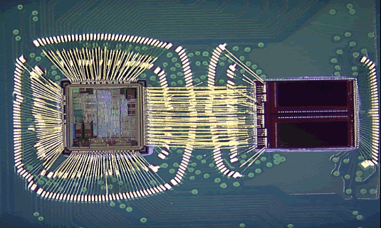
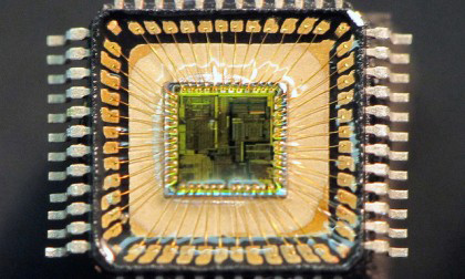
Recover MCU ATmega2560 Flash content and eeprom content, and then make microcontroller atmega2560 cloning after reprogramme the firmware to new MCU, read the firmware from mcu atmega2560 memory;
XTAL1 and XTAL2 are the input and output, respectively, of an inverting amplifier which can be configured for use as an on-chip oscillator, as shown in Figure 1. Either a quartz crystal or ceramic resonator may be used. To drive the device from an external clock source, XTAL2 should be left unconnected while XTAL1 is driven as shown in Figure 2.
There are no requirements on the duty cycle of the external clock signal, since the input to the internal clocking circuitry is through a divide-by-two flip-flop, but minimum and maximum voltage high and low time specifications must be observed if break pic16f631 Mcu .
In idle mode, the CPU puts itself to sleep while all the on-chip peripherals remain active. The mode is invoked by software. The content of the on-chip RAM and all the special functions registers remain unchanged during this mode. The idle mode can be terminated by any enabled interrupt or by a hardware reset. It should be noted that when idle is terminated by a hard ware reset, the device normally resumes program execution, from where it left off, up to two machine cycles before the internal reset algorithm takes control after break microcontroller pic16f628a.
On-chip hardware inhibits access to internal RAM in this event, but access to the port pins is not inhibited. To eliminate the possibility of nated. The only exit from power down is a hardware reset. Reset redefines the SFRs but does not change the on-chip RAM. The reset should not be activated before VCC is restored to its normal operating level and must be held active long enough to allow the oscillator to restart and stabilize.
On the chip are three lock bits which can be left unprogrammed (U) or can be programmed (P) to obtain the additional features listed in the table below:
When lock bit 1 is programmed, the logic level at the EA pin is sampled and latched during reset. If the device is powered up without a reset, the latch initializes to a random value, and holds that value until reset is activated. It is necessary that the latched value of EA be in agreement with the current logic level at that pin in order for the device to function properly before RECOVER MCU.
Recover MCU ATmega1280V Program
Recover MCU ATmega1280V Program from secured eeprom and flash memory, crack microcontroller atmega1280v fuse bit and readout the embedded firmware in the format of heximal from mcu atmega1280v;
1. Non-Recover-While-Write area of flash not functional
Part does not work under 2.4 volts
Incorrect ADC recovering in differential mode
Internal ADC reference has too low value
IN/OUT instructions may be executed twice when Stack is in external RAM
EEPROM recover from application code does not work in Lock Bit Mode 3
Non-Recover-While-Write area of flash not functional if copy microcontroller pic16c771 firmware
The Non-Recover-While-Write area of the flash is not working as expected. The problem is related to the speed of the part when recovering the flash of this area.
Problem Fix/Workaround
– Only use the first 248K of the flash.
– If boot functionality is needed, run the code in the Non-Recover-While-Write area at maximum
1/4th of the maximum frequency of the device at any given voltage. This is done by writing the CLKPR register before entering the boot section of the code
Part does not work under 2.4 volts
The part does not execute code correctly below 2.4 volts
Problem Fix/Workaround
Do not use the part at voltages below 2.4 volts.
Incorrect ADC recovering in differential mode
The ADC has high noise in differential mode. It can give up to 7 LSB error.
Problem Fix/Workaround
Use only the 7 MSB of the result when using the ADC in differential mode after Recover pic16c73b MCU firmware.
Internal ADC reference has too low value
The internal ADC reference has a value lower than specified
Problem Fix/Workaround
– Use AVCC or external reference
– The actual value of the reference can be measured by applying a known voltage to the
ADC when using the internal reference. The result when doing later conversions can then be calibrated.
IN/OUT instructions may be executed twice when Stack is in external RAM
If either an IN or an OUT instruction is executed directly before an interrupt occurs and the stack pointer is located in external ram, the instruction will be executed twice. In some cases this will cause a problem, for example:
– If recovering SREG it will appear that the I-flag is cleared.
– If writing to the PIN registers, the port will toggle twice.
– If recovering registers with interrupt flags, the flags will appear to be cleared.
Problem Fix/Workaround
There are two application work-arounds, where selecting one of them, will be omitting the issue:
– Replace IN and OUT with LD/LDS/LDD and ST/STS/STD instructions
– Use internal RAM for stack pointer.
EEPROM recover from application code does not work in Lock Bit Mode 3 after Recover MCU program.
When the Memory Lock Bits LB2 and LB1 are programmed to mode 3, EEPROM recover does not work from the application code.
Problem Fix/Workaround
Do not set Lock Bit Protection Mode 3 when the application code needs to recover from EEPROM.
Break IC ATmega1280 Eeprom
Break IC ATmega1280 Eeprom and read the firmware from mcu atmega1280 memory, and crack microcontroller atmega1280 security fuse bit by focus ion beam technology;
Port A is an 8-bit bi-directional I/O port with internal pull-up resistors (selected for each bit). The Port A output buffers have symmetrical drive characteristics with both high sink and source capability. As inputs, Port A pins that are externally pulled low will source current if the pull-up resistors are activated.
The Port A pins are tri-stated when a reset condition becomes active, even if the clock is not running. Port B is an 8-bit bi-directional I/O port with internal pull-up resistors (selected for each bit). The Port B output buffers have symmetrical drive characteristics with both high sink and source capability if recover mcu pic18f452 program.
As inputs, Port B pins that are externally pulled low will source current if the pull-up resistors are activated. The Port B pins are tri-stated when a reset condition becomes active, even if the clock is not running.
Port C is an 8-bit bi-directional I/O port with internal pull-up resistors (selected for each bit). The Port C output buffers have symmetrical drive characteristics with both high sink and source capability. As inputs, Port C pins that are externally pulled low will source current if the pull-up resistors are activated. The Port C pins are tri-stated when a reset condition becomes active, even if the clock is not running.
Port D is an 8-bit bi-directional I/O port with internal pull-up resistors (selected for each bit). The Port D output buffers have symmetrical drive characteristics with both high sink and source capability. As inputs, Port D pins that are externally pulled low will source current if the pull-up resistors are activated.
The Port D pins are tri-stated when a reset condition becomes active, even if the clock is not running. Port E is an 8-bit bi-directional I/O port with internal pull-up resistors (selected for each bit). The Port E output buffers have symmetrical drive characteristics with both high sink and source capability.
As inputs, Port E pins that are externally pulled low will source current if the pull-up resistors are activated. The Port E pins are tri-stated when a reset condition becomes active, even if the clock is not running.
Port F serves as analog inputs to the A/D Converter. Port F also serves as an 8-bit bi-directional I/O port, if the A/D Converter is not used. Port pins can provide internal pull-up resistors (selected for each bit). The Port F output buffers have symmetrical drive characteristics with both high sink and source capability after Break IC.
As inputs, Port F pins that are externally pulled low will source current if the pull-up resistors are activated. The Port F pins are tri-stated when a reset condition becomes active, even if the clock is not running. If the JTAG interface is enabled, the pull-up resistors on pins PF7(TDI), PF5(TMS), and PF4(TCK) will be activated even if a reset occurs.
Port G is a 6-bit I/O port with internal pull-up resistors (selected for each bit). The Port G output buffers have symmetrical drive characteristics with both high sink and source capability. As inputs, Port G pins that are externally pulled low will source current if the pull-up resistors are activated. The Port G pins are tri-stated when a reset condition becomes active, even if the clock is not running.
Port H is a 8-bit bi-directional I/O port with internal pull-up resistors (selected for each bit). The Port H output buffers have symmetrical drive characteristics with both high sink and source capability. As inputs, Port H pins that are externally pulled low will source current if the pull-up resistors are activated. The Port H pins are tri-stated when a reset condition becomes active, even if the clock is not running.
Break IC ATmega640V Flash
Break IC ATmega640V and readout the embedded firmware from mcu atmega640v Flash memory and eeprom memory, the protective system of microcontroller atmega640v will be cracked to get access to flash and eeprom memory;
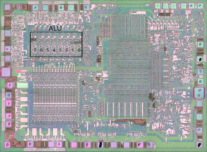
The ATmega640V is a low-power CMOS 8-bit microcontroller based on the AVR enhanced RISC architecture. By executing powerful instructions in a single clock cycle, the ATmega640V achieves throughputs approaching 1 MIPS per MHz allowing the system designer to optimize power consumption versus processing speed.
The AVR core combines a rich instruction set with 32 general purpose working registers. All the 32 registers are directly connected to the Arithmetic Logic Unit (ALU), allowing two independent registers to be accessed in one single instruction executed in one clock cycle.
T5he resulting architecture is more code efficient while achieving throughputs up to ten times faster than conventional CISC microcontrollers before attack microcontroller mc68hc705p6.
The ATmega640V provides the following features: 64K/128K/256K bytes of In-System Programmable Flash with Break-While-Write capabilities, 4K bytes EEPROM, 8K bytes SRAM, 54/86 general purpose I/O lines, 32 general purpose working registers, Real Time Counter (RTC), six flexible Timer/Counters with compare modes and PWM, 4 USARTs, a byte oriented 2-wire Serial Interface, a 16-channel, 10-bit ADC with optional differential input stage with programmable gain, programmable Watchdog Timer with Internal Oscillator, an SPI serial port, IEEE std. 1149.1 compliant JTAG test interface, also used for accessing the On-IC Debug system and programming and six software selectable power saving modes.
The Idle mode stops the CPU while allowing the SRAM, Timer/Counters, SPI port, and interrupt system to continue functioning. The Power-down mode saves the register contents but freezes the Oscillator, disabling all other IC functions until the next interrupt or Hardware Reset when copy pic16lf877 mcu program.
In Power save mode, the asynchronous timer continues to run, allowing the user to maintain a timer base while the rest of the device is sleeping. The ADC Noise Reduction mode stops the CPU and all I/O modules except Asynchronous Timer and ADC, to minimize switching noise during ADC conversions.
In Standby mode, the Crystal/Resonator Oscillator is running while the rest of the device is sleeping. This allows very fast start-up combined with low power consumption. In Extended Standby mode, both the main Oscillator and the Asynchronous Timer continue to run.
The device is manufactured using Atmel’s high-density nonvolatile memory technology. The On-IC ISP Flash allows the program memory to be reprogrammed in-system through an SPI serial interface, by a conventional nonvolatile memory programmer, or by an On-IC Boot program running on the AVR core when Break IC.
The boot program can use any interface to download the application program in the application Flash memory. Software in the Boot Flash section will continue to run while the Application Flash section is updated, providing true Break-While-Write operation.
By combining an 8-bit RISC CPU with In-System Self-Programmable Flash on a monolithic IC, the Atmel ATmega640V is a powerful microcontroller that provides a highly flexible and cost effective solution to many embedded control applications.
The ATmega640V AVR is supported with a full suite of program and system development tools including: C compilers, macro assemblers, program debugger/simulators, in-circuit emulators, and evaluation kits.
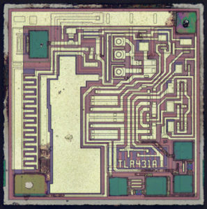
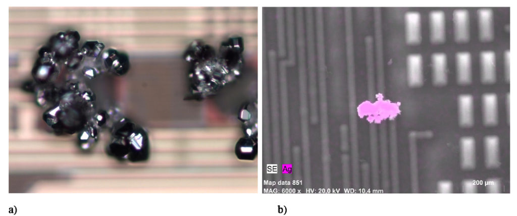
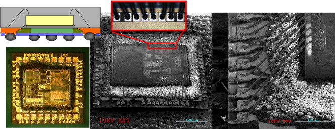
Reverse Engineering Microcontroller ATmega640
Reverse Engineering Microcontroller ATmega640 and readout the embedded content from mcu atmega640, atmega640 mcu protection can be unlocked by focus ion beam;
Features
High Performance, Low Power AVR® 8-Bit Microcontroller
Advanced RISC Architecture
– 135 Powerful Instructions – Most Single Clock Cycle Execution when copy pic18f252 Microcontroller
– 32 x 8 General Purpose Working Registers
– Fully Static Operation
– Up to 16 MIPS Throughput at 16 MHz
– On-Chip 2-cycle Multiplier
High Endurance Non-volatile Memory Segments
– 64K/128K/256K Bytes of In-System Self-Programmable Flash
– 4K Bytes EEPROM
– 8K Bytes Internal SRAM
– Write/Erase Cycles:10,000 Flash/100,000 EEPROM
– Data retention: 20 years at 85°C/ 100 years at 25°C
– Optional Boot Code Section with Independent Lock Bits after recover dspic30f6013a Microcontroller
In-System Programming by On-chip Boot Program
True Reverse engineering-While-Write Operation
– Programming Lock for Software Security
Endurance: Up to 64K Bytes Optional External Memory Space
JTAG (IEEE std. 1149.1 compliant) Interface
– Boundary-scan Capabilities According to the JTAG Standard
– Extensive On-chip Debug Support
– Programming of Flash, EEPROM, Fuses, and Lock Bits through the JTAG Interface
Peripheral Features
– Two 8-bit Timer/Counters with Separate Prescaler and Compare Mode
– Four 16-bit Timer/Counter with Separate Prescaler, Compare- and Capture Mode
– Real Time Counter with Separate Oscillator
– Four 8-bit PWM Channels
– Six/Twelve PWM Channels with Programmable Resolution from 2 to 16 Bits
(ATmega1281/2561, ATmega640/1280/2560)
– Output Compare Modulator
– 8/16-channel, 10-bit ADC (ATmega1281/2561, ATmega640/1280/2560) after Reverse engineering Microcontroller
– Two/Four Programmable Serial USART (ATmega1281/2561,ATmega640/1280/2560)
– Master/Slave SPI Serial Interface
– Byte Oriented 2-wire Serial Interface
– Programmable Watchdog Timer with Separate On-chip Oscillator
– On-chip Analog Comparator
– Interrupt and Wake-up on Pin Change
Special Microcontroller Features
– Power-on Reset and Programmable Brown-out Detection
– Internal Calibrated Oscillator
– External and Internal Interrupt Sources
– Six Sleep Modes: Idle, ADC Noise Reduction, Power-save, Power-down, Standby, and Extended Standby I/O and Packages
– 54/86 Programmable I/O Lines (ATmega1281/2561, ATmega640/1280/2560)
– 64-pad QFN/MLF, 64-lead TQFP (ATmega1281/2561)
– 100-lead TQFP, 100-ball CBGA (ATmega640/1280/2560)
– RoHS/Fully Green
Temperature Range:
– -40°C to 85°C Industrial
Ultra-Low Power Consumption
– Active Mode: 1 MHz, 1.8V: 500 µA
– Power-down Mode: 0.1 µA at 1.8V
Speed Grade:
– ATmega640V/ATmega1280V/ATmega1281V:
0 – 4 MHz @ 1.8 – 5.5V, 0 – 8 MHz @ 2.7 – 5.5V
– ATmega2560V/ATmega2561V:
0 – 2 MHz @ 1.8 – 5.5V, 0 – 8 MHz @ 2.7 – 5.5V
– ATmega640/ATmega1280/ATmega1281:
0 – 8 MHz @ 2.7 – 5.5V, 0 – 16 MHz @ 4.5 – 5.5V
– ATmega2560/ATmega2561:
0 – 16 MHz @ 4.5 – 5.5V
Recover MCU ATtiny861V Flash
Recover MCU ATtiny861V Flash program and eeprom data, crack microcontroller attiny861v protective system and read the firmware out from embedded processor attiny861v memory;
A map of the on-chip memory area called the Special Function Register (SFR) space is shown in Table 1.
Note that not all of the addresses are occupied, and unoccupied addresses may not be implemented on the chip. Recover accesses to these addresses will in general return random data, and write accesses will have an indeterminate effect if attack pic18lf4520 MCU.
User software should not write 1s to these unlisted locations, since they may be used in future products to invoke new features. In that case, the reset or inactive values of the new bits will always be 0.
Timer 2 Registers: Control and status bits are contained in registers T2CON (shown in Table 2) and T2MOD (shown in Table ) for Timer 2. The register pair (RCAP2H, RCAP2L) are the Capture/Reload registers for Timer 2 in 16-bit capture mode or 16-bit auto-reload mode.
Interrupt Registers: The individual interrupt enable bits are in the IE register. Two priorities can be set for each of the six interrupt sources in the IP register.
Table 2. T2CON – Timer/Counter 2 Control Register
MCS-51 devices have a separate address space for Program and Data Memory. Up to 64K bytes each of external Program and Data Memory can be addressed.
If the EA pin is connected to GND, all program fetches are directed to external memory. On the AT89LS52, if EA is connected to VCC, program fetches to addresses 0000H through 1FFFH are directed to internal memory and fetches to addresses 2000H through FFFFH are directed to external memory when copy pic18f458 MCU binary.
The AT89LS52 implements 256 bytes of on-chip RAM. The upper 128 bytes occupy a parallel address space to the Special Function Registers. This means that the upper 128 bytes have the same addresses as the SFR space but are physically separate from SFR space.
When an instruction accesses an internal location above address 7FH, the address mode used in the instruction specifies whether the CPU accesses the upper 128 bytes of RAM or the SFR space. Instructions which use direct addressing access of the SFR space.
For example, the following direct addressing instruction accesses the SFR at location 0A0H (which is P2). MOV 0A0H, #data Instructions that use indirect addressing access the upper 128 bytes of RAM. For example, the following indirect addressing instruction, where R0 contains 0A0H, accesses the data byte at address 0A0H, rather than P2 (whose address is 0A0H) after Recover MCU.
MOV @R0, #data Note that stack operations are examples of indirect addressing, so the upper 128 bytes of data RAM are available as stack space.
Recover MCU ATtiny861 Software
Recover MCU ATtiny861 Software from opened microcontroller attiny861 after crack it, and then read the firmware out from program and eeprom memory of microprocessor attiny861.