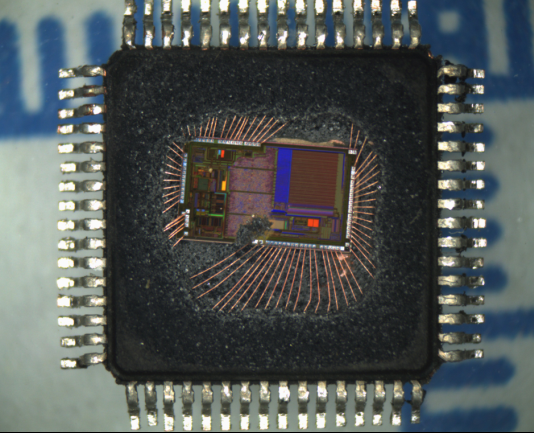
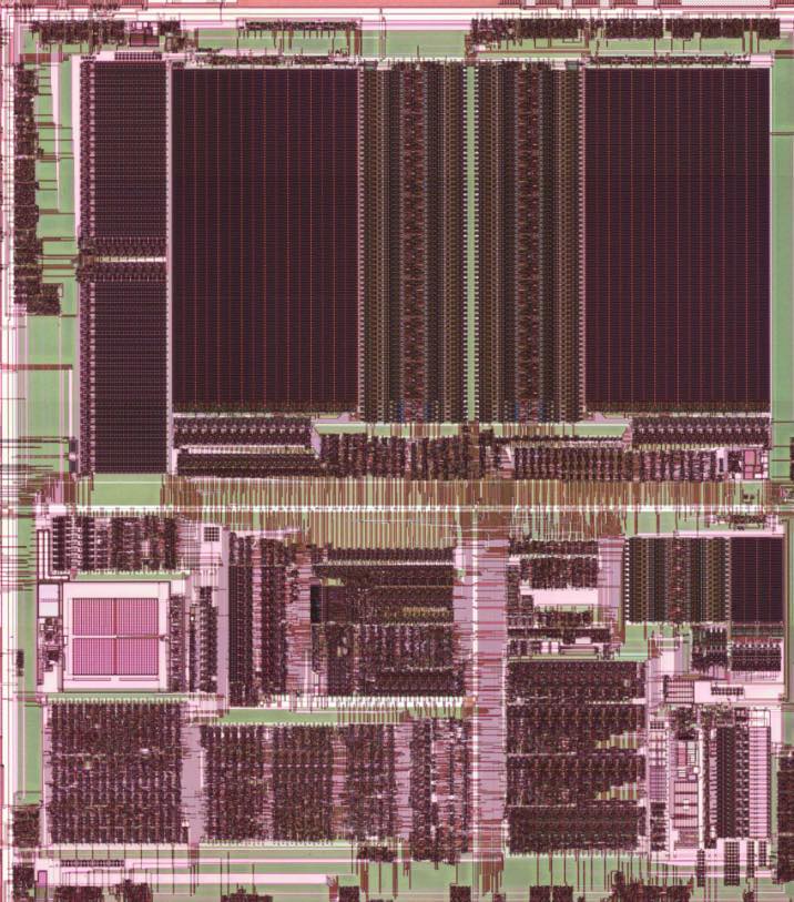
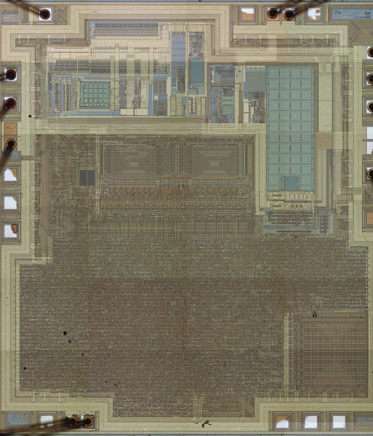
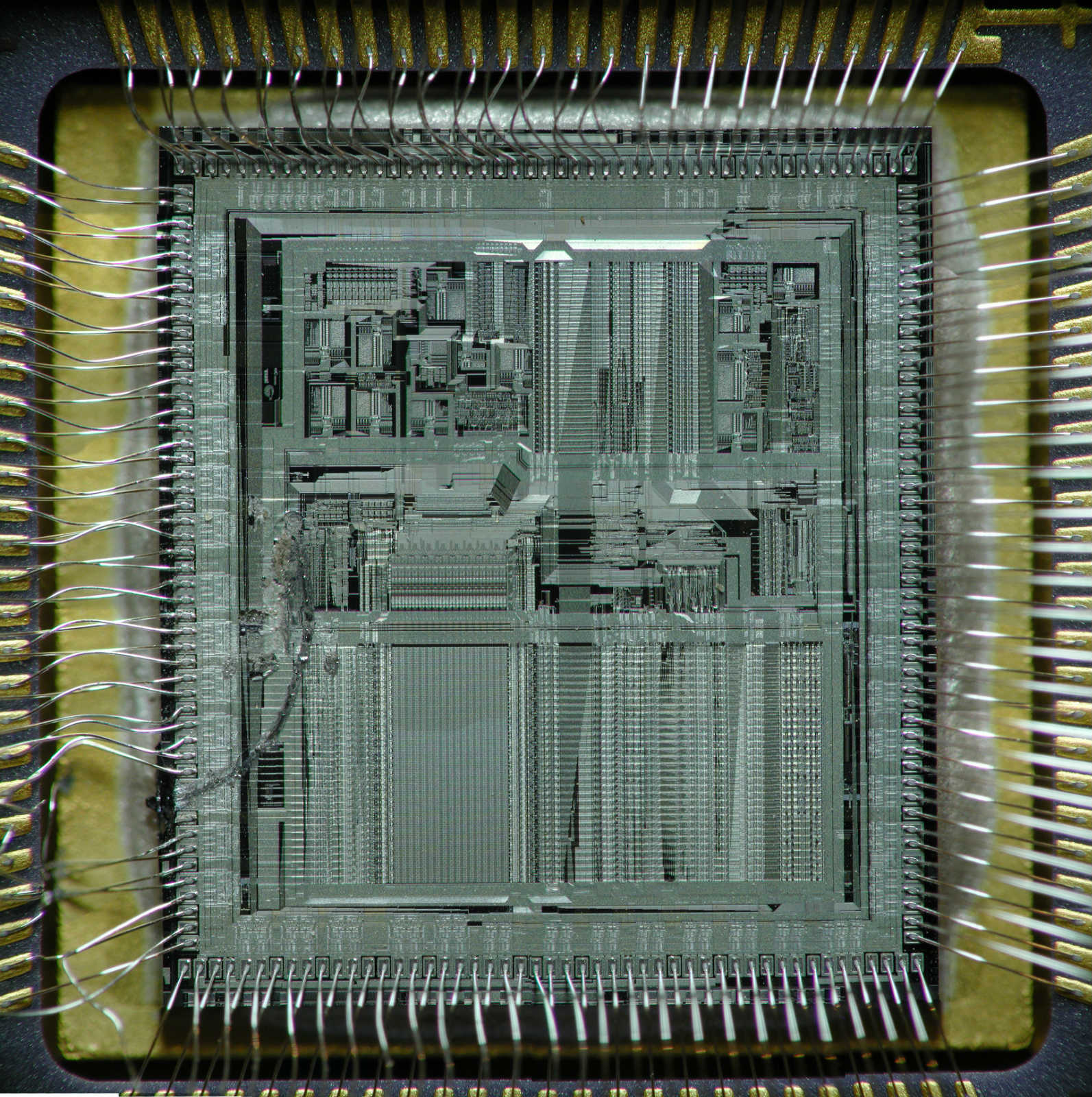
 Break R5F21258SNFP MCU Flash Memory Locking
Break R5F21258SNFP MCU Flash Memory Locking and clone renesas r5f21258sn flash memory content from original chip, extract microprocessor embedded firmware from its flash memory.
R5F21258SNFP has an On-chip Brown-out Detection (BOD) circuit for monitoring the VCC level during operation by comparing it to a fixed trigger level. The trigger level for the BOD can be selected by the fuse BODLEVEL to be
2.7V (BODLEVEL unprogrammed), or 4.0V (BODLEVEL programmed). The trigger level has a hysteresis to ensure spike free Brown-out Detection when copy r5f212aasd locked flash memory data. The hysteresis on the detection level should be interpreted as VBOT+ = VBOT
+ VHYST/2 and VBOT- = VBOT – VHYST/2.
The BOD circuit can be enabled/disabled by the fuse BODEN. When the BOD is enabled (BODEN programmed), and VCC decreases to a value below the trigger level (VBOT- in Figure 11-5), the Brown-out Reset is immediately activated after reverse engineering r5f21226df microprocessor binary code. When VCC increases above the trigger level (VBOT+ in Figure 11-5), the delay counter starts the MCU after the time-out period tTOUT has expired. The BOD circuit will only detect a drop in VCC if the voltage stays below the trigger level for longer than tBOD given in Table 26-3 on page 235.
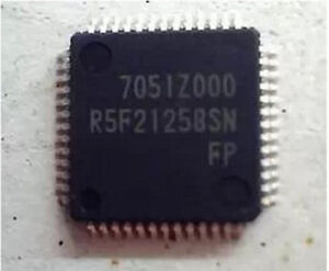
quebrar R5F21258SNFP MCU bloqueio de memória flash e clone renesas r5f21258sn conteúdo de memória flash do chip original, extrair microprocessador firmware incorporado de sua memória flash
R8C R5F21276KFP Microcontroller Reverse Engineering
R8C R5F21276KFP Microcontroller Reverse Engineering will reverse mcu programming sequence and extract protected mcu r5f21276kfp source code from its memory, and then clone firmware to new microcontroller R5F21276JFP;
4 circuits: XIN clock oscillation circuit,
XCIN clock oscillation circuit (32 kHz),
High-speed on-chip oscillator (with frequency adjustment function), Low-speed on-chip oscillator
- Oscillation stop detection: XIN clock oscillation stop detection function
- Frequency divider circuit: Dividing selectable 1, 2, 4, 8, and 16
- Low power consumption modes:
Standard operating mode (high-speed clock, low-speed clock, high-speed on-chip oscillator to break R5F21292SD locked mcu flash memory, low-speed on-chip oscillator), wait mode, stop mode.
8 bits × 1 (with 8-bit prescaler)
Timer mode (period timer), pulse output mode (output level inverted every period), event counter mode, pulse width measurement mode, pulse period measurement mode.
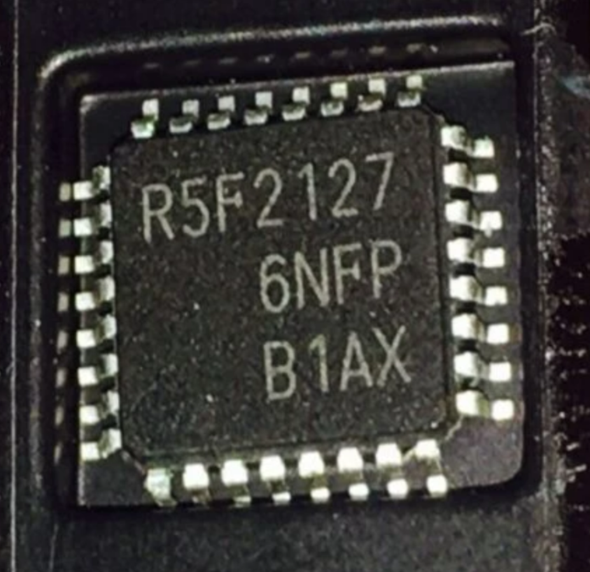
A engenharia reversa do microcontrolador R8C R5F21276KFP reverterá a sequência de programação mcu e extrairá o código-fonte mcu r5f21276kfp protegido de sua memória e, em seguida, clonará o firmware para o novo microcontrolador R5F21276JFP
R0 is a 16-bit register for transfer, arithmetic, and logic operations. The same applies to R1 to R3. R0 can be split into high-order bits (R0H) and low-order bits (R0L) to be used separately as 8-bit data registers to attack renesas r5f21244sd microcontroller protection. R1H and R1L are analogous to R0H and R0L. R2 can be combined with R0 and used as a 32-bit data register (R2R0). R3R1 is analogous to R2R0.
Restore R5F211A2SP IC MCU Flash Memory Data
Restore R5F211A2SP IC MCU Flash Memory Data needs to reverse engineering microcontroller r5f211a2sp locked fuse bit, readout embedded binary file from microprocessor r5f211a2sp flash memory;
The R8C/33A Group of single-chip MCUs incorporates the R8C/Tiny Series CPU core, employing sophisticated instructions for a high level of efficiency. With 1 Mbyte of address space to recover microcontroller r5f21324cnsp flash program, and it is capable of executing instructions at high speed. In addition, the CPU core boasts a multiplier for high-speed operation processing.
Power consumption is low, and the supported operating modes allow additional power control. These MCUs also use an anti-noise configuration to reduce emissions of electromagnetic noise and are designed to withstand EMI.
restaurar R5F211A2SP IC MCU dados de memória flash precisa de engenharia reversa microcontrolador r5f211a2sp bloqueado bit fusível, leitura de arquivo binário incorporado do microprocessador r5f211a2sp memória flash
Integration of many peripheral functions, including multifunction timer and serial interface, reduces the number of system components to break r5f21336tn mcu flash. The R8C/33A Group has data flash (1 KB × 4 blocks) with the background operation (BGO) function.
R8C/Tiny series core
- Number of fundamental instructions: 89
- Minimum instruction execution time:
50 ns (f(XIN) = 20 MHz, VCC = 3.0 to 5.5 V)
100 ns (f(XIN) = 10 MHz, VCC = 2.7 to 5.5 V)
200 ns (f(XIN) = 5 MHz, VCC = 2.2 to 5.5 V)
500 ns (f(XIN) = 2 MHz, VCC = 1.8 to 5.5 V)
- Multiplier: 16 bits × 16 bits ® 32 bits
- Multiply-accumulate instruction: 16 bits × 16 bits + 32 bits ® 32 bits
Operation mode: Single-chip mode (address space: 1 Mbyte)
Break R8C R5F21336TNFP MCU Flash Program
Break R8C R5F21336TNFP MCU Flash Program is a process of cracking renesas microprocessor r5f21336tn flash memory fuse bit, and extract embedded binary file from microcontroller;
There are several issues to consider when trying to minimize the power consumption in an AVR controlled system. In general, sleep modes should be used as much as possible, and the sleep mode should be selected so that as few as possible of the device’s functions are operating.
All functions not needed should be disabled. In particular, the following modules may need special consideration when trying to achieve the lowest possible power consumption in the process of breaking r5f21292sd locked MCU flash memory.
quebrar R8C R5F21336TNFP MCU programa flash é um processo de quebra de microprocessador renesas r5f21336tn memória flash fusível bit, e extrair arquivo binário incorporado do microcontrolador;
If enabled, the ADC will be enabled in all sleep modes. To save power, the ADC should be disabled before entering any sleep mode by attacking renesas r5f21244sd microcontroller protection. When the ADC is turned off and on again, the next conversion will be an extended conversion. Refer to “Analog-to-Digital Converter” on page 189 for details on ADC operation.
When entering Idle mode, the Analog Comparator should be disabled if not used. When entering ADC Noise Reduction mode, the Analog Comparator should be disabled. In the other sleep modes, the Analog Comparator is automatically disabled.
R8C R5F21324CNSP Microcontroller Flash Program Recovery
R8C R5F21324CNSP Microcontroller Flash Program Recovery will help engineer to restore embedded firmware inside flash memory of R5F21324CNSP, fuse bit of microprocessor R5F21324CNSP can be cracked;
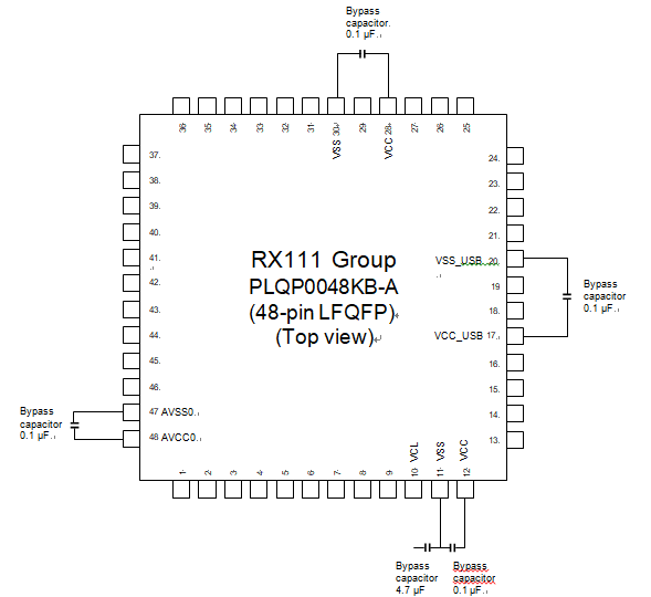
This MCU integrates an internal voltage-down circuit, which is used for lowering the power supply voltage in the internal MCU to adjust automatically to the optimum level. A 4.7-μF capacitor needs to be connected between this internal voltage-down power supply (VCL pin) and VSS pin.
R8C R5F21324CNSP microcontrolador de recuperação do programa flash ajudará o engenheiro a restaurar o firmware incorporado dentro da memória flash de R5F21324CNSP, bit de fusível do microprocessador R5F21324CNSP pode ser rachado;
Below Figure 1 to Figure 5.64 shows how to connect external capacitors. Place an external capacitor close to the pins especially when dumping renesas r5f212a7 protected MCU flash program. Do not apply the power supply voltage to the VCL pin. Insert a multilayer ceramic capacitor as a bypass capacitor between each pair of the power supply pins. Implement a bypass capacitor to the MCU power supply pins as close as possible.
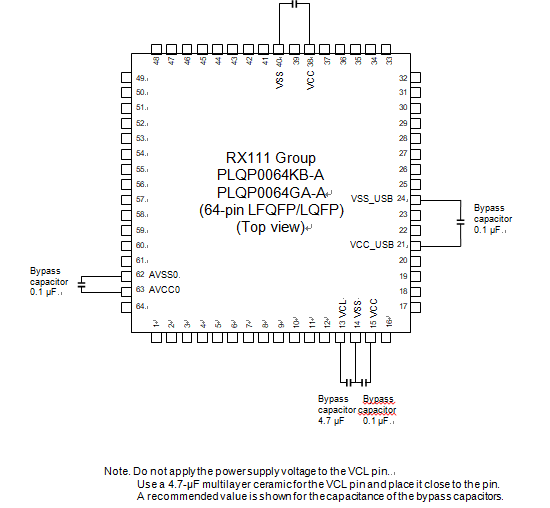
Use a 4.7-µF multilayer ceramic for the VCL pin and place it close to the pin. A recommended value is shown for the capacitance of the bypass capacitors
Use a recommended value of 0.1 μF as the capacitance of the capacitors. For the capacitors related to crystal oscillation, see section 9, Clock Generation Circuit in the User’s Manual: Hardware. For the capacitors related to analog modules, also see section 30, 12-Bit A/D Converter (S12ADb) in the User’s Manual: Hardware.
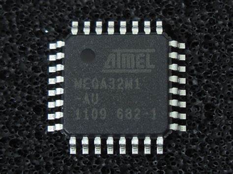
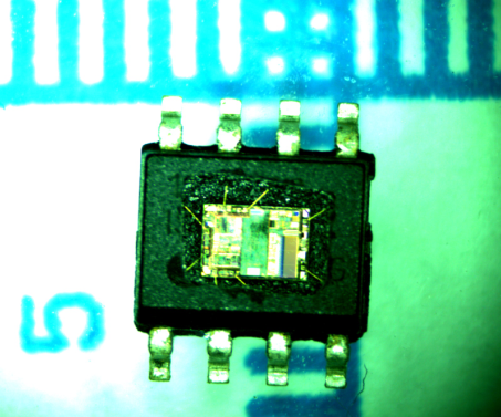
Locked MCU ATMEGA32M1 Firmware Recovery
Locked MCU ATMEGA32M1 Firmware Recovery needs to unlock atmega32m1 microcontroller flash memory, then readout embedded software from atmega32m1 processor;
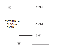
To drive the device from an external clock source, XTAL1 should be driven as shown in below Figure. To run the device on an external clock, the CKSEL Fuses must be programmed to “0000”. By programming the CKOPT Fuse, the user can enable an internal 36 pF capacitor between XTAL1 and GND, and XTAL2 and GND.
When applying an external clock, it is required to avoid sudden changes in the applied clock frequency to ensure stable operation of the MCU. A variation in frequency of more than 2% from one clock cycle to the next can lead to unpredictable behavior in the process of breaking atmega16l locked mcu flash memory. It is required to ensure that the MCU is kept in Reset during such changes in the clock frequency.
a recuperação de firmware MCU ATMEGA32M1 bloqueada precisa desbloquear a memória flash do microcontrolador atmega32m1 e, em seguida, ler o software incorporado do processador atmega32m1;
For AVR microcontrollers with Timer/Counter Oscillator pins (TOSC1 and TOSC2), the crystal is connected directly between the pins. By programming the CKOPT Fuse, the user can enable internal capacitors on XTAL1 and XTAL2 to recover microprocessor atmega16 protective flash, thereby removing the need for external capacitors. The Oscillator is optimized for use with a 32.768 kHz watch crystal. Applying an external clock source to TOSC1 is not recommended.
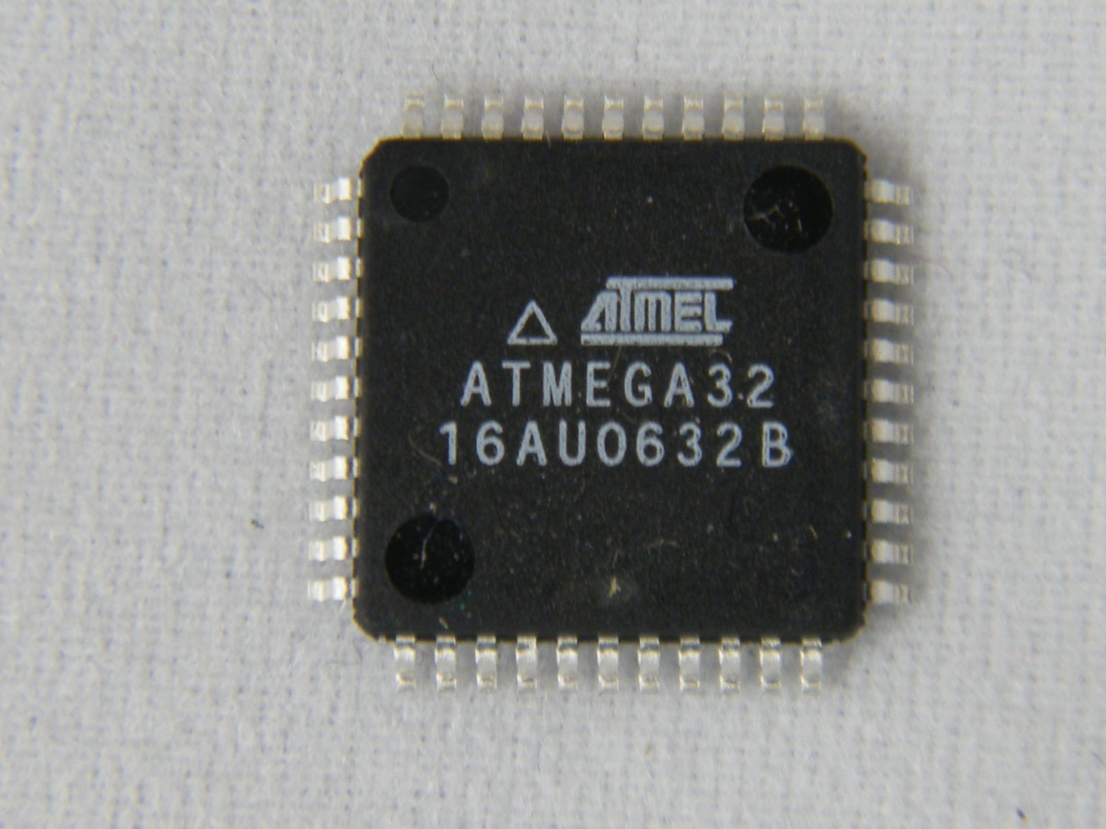
Breaking Encrypted ATMEGA32A MCU Flash
Breaking Encrypted ATMEGA32A MCU Flash and pull microcontroller atmega32a firmware out from its flash and eeprom memory, the software file of atmega32a atmel chip can be readout directly by programmer after reset the fuse bit;
EEPROM data corruption can easily be avoided by following this design recommendation: Keep the AVR RESET active (low) during periods of insufficient power supply voltage. This can be done by enabling the internal Brown-out Detector (BOD).
If the detection level of the internal BOD does not match the needed detection level, an external low VCC Reset Protection circuit can be used. If a reset occurs while a write operation is in progress of breaking atmega16l locked mcu flash memory, the write operation will be completed provided that the power supply voltage is sufficient.
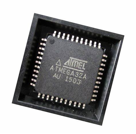
quebrando o flash criptografado ATMEGA32A MCU e puxar o microcontrolador atmega32a firmware para fora de sua memória flash e eeprom, o arquivo de software do chip atmega32a atmel pode ser lido diretamente pelo programador após a redefinição do bit de fusível;
Below Figure presents the principal clock systems in the AVR and their distribution. All of the clocks need not be active at a given time. In order to reduce power consumption, the clocks to modules not being used can be halted by using different sleep modes, as described in “Power Management and Sleep Modes” on page 39. The clock systems are detailed below Figure.
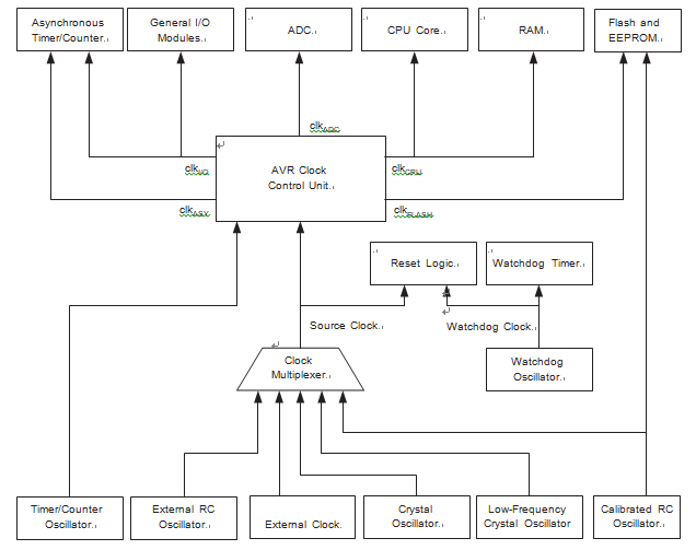
The CPU clock is routed to parts of the system concerned with operation of the AVR core. Examples of such mod- ules are the General Purpose Register File by recover atmega16 microprocessor firmware, the Status Register and the Data memory holding the Stack Pointer. Halting the CPU clock inhibits the core from performing general operations and calculations.
Restoring ATmega32L Microprocessor Memory Software
Restoring ATmega32L Microprocessor Memory Software in the format of heximal or binary, original memory data inside atmega32l mcu will be cloned and embedded firmware will be readout from atmega32l;
The EEPROM Write Enable Signal EEWE is the write strobe to the EEPROM. When address and data are correctly set up, the EEWE bit must be written to one to write the value into the EEPROM. The EEMWE bit must be written to one before a logical one is written to EEWE, otherwise no EEPROM write takes place. The following pro- cedure should be followed when writing the EEPROM (the order of steps 3 and 4 is not essential):
- Wait until EEWE becomes zero.
- Wait until SPMEN in SPMCR becomes zero.
- Write new EEPROM address to EEAR (optional).
- Write new EEPROM data to EEDR (optional).
- Write a logical one to the EEMWE bit while writing a zero to EEWE in EECR.
- Within four clock cycles after setting EEMWE, write a logical one to EEWE.
The EEPROM can not be programmed during a CPU write to the Flash memory. The software must check that the Flash programming is completed before initiating a new EEPROM write to reverse engineer atmega8a microchip memory. Step 2 is only relevant if the software con- tains a boot loader allowing the CPU to program the Flash.
If the Flash is never being updated by the CPU, step 2 can be omitted. See “Boot Loader Support – Read-While-Write Self-Programming” on page 201 for details about boot programming.
Caution: An interrupt between step 5 and step 6 will make the write cycle fail, since the EEPROM Master Write Enable will time-out. If an interrupt routine accessing the EEPROM is interrupting another EEPROM access.
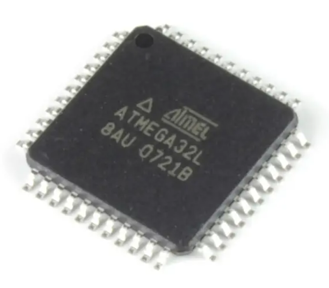
restaurando o software de memória do microprocessador ATmega32L no formato de heximal ou binário, os dados de memória originais dentro do atmega32l mcu serão clonados e o firmware incorporado será lido a partir do atmega32
the EEAR or EEDR Register will be modified, causing the interrupted EEPROM access to fail. It is recommended to have the Global Interrupt Flag cleared during all the steps to avoid these problems.
When the write access time has elapsed, the EEWE bit is cleared by hardware in order to restore microcontroller atmega8l flash data. The user software can poll this bit and wait for a zero before writing the next byte. When EEWE has been set, the CPU is halted for two cycles before the next instruction is executed.
Protected ATmega32 MCU Eeprom Recovery
Protected ATmega32 MCU Eeprom Recovery starts from crack atmega32 microcontroller security fuse bit, and then extract source code from atmega32 mcu flash and eeprom memory;
These bits are reserved bits in the ATmega32 and will always read as zero.
The EEPROM Address Registers – EEARH and EEARL – specify the EEPROM address in the 512 bytes EEPROM space. The EEPROM data bytes are addressed linearly between 0 and 511 by pulling atmega8 mcu flash content out from its memory. The initial value of EEAR is undefined. A proper value must be written before the EEPROM may be accessed.
For the EEPROM write operation, the EEDR Register contains the data to be written to the EEPROM in the address given by the EEAR Register. For the EEPROM read operation, the EEDR contains the data read out from the EEPROM at the address given by EEAR.
Writing EERIE to one enables the EEPROM Ready Interrupt if the I bit in SREG is set. Writing EERIE to zero disables the interrupt by restoring microcontroller atmega8l flash data. The EEPROM Ready interrupt generates a constant interrupt when EEWE is cleared.
protegido ATmega32 MCU eeprom recuperação começa a partir de crack atmega32 microcontrolador de segurança fusível bit e, em seguida, extrair o código-fonte do atmega32 mcu flash e memória eeprom
The EEMWE bit determines whether setting EEWE to one causes the EEPROM to be written. When EEMWE is set, setting EEWE within four clock cycles will write data to the EEPROM at the selected address If EEMWE is zero, setting EEWE will have no effect.
When EEMWE has been written to one by software, hardware clears the bit to zero after four clock cycles. See the description of the EEWE bit for an EEPROM write procedure.
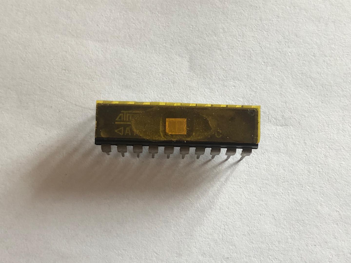
Break ATmega16L Locked MCU Flash Memory
Break ATmega16L Locked MCU Flash Memory and copy heximal code to new atmega16l microprocessor, after extract embedded firmware from microcontroller atmega16l;
The Microchip AVR® ATmega8A contains 512 bytes of data EEPROM memory. It is organized as a separate data space, in which single bytes can be read and written.
The EEPROM has an endurance of at least 100,000 write/erase cycles. The access between the EEPROM and the CPU is described bellow, specifying the EEPROM Address Registers when crack atmega16a microcontroller flash memory, the EEPROM Data Register, and the EEPROM Control Register.
The EEPROM Access Registers are accessible in the I/O space.
The write access time for the EEPROM is given in Table 8-1 on page 27. A self-timing function, however, lets the user software detect when the next byte can be written.
quebrar ATmega16L bloqueado MCU memória flash e copiar código heximal para o novo microprocessador atmega16l, após extrair firmware incorporado do microcontrolador atmega16l
If the user code contains instructions that write the EEPROM, some precautions must be taken in order to recover atmega16 microprocessor firmware. In heavily filtered power supplies, VCC is likely to rise or fall slowly on
Power-up/down. This causes the device for some period of time to run at a voltage lower than specified as mini- mum for the clock frequency used.