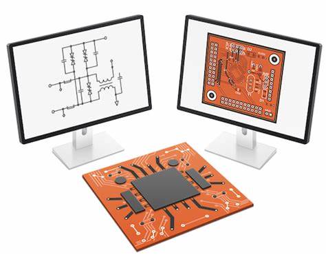
 PCB Development Accurary
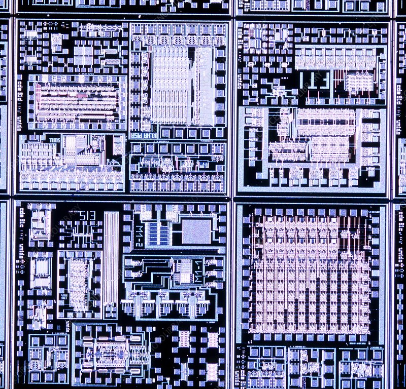
Refers to the PCB Development Accurary, depends on two aspects, one is the accuracy of the software, one for the original image accuracy. Those companies who provide circuit board development service in the current market possess broad variety of precision technical capacity, and some of them have lower accuracy of PCB reverse engineering as a result of absence of high technical ability, but some of them can reach 1mil accuracy of PCB card cloning.
There is no restriction on precision if the software apply 32-bit floating point, so the most important thing depends on the accuracy of the original scanned image, for example, if with 100 million pixels, the picture can be washed 5-inch photos, but if we want it to wash into a 20-inch photos, it simply can not see, so for a high precision circuit board is, Choosing a higher DPI is necessary and critical when scaning the printed circuit board which will help to obtain an good solution pictures.
The definition of DPI is quantity of points per inch. It simply stand for the distance between two points of the scanned image is 1mil, so if DPI is 400, then the distance between two points on the image is 1000/400 = 2.5 mil, that means the accuracy is 2.5mil.
This is the most scientific measurement way, although some people claim the accurary can below 1mil, it is a prerequisite. In fact, the pcb development accurary largely depends on the original image accuracy.
To sum up, DPI value setting on the scaning machine should be determined by the requirement level of accurary of PCB board which is ready to be developped, for instance, line spacing of mobile phone circuit board usually below 1mil, then the value of DPI need to be set at more than 1000 . Scanner on the market today can satisfy this condition.
But it is hard to say the higher DPI being set, the better PCB circuitry pattern scanning job can be done.
Since higher DPI is too large to install and process in the hardware enviroment which has much higher requirement on the hardware, so the specific settings of DPI value should be adjustable according to specific pwb and their corresponding requirement. For the PCB board schematic diagram restoration with general accuracy requirement need to generally use 400DPI is enough.
PCB Repair for 3 different kinds of Circuits
1 Power Supply Circuit:
During the circuit board repair process, power supply part should be inspected at the first hand and then come to the other part. +/-5V,
Power supply failure can occur under below several situation:
(1) NO power supply voltage or power supply voltage is deficiency, NC system is often used +/-5V, +/-12V, +/-15V and +/-24V, a few of them use +3.3V, and the varied or unstable voltage of power supply will cause the system working impropery;
(2) Use voltmeter to test the voltage of power supply, and the result show is normal. Voltage waveform detected by oscillograph has shown the existence of big ripple. This situation maybe caused by open circuit of Filtering capacitance, bad rectifier diode or cold soldering, but sometimes it could be caused by an overloaded component which has been brokendown and damaged by power.
(3) System can run properly when it is just being opened, after a while of operating, the voltage begin to drop off. This is usually caused by voltage stabilizing circuit and large power triode.
(4) The voltage decrease accompany with temperature increase maybe cause by component cold soldering, it is electrical connection can be affected negatively when the temperature high up.
(5) NO power supply voltage or supply voltage decreases significantly will cause the system to interrupt or stop working, this fault can be detected and spotted easier.
(6) When the capacity of power supply load drop off or filter circuit become invalid, it will cause the system halt suddenly, this situation which is very difficult to justify can bring damage to the equipment and facility even get personnel wound.
2 Clock Circuit:
Clock circuit mainly exist on the systematic motherboard, it is the foundation of large-scale integrated circuit system through which it can work, it can generate the constant square signal in the circuit base upon the crystal oscillator (commonly known as crystal), Once the crystal oscillator stop working, it is same as the heart of human being stop beating, the whole system will fall into the status of paralyzed, only after crystal can work under normal condition, the systematic circuit can operate under the command of CPU according to the frequency of crystal. The number and frequency of the crystal could be different due to the variety of numerical control system, but generally will at least one crystal, different clock frequencies required by the other circuit can be solved by frequency dividing circuit or other crystal. Crystal possess a higher rate of failure or damage, below are some malfuntions of crystal:
(1) Leakage: Use multimeter and switch to P*10K level to test it, if the resistance is infinite, then it can be viewed as normal;
(2) Internal OPEN CIRCUIT: Value of resistance is infinite tested by Use multimeter, can fail to generate oscillating pulse in the circuit;
(3) Alternative crystal: Due to the transformation of crytal will cause its internal parameter change which can only be detected by osillagraph or cymometer. Although the crystal can still has oscillation, but the clock frequency is deviated from its nominal value, and the still existing oscillation pulse can’t make system circuit work properly due to the value of oscillation is wrong. Only cymometer can test its tolerance now.
(4) In clock circuit, the both ends of crystal would be connected to ground by one ceramic capacitor value range from several picofarads to tens picofarads, failure of the clock circuit result from this capacitor leakage, deterioration is also more common.
The best tool to test whether the crystal is good or bad could be oscillagraph or cymometer, multimeter is very difficult to detect the root cause.
3 Reset Circuit
Reset circuit also exist in the circuit system of motherboard, it is unique set of large-scale digital integrated circuit. Microprocessor and interface circuit are all possess reset terminal. Reset pulse generate by reset circuit will clear the progam counter, force CPU recall the orginal files from the memory, execute initiation process on all the controller chips, system will occurs the phenomenon of disorder or crash as a result of faulty reset circuit, the method of using cymometer to illustrate the reset pulse is turn on/off power supply repeatly, observe and record the pulse value at the right moment of power supply on/off since it should be the normal square wave-form. If there is no existence of reset pulse, all the resistor, capacitor and transistor in the reset circuit should be detected. The reset terminal of integrated circuit should be regular low or high electrical level, or else, it is probably the malfunctional reset circuit or damaged integrated circuit.
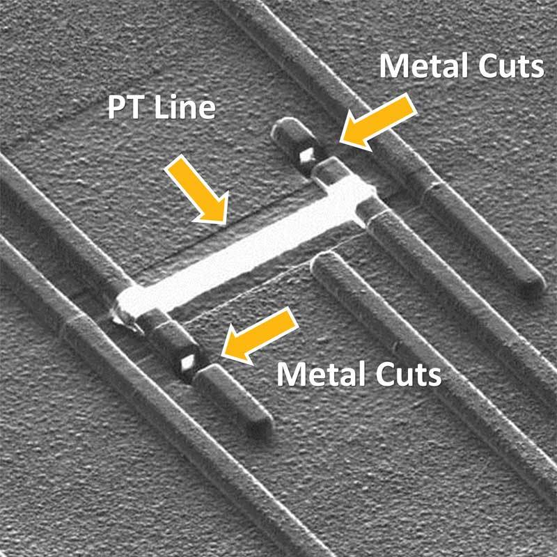
Reverse Engineering IC ATmega1284PV Firmware
Reverse Engineering IC ATmega1284PV structure to locate the security fuse bit, by unlocking MCU ATmega1284 memory and readout ATmega1284 IC Firmware.
Timer/Counter0 is a general purpose 8-bit Timer/Counter module, with two independent Output Compare Units, and with PWM support. It allows accurate program execution timing (event management) and wave generation. The main features are:
Two Independent Output Compare Units
Double Buffered Output Compare Registers
Clear Timer on Compare Match (Auto Reload)
Glitch Free, Phase Correct Pulse Width Modulator (PWM)
Variable PWM Period
Frequency Generator
Three Independent Interrupt Sources (TOV0, OCF0A, and OCF0B)
A simplified block diagram of the 8-bit Timer/Counter is shown in Figure 38. For the actual placement of I/O pins, refer to “Pinout ATmega640/1280/2560” on page 2. CPU accessible I/O Registers, including I/O bits and I/O pins, are shown in bold. The device-specific I/O Register and bit locations are listed in the “8-bit Timer/Counter Register Description” on page 128.
The Timer/Counter (TCNT0) and Output Compare Registers (OCR0A and OCR0B) are 8-bit registers. Interrupt request (abbreviated to Int.Req. in the figure) signals are all visible in the Timer Interrupt Flag Register (TIFR0). All interrupts are individually masked with the Timer Interrupt Mask Register (TIMSK0). TIFR0 and TIMSK0 are not shown in the figure.
The Timer/Counter can be clocked internally, via the prescaler, or by an external clock source on the T0 pin. The Clock Select logic block controls which clock source and edge the Timer/Counter uses to increment (or decrement) its value when attack mcu pic16c558 program.
The Timer/Counter is inactive when no clock source is selected. The output from the Clock Select logic is referred to as the timer clock (clkT0).
The double buffered Output Compare Registers (OCR0A and OCR0B) are compared with the Timer/Counter value at all times. The result of the compare can be used by the Waveform Generator to generate a PWM or variable frequency output on the Output Compare pins (OC0A and OC0B). See “Output Compare Unit” on page 119. for details.
The Compare Match event will also set the Compare Flag (OCF0A or OCF0B) which can be used to generate an Output Compare interrupt request.
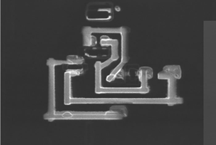
Break MCU ATmega128PA Heximal
Break MCU ATmega128APA flash memory and readout chip ATmega128PA content inside it in the format of Heximal, the code can be reprogrammed to new ATmega128PA microcontroller for cloning;
OC1A/PCINT5, Bit 5
OC1A, Output Compare Match A output: The PB5 pin can serve as an external output for the Timer/Counter1 Output Compare A. The pin has to be configured as an output (DDB5 set (one)) to serve this function. The OC1A pin is also the output pin for the PWM mode timer function.
PCINT5, Pin Change Interrupt source 5: The PB7 pin can serve as an external interrupt source.
OC2A/PCINT4, Bit 4
OC2A, Output Compare Match output: The PB4 pin can serve as an external output for the Timer/Counter2 Output Compare. The pin has to be configured as an output (DDB4 set (one)) to serve this function. The OC2A pin is also the output pin for the PWM mode timer function when recover mcu pic16c554 software.
PCINT4, Pin Change Interrupt source 4: The PB7 pin can serve as an external interrupt source.
MISO/PCINT3 – Port B, Bit 3
MISO: Master Data input, Slave Data output pin for SPI channel. When the SPI is enabled as a master, this pin is configured as an input regardless of the setting of DDB3. When the SPI is enabled as a slave, the data direction of this pin is controlled by DDB3. When the pin is forced to be an input, the pull-up can still be controlled by the PORTB3 bit.
PCINT3, Pin Change Interrupt source 3: The PB7 pin can serve as an external interrupt source when Break MCU heximal.
MOSI/PCINT2 – Port B, Bit 2
MOSI: SPI Master Data output, Slave Data input for SPI channel. When the SPI is enabled as a slave, this pin is configured as an input regardless of the setting of DDB2. When the SPI is enabled as a master, the data direction of this pin is controlled by DDB2. When the pin is forced to be an input, the pull-up can still be controlled by the PORTB2 bit.
PCINT2, Pin Change Interrupt source 2: The PB7 pin can serve as an external interrupt source.
SCK/PCINT1 – Port B, Bit 1
SCK: Master Clock output, Slave Clock input pin for SPI channel. When the SPI is enabled as a slave, this pin is configured as an input regardless of the setting of DDB1. When the SPI0 is enabled as a master, the data direction of this pin is controlled by DDB1. When the pin is forced to be an input, the pull-up can still be controlled by the PORTB1 bit.
PCINT1, Pin Change Interrupt source 1: The PB7 pin can serve as an external interrupt source.
Reverse Engineering MCU Chip ATmega1284P Flash
Reverse Engineering MCU Chip ATmega1284P which is executed in the reverse order of microcontroller manufacturing, read Flash code from microcontroller ATmega1284P memory, and make ATmega1284P MCU cloning;

Most port pins have alternate functions in addition to being general digital I/Os. Figure 37 shows how the port pin control signals from the simplified Figure 34 can be overridden by alternate functions.
The overriding signals may not be present in all port pins, but the figure serves as a generic description applicable to all port pins in the AVR mcu chip family.
When this bit is written to one, the pull-ups in the I/O ports are disabled even if the DDxn and PORTxn Registers are configured to enable the pull-ups ({DDxn, PORTxn} = 0b01) if attack mcu attiny2313 firmware.
See “Configuring the Pin” on page 82 for more details about this feature. OC0A, Output Compare Match A output: The PB7 pin can serve as an external output for the Timer/Counter0 Output Compare.
The pin has to be configured as an output (DDB7 set “one”) to serve this function. The OC0A pin is also the output pin for the PWM mode timer function.
OC1C, Output Compare Match C output: The PB7 pin can serve as an external output for the Timer/Counter1 Output Compare C.
The pin has to be configured as an output (DDB7 set (one)) to serve this function. The OC1C pin is also the output pin for the PWM mode timer function.
PCINT7, Pin Change Interrupt source 7: The PB7 pin can serve as an external interrupt source. OC1B, Output Compare Match B output: The PB6 pin can serve as an external output for the Timer/Counter1 Output Compare B. The pin has to be configured as an output (DDB6 set (one)) to serve this function.
The OC1B pin is also the output pin for the PWM mode timer function when Reverse engineering Mcu chip. PCINT6, Pin Change Interrupt source 6: The PB7 pin can serve as an external interrupt source.
Break Mcu ATmega644PV Code
Break MCU ATmega644PV and clone heximal code from Microcontroller ATmega644PV, the code can be extracted from ATmega644PV chip program memory;
The External Interrupts are triggered by the INT7:0 pin or any of the PCINT23..0 pins. Observe that, if enabled, the interrupts will trigger even if the INT7:0 or PCINT23..0 pins are configured as outputs. This feature provides a way of generating a software interrupt.
The Pin change interrupt PCI2 will trigger if any enabled PCINT23:16 pin toggles, Pin change interrupt PCI1 if any enabled PCINT15:8 toggles and Pin change interrupts PCI0 will trigger if any enabled PCINT7..0 pin toggles. PCMSK2, PCMSK1 and PCMSK0 Registers control which pins contribute to the pin change interrupts if copy Mcu pic16c554a eeprom.
Pin change interrupts on PCINT23 ..0 are detected asynchronously. This implies that these interrupts can be used for waking the part also from sleep modes other than Idle mode.
The External Interrupts can be triggered by a falling or rising edge or a low level. This is set up as indicated in the specification for the External Interrupt Control Registers – EICRA (INT3:0) and EICRB (INT7:4). When the external interrupt is enabled and is configured as level triggered, the interrupt will trigger as long as the pin is held low if copy microcontroller pic16c76 heximal.
Note that recognition of falling or rising edge interrupts on INT7:4 requires the presence of an I/O clock, described in “Clock Systems and their Distribution” on page 39. Low level interrupts and the edge interrupt on INT3:0 are detected asynchronously.
This implies that these interrupts can be used for waking the part also from sleep modes other than Idle mode. The I/O clock is halted in all sleep modes except Idle mode.
Note that if a level triggered interrupt is used for wake-up from Power-down, the required level must be held long enough for the MCU to complete the wake-up to trigger the level interrupt when recover chip epm7064aetc100 software.
If the level disappears before the end of the Start-up Time, the MCU will still wake up, but no interrupt will be generated. The start-up time is defined by the SUT and CKSEL Fuses as described in “System Clock and Clock Options” on page 39.
The External Interrupts 3 – 0 are activated by the external pins INT3:0 if the SREG I-flag and the corresponding interrupt mask in the EIMSK is set. The level and edges on the external pins that activate the interrupts are defined in Table 31.
Edges on INT3..INT0 are registered asynchronously. Pulses on INT3:0 pins wider than the minimum pulse width given in Table 32 will generate an interrupt. Shorter pulses are not guaranteed to generate an interrupt. If low level interrupt is selected, the low level must be held until the completion of the currently executing instruction to generate an interrupt.
If enabled, a level triggered interrupt will generate an interrupt request as long as the pin is held low. When changing the ISCn bit, an interrupt can occur. Therefore, it is recommended to first disable INTn by clearing its Interrupt Enable bit in the EIMSK Register.
Then, the ISCn bit can be changed. Finally, the INTn interrupt flag should be cleared by writing a logical one to its Interrupt Flag bit (INTFn) in the EIFR Register before the interrupt is reenabled.
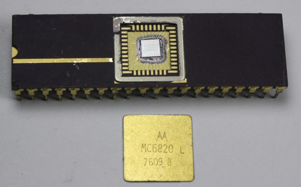
Recover Microcontroller ATmega644P Flash
Recover Microcontroller ATmega644P Flash memory content is a process to extract ATmega644p MCU memory heximal by crack processor’s fuse bit;

To further ensure program security, alterations to the Watchdog set-up must follow timed sequences. The sequence for clearing WDE and changing time-out configuration is as follows:
(WDCE) and WDE. A logic one must be written to WDE regardless of the previous value of the WDE bit. (WDP) as desired, but with the WDCE bit cleared. This must be done in one operation.
The following code example shows one assembly and one C function for turning off the Watchdog Timer. The example assumes that interrupts are controlled (e.g. by disabling interrupts globally) so that no interrupts will occur during the execution of these functions if break Microcontroller pic16f628a content.
Note: If the Watchdog is accidentally enabled, for example by a runaway pointer or brown-out condition, the device will be reset and the Watchdog Timer will stay enabled. If the code is not set up to handle the Watchdog, this might lead to an eternal loop of time-out resets.
To avoid this situation, the application software should always clear the Watchdog System Reset Flag (WDRF) and the WDE control bit in the initialisation routine, even if the Watchdog is not in use. In the same operation, write a logic one to the Watchdog change enable bit to attack pic12f510 program.
Break IC PIC18F4620 Program
Break IC PIC18F4620 security fuse bit and read PIC18F4620 program from flash memory, then copy eeprom content from protected microchip PIC18F4620 processor;
Possible Hardware fuse Watchdog always on (WDTON) for fail-safe modeThe Watchdog Timer (WDT) is a timer counting cycles of a separate on-chip 128 kHz oscillator.
The WDT gives an interrupt or a system reset when the counter reaches a given time-out value. In normal operation mode, it is required that the system uses the WDR – Watchdog Timer Reset – instruction to restart the counter before the time-out value is reached if copy mcu xc18v04pc44c program.
If the system doesn’t restart the counter, an interrupt or system reset will be issued.
In Interrupt mode, the WDT gives an interrupt when the timer expires. This interrupt can be used to wake the device from sleep-modes, and also as a general system timer.
One example is to limit the maximum time allowed for certain operations, giving an interrupt when the operation has run longer than expected after copy chip pic16f73 program.
Within the next four clock cycles, write the WDE and Watchdog prescaler bitsIn System Reset mode, the WDT gives a reset when the timer expires.
This is typically used to prevent system hang-up in case of runaway code. The third mode, Interrupt and System Reset mode, combines the other two modes by first giving an interrupt and then switch to System Reset mode when recover mcu pic16c63a software.
This mode will for instance allow a safe shutdown by saving critical parameters before a system reset. The Watchdog always on (WDTON) fuse, if programmed, will force the Watchdog Timer to System Reset mode.
With the fuse programmed the System Reset mode bit (WDE) and Interrupt mode bit (WDIE) are locked to 1 and 0 respectively.
Recover MCU ATmega644PA Flash
Recover MCU ATmega644PA Flash memory content after crack microcontroller ATmega644PA protection and extract code from microprocessor ATmega644PA memory.
When the BOD is enabled, and VCC decreases to a value below the trigger level (VBOT- in Figure 29), the Brown-out Reset is immediately activated. When VCC increases above the trigger level (VBOT+ in Figure 29), the delay counter starts the MCU after the Time- out period tTOUT has expired if recover mcu pic18f452 program.
The BOD circuit will only detect a drop in VCC if the voltage stays below the trigger level for longer than tBOD given in Table 23. When the Watchdog times out, it will generate a short reset pulse of one CK cycle duration.
On the falling edge of this pulse, the delay timer starts counting the Time-out period tTOUT. See “Watchdog Timer” on page 56. for details on operation of the Watchdog Timer after break chip pic12cr509a flash.
ATmega644PA features an internal bandgap reference. This reference is used for Brown-out Detection, and it can be used as an input to the Analog Comparator or the ADC.
The voltage reference has a start-up time that may influence the way it should be used. The start-up time is given in Table 26. To save power, the reference is not always turned The reference is on during the following situations if attack dsp mcu tms320f241pg heximal:
When the BOD is enabled (by programming the BODLEVEL [2..0] Fuse).
When the bandgap reference is connected to the Analog Comparator (by setting the ACBG bit in ACSR) before recover mcu flash. When the ADC is enabled.
Thus, when the BOD is not enabled, after setting the ACBG bit or enabling the ADC, the user must always allow the reference to start up before the output from the Analog Comparator or ADC is used.
To reduce power consumption in Power-down mode, the user can avoid the three conditions above to ensure that the reference is turned off before entering Power-down mode when recover mcu flash. ATmega644PA has an Enhanced Watchdog Timer (WDT). The main features are:
Clocked from separate On-chip Oscillator
3 Operating modes
– Interrupt
– System Reset
– Interrupt and System Reset
Reverse Engineering IC ATmega644A Firmware
Reverse Engineering IC ATmega644A and clone ATmega644A microcontroller firmware from embedded flash and eeprom memory;
If the On-chip debug system is enabled by the OCDEN Fuse and the chip enters sleep mode, the main clock source is enabled, and hence, always consumes power. In the deeper sleep modes, this will contribute significantly to the total current consumption.
There are three alternative ways to disable the OCD system: Disable the OCDEN Fuse. Disable the JTAGEN Fuse. Write one to the JTD bit in MCUCR.
During reset, all I/O Registers are set to their initial values, and the program starts execution from the Reset Vector. The instruction placed at the Reset Vector must be a JMP – Absolute Jump – instruction to the reset handling routine.
If the program never enables an interrupt source, the Interrupt Vectors are not used, and regular program firmware can be placed at these locations. This is also the case if the Reset Vector is in the Application section while the Interrupt Vectors are in the Boot section or vice versa before attack microcontroller mc68hc705p6 bin.
The circuit diagram in Figure 25 shows the reset logic. Table 23 defines the electrical parameters of the reset circuitry. The I/O ports of the AVR are immediately reset to their initial state when a reset source goes active. This does not require any clock source to be running if attack chip st62t00cb6 firmware.
After all reset sources have gone inactive, a delay counter is invoked, stretching the internal reset. This allows the power to reach a stable level before normal operation starts. The time-out period of the delay counter is defined by the user through the SUT and CKSEL Fuses. The different selections for the delay period are presented in “Clock Sources”.
The ATmega644 has five sources of reset: Power-on Reset. The MCU is reset when the supply voltage is below the Power-on Reset threshold (VPOT). External Reset. The MCU is reset when a low level is present on the RESET pin for longer than the minimum pulse length before copy mcu pic18f2480 program.
Watchdog Reset. The MCU is reset when the Watchdog Timer period expires and the Watchdog is enabled. Brown-out Reset. The MCU is reset when the supply voltage VCC is below the Brown-out Reset threshold (VBOT) and the Brown-out Detector is enabled.
JTAG AVR Reset. The MCU is reset as long as there is a logic one in the Reset Register, one of the scan chains of the JTAG system. Refer to the section “IEEE 1149.1 (JTAG) Boundary-scan” on page 301 for details.
A Power-on Reset (POR) pulse is generated by an On-chip detection circuit. The detection level is defined in Table 23. The POR is activated whenever VCC is below the detection level. The POR circuit can be used to trigger the start-up Reset, as well as to detect a failure in supply voltage.
A Power-on Reset (POR) circuit ensures that the device is reset from Power-on. Reaching the Power-on Reset threshold voltage invokes the delay counter, which determines how long the device is kept in RESET after VCC rise. The RESET signal is activated again, without any delay, when VCC decreases below the detection level.
An External Reset is generated by a low level on the RESET pin. Reset pulses longer than the minimum pulse width (see Table 23) will generate a reset, even if the clock is not running. Shorter pulses are not guaranteed to generate a reset. When the applied signal reaches the Reset Threshold Voltage – VRST – on its positive edge, the delay counter starts the MCU after the Time-out period – tTOUT – has expired.
ATmega644 has an On-chip Brown-out Detection (BOD) circuit for monitoring the VCC level during operation by comparing it to a fixed trigger level. The trigger level for the BOD can be selected by the BODLEVEL Fuses. The trigger level has a hysteresis to ensure spike free Brown-out Detection. The hysteresis on the detection level should be interpreted as VBOT+ = VBOT + VHYST/2 and VBOT- = VBOT – VHYST/2.