 How to check Printed Circuit Board Assembly
A wide variety of inspection equipment has been invented in order to fulfill the task of Printed Circuit Board Inspection. Automatic Optical Inspection (AOI) is mainly applied on the inner layer inspection before outer layer Printed Circuit Board being laminated onto it. After lamination, X-Ray monitoring system being used to inspect the preciseness of layer-to-layer alignment and minor defect; Laser scanning system can help to inspect PAD before reflow soldering. All the methods mention above plus visual inspection on-site as well as automatic pick & place machine can effectively ensure the stability of final assembly and PCBA.

However, final inspection upon Printed Circuit Board Assembly is indispensable even if all the efforts be made; maybe it is the most critical step because it is the final unit for product and process evaluation.
Final inspection of Printed Circuit Board Assembly can be executed through manual method or automatic system, and most of time these 2 methods should be instructed simultaneously, MANUALLY means one operator inspect Printed Circuit Board Assembly visually through visual tool in hand and make the right judgment about the defect on the Printed Circuit Board Assembly. Automatic system use computer assistant drawing analyzing method to spot the defect; people also thinks that automatic system include all the inspection methods except manually visual inspection.

X-Ray technology provides a method which can help to assess the thickness, dissipation, cavity, crack, loose weld. Ultrasonic can inspect cavity, crack and break lead. AOI can assess cosmetic features, such as bridge-connection, tin volume and shape. Laser inspection can provide 3D pictures for cosmetic features. Infrared inspection can compare an existing good quality soldering point with the inspected location, through the thermal signal difference can find the inner defect of soldering points.
There is another important point, we have already known that all the automatic inspection technology can’t spot all the defects on the Printed Circuit Board Assembly. So manual visual inspection combine with automatic inspection could effectively solve this problem especially for those small quantity application. X-Ray inspection plus manual visual inspection could be the best combination of Printed Circuit Board Assembly inspection method.
Below are the main defects which has shown the highest frequency of existence on the Printed Circuit Board Assembly:
1) Component Missing;
2) Component Defect;
3) Miss registration of component;
4) Component invalidation;
5) Poor Soldering;
6) Bridge joint;
7) Insufficient soldering;
8) Tin ball;
9) Pin hole;
10) Residue;
11) Unsuitable PAD;
12) Polar upside down;
13) Lead lift;
14 ) Over length lead;
15) Cold soldering;
16) Abundant solder tin;
How to Inspect VCC Power Supply Short Circuit Problem
When we repair a PCB, if VCC power supply has short circuit issue could be a very complicated matter, since the number of components embed in parallel circuit network between VCC and GND is huge, chips, capacitors, transistors, even anyone of which has short circuit will bring problems to the whole PCB board, the tin solder points and copper of PCB board surface may also cause short circuit. Maintenance personnel will remove the components one by one, until the short circuit phenomenon being eliminated when that causing problem component removed, if bad luck, the root cause of short circuit could not be found even after the components spread PCB board was almost removed completely, not only can not find fault, but also will damage the PCB board.
Hereby we would like to introduce several practical method which can help you save more time and energy:
As for Plug-in capacitors on the PCB board we can use diagonal pliers to cut one foot (Please be noted you should cut from the middle, do not cut from each end of two sides), cut power supply VCC pin of plug-in IC, short circuit will disappear when cut one foot, then we can judge that one of capacitors or chips has short circuit issue. If the chip’s package is SMD, we can use solder iron to melt the solder tin on the IC power supply pin which will help to raise the chip away from the VCC power supply. After replacement of related short circuit components at the office or the tilt can be re-weld, and if those capacitors at both ends of the power supply VCC, you can use hot air welding machine to blow them one by one, after remove them, you can use multimeter to test them and got the value, until short-circuit issue being eliminated.
There is also a faster method, but to use a special instrument—milliohmmeter. We know that the PCB board copper foil is also a resistance, if the thickness of copper on the PCB board is 35um, printed circuit wire width is 1mm, then each 10mm long, the resistance value is around 5mΩ, such small resistance can’t be measured by ordinary multimeter, but milliohmmeter can measure it. We assume one component is short circuit, then measured it with an ordinary multimeter, the result could be 0Ω, but if measured by a milliohmmeter could be tens to hundreds of milliohms, we just put pen table legs on two sides of the short-circuit component, the value of resistance must be minimal (if on the other components on both feet measured, the value of resistance also includes PCB board copper trace resistance), so through compare milliohmmeter resistance differences among different components, when measured to a component (if there is existence of tin solder points and copper trace short circuit will use the same way) which get the minimum value of resistance, it will embrace the biggest suspect. Through this way you can quickly find the point of failure.
The Inspection and Repair method for Printed circuit board of Short-Circuit Common Power Supply
When we encounter the short-circuit issue happens on the common power supply unit, it would be very difficult to identity the root cause of short-circuit location since lots of the components connect electrically to this power supply so everyone of them do has the possibility to show the existence of short circuit.
If there is not too much components on the printed circuit board, use the test meter check every items one by one would ultimately find out the breakdown component or short-circuit point, if there is too much components on the printed circuit boards, the energy and time you have to spend on checking everyone one component could draw you out of mind and even though still has possibility that can’t find the short-circuit point if by bad luck. So hereby we would like to recommend a good method which can effectively increase the efficiency of the job:
First, you should have a adjustable power supply, the range of voltage is 0-30V, the range of current 0-3A, set OPEN CIRCUIT VOLTAGE same as the power supply voltage value of being repaired device, set the current value to minimum level, install this power supply onto the supply voltage point of the circuit board such as 5V end and 0V end of 74 series chips, increase the current value according to the level of short-circuit, touch the components by hand to feel its temperature, one of them who has obvious temperature increasing can be defined as problematic one, you can dissemble it from the circuit board to make further confirmation, during this process 2 points need to be ensure:
1 The operating power supply voltage shouldn’t exceed the operating voltage of original device;
2 The polarity of connected points on the power device by no means of reverse.
Analyze of IN-AND-OUT Electrical Failure
The root cause of IN-AND-OUT electrical failure can be defined as below situations according to probability of proportion:
(1) Poor contact:
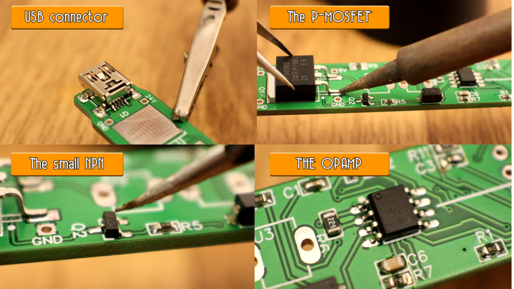
Poor contact occurs among the card slot and golden finger of printed circuit board, breakoff happens on cabled twist through the internal barrier, bad contact on wire cord and/or terminals, components lead COLD SOLDERING on the metal pad of printed circuit board;
(2) Signal interference:
For digital circuits, failure will be presented under certain condition, there may indeed be too much interference affecting the control system, but also parameters of the individual component and/or overall performance parameters of circuit board have changed, so that failure occurs result from the interference ability tends to the critical point.
(3) Thermal stability of parts:
From great amount of repairing practice and experience, electrolytic capacitors present the worst thermal stability, followed by the other capacitor, transistor, diode, IC, resistors, etc.;
(4) Residue on the PCB circuit board:
Moisture, dust and other residue on the surface of printed circuit board are conductive with a resistance effect, this resistance value will also change in the process of thermal expansion and contraction, the resistance value will have parallel effect in conjunction with the other components, the circuit parameters will be changed once the effect become stronger and caused failure occurs.
PCB Recreation Software Selection
How to judge if a PCB Recreation software is good or not, it is mainly depends on whether the function is complete or not, it is best to have all the work done within the software which will effectively increase the efficiency, include complete component library.
Protel 99SE can be viewed as a very outstanding one due to its component library is abundant, furthermore, it can download and upgrade the library from internel simutaneously to keep it updated consistently. This is very critical since the era of hand-drawing component when recreate circuit board has already passed, especially for those component with BGP package would cost far more than establishing library from the network automaticly.
In order to ensure the whole circuit system can be reliable and stable, designer should have large area of copper connect to POWER or GROUND layer which can decrease the impact of circuit noise and interference, so it will refers to the copper circuit network establishment issue. For a Printed Circuit board with extreme complicate network, there are lots of area need to be isolated or be connected, so we have to difine the network segment of different area and follow the principle as CONNECT SAME NETWORK segment & ISOLATE DIFFERENT NETWORK segment, just simply add copper into different network segment will cause short circuit easily.
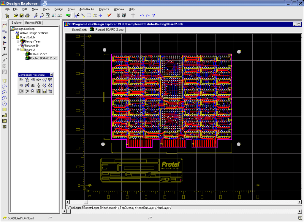
Currently the most popular printed circuit board recreation software in the market is PROTEL 99SE, the other is QUICKPCB 2005 Ver 3.0 plus some other colorful PWB Recreation softwares. Protel 99SE is a kind of EDA design software which is applicable by operating system like WINDOW 9X/2000/NT, it has design library management system, it can instruct networking design and coordination, has very strong data exchange capabilities, and 3D model simulation capabilities, a 32-bit design software, you can complete the extracted PCB board circuit schematic design, printed circuit board design and programmable logic device design, etc., can be designed up to 32 signal layers, 16 power supply – ground layers and 16 machining layers.
The operation of QUICKPCB 2005 Ver 3.0 is in line with the majority of designers operating practices, can greatly enhance the efficiency of pcb card cloning, 1st time circuit board recreation passing rate can be further guaranteed.
Software features
Place the pads, holes, lines, arcs, vias, components, FILL, POLYGON, text;
The element attribute settings, grid settings;
Automatically capture the CTRL key element of the grid with the center;
SHIFT key to select, to select, cut, copy, delete, rotate, mirror and repeat functions;
32 level set function, Zoom;
PCB Modification Process
PCB Modification is a Process to re-edit the circuit board layout drawing, which can be converted to gerber file, and make improvement over the schematic diagram of printed circuit board after extract the schematic from it;
There is a 4 layer Printed Circuit Board need to being modified, all the components assembled on the surface have already been removed, PCB surface being cleaned, the process of acquire Printed circuit board gerber file for production through printed circuit board reverse engineering can be seen below:
1 Scan TOP layer circuit board, save the scanning picture and name as TOP.jpg, the DPI value can be set according to the density of PCB card, hereby we choose 400DPI as reference; Scan Bottom layer and name it as BOTTOM.jpg; Use sand paper to abrade the TOP layer copper and expose the 2nd layer copper circuit pattern, scan the circuit pattern after clean it out and name it as MID1.jpg; Use sand paper to abrade the 2nd layer copper and expose the 3nd layer copper circuit pattern, scan the circuit pattern after clean it out and name it as MID2.jpg;
2 Open PCB Board reverse engineering software, click on “file” from MAIN MENU, and then click “OPEN BMP”, select the TOP.bmp file and open it, set up DPI value and then choose the PCB Card layer feature as TOP layer, start to place components, through-hole and arrange PCB Card circuit line, after you have arranged everything on the TOP layer, save file as temporary and name as TOP-1.dpb ( save the files periodically under different name such as TOP-2, TOP-3, TOP-4 prevent files lost from unexpected power cut-off or computer breakdown );
3 Hereby comes to the final step of circuit card modification from a 4 layer circuit board.
Click on “file” from MAIN MENU, and then click “OPEN BMP”, select the BOTTOM.bmp file, at the same time open temporary file TOP-1.dpb, and you will find that circuit card TOP layer picture which has been finished already can’t align to circuit board BOTTOM layer background picture, so you have to use cursor “UP”, ”DOWN”, ”LEFT”, ”RIGHT” to move its location, now you can choose some reference points to align the layers and after you have finished alignment you can start to place components, through-hole and arrange circuit line on BOTTOM layer, what if circuit line on the TOP layer block your eyesight on BOTTOM layer? It is easy, just from the main menu “Options” select “layer color settings”, cancel the selection of TOP layer as well as silkscreen, after you have arranged everything on the BOTTOM layer, save file as temporary and name as BOTTOM-1.dpb, or as BOTTOM-1.pcb;
Repeat the process you have just been through then can output completed circuit card file from circuit card modification.
4 Steps Help To Simplify PCB Repair Process
Under the circumstance of the absence of circuit schematic diagram, if you intend to repair a stange and complex faulty PCB circuit board, so called ”maintenance experience of PCB repair” can’t take its effect anymore, Even the veteran electronic technology hardware repair personnel get half the result with double the effort, so what can be done to better improve the repair efficiency? The following principles will make the repair task being finished in an orderly and smooth way:
1 Visual inspection before any movement:
Inspect the PCB circuit board ready for repair visually first, take the advantage of magnifying glass when necessary; at this point you have to emphasis on:
- Whether there is an existence of OPEN or SHORT circuit, especially checking if the connecting wires of printed circuit board have occurred disconnecting and adhesive;
- Whether there is an existence of disconnection of component lead like resistor, capacitor, inductor, diode and transistor;
- If the PCB circuit board has been repaired, and if the components on it being modified already?
And whether show the existence of cold solder,no solder and wrong/reverse component?
After all the conditions described above being excluded, now can use the multimeter to test the resistance value among power layer and ground layer, normally speaking the value shouldn’t less than 70Ω, if the resistance value less than that, for instance, only a few or a dozen ohms, that can illastrate that component(s) being breakdown, and then measure should be taken to find out what component(s) being breakdown, the most direct measure is supplying electric power to the circuit board (Note!!! Before that you have to figure out the working voltage and postive/negative polarity of the circuit board, the voltage must not allow higher than specified working voltage, otherwise circuit board will be damaged by it), point-temperature tester being applied to test the temperature of each component, the one whose temperature rise significant would be viewed as highly suspect item.
Once we can confirm the resistance value is normal, multimeter should be used again to test the diode, transistor, FET and bandswitch, etc. The purpose of all these actions is to ensure all the components tested are all normally function. Don’t let the problem go further and become complicate if it only need multimeter to address it.
2 Check exterior and then interior:
When you inspect the PCB circuit board by using on-site circuit repair tester, it is more preferable that you can have a same normal function PCB circuit board in hand for reference, through which you can make the comparison test among these 2 PCB circuit boards by VI curve scanning function, PCB circuit board connector can be viewed as the starting point and then go further, especially for capacitor testing, which can solve the problem that multimeter can’t if capacitor is leakage or not.
3 From easy to difficulty:
Before use on-site circuit maintenance tester to test the PCB circuit board, in order to ensure the accuracy, technical treatment can be done in advance to avoid the interference occurred during the testing, measures see below:
- Preparation before testing
Make the crystal become SHORT circuit ( please be noted you have to clarify which 2 pins are the signal output pins and then make them SHORT circuit, under this condition the 2 other power pins must not be shorted of 4 leads crystal ), for those electrolytic capacitor, you have to make it become SHORT circuit first, because charging and discharging large-capacitance electrolytic capacitor will have interference too.
- Elimination method for component test:
When use the on-site circuit maintenance tester to inspect all the components on the PCB circuit board, if the components pass the test and/or test result show it is normal, you can confirm the test result directly and make the record, for those fail to pass the test and/or test result show it is abnormal, test them one more time and if they still fail to pass the test then you can confirm the test result first, follow these ways and keep on testing all the components untill finish all the component test.
For those fail to pass the test, some testers have provided some very practical approach: this kind of tester can provide power supply to PCB circuit board through its clips, so in the same way it can supply power to component’s POWER and GROUND pins, if lift the POWER pin of component from PCB circuit board manually then this component will be out of the power supply system of PCB circuit board.
At this time use the on-site tester to inspect component, because the other components can’t being supplied by power so it will eliminate the interference effect and the testing circumstance equals to “quasi-off test”, the percent of accuracy can be improved significantly.
- Use ASA-VI intelligent curve technology can be applied to the comparison test of any component, as long as the component can be griped by test folder and moreover an reference PCB circuit board. Through comparison test it can also have strong fault detection and estimation ability, this feature offset the insufficiency of component library when operating on-site inspection, at the same time fault detection range has been extended effectively. Unfortunately in the reality the reference PCB circuit board usually can’t be found, and the electronic schematic structure of PCB circuit board ready to be repaired don’t have any symmetry, under this circumstance even the ASA-VI intelligent curve technology can’t have positive effect, and as a result of insufficiency of component library, the on-site testing can’t inspect each component on the PCB circuit board.
4 From static to dynamic
Because on-site circuit maintenance tester can only inspect the components assembled on PCB circuit board and have the static characteristic analysis, therefore the way to conclude that whether the faulty PCB circuit board has been completely repaired is install it back to the original equipment and then test-run the equipment. Under this circumstance all the power supply of this equipment should be checked and ensure it can correctly provide power to the PCB circuit board, moreover all the connectors on it have been installed in good condition, the negative impact of incorrect connection of PCB circuit board must be eliminated completely.
PCB Repair Inspection Flow
Step 1: Ask customer about the breakerdown appearances of damaged electronic device as well as on-site situation;
Step 2: Analyse the root cause of breakdown according to customer description;
Step 3: Dissemble device and clean it thoroughly; confirm the components being damaged and then assess the feasibility of can-be REPAIR;
Step 4: Analyse the circuit schematic diagram according to the location of damaged components, find out the root cause of components being damaged and prevent similar situations happen again;
Step 5: Communicate with customers about the components list that need to be replaced, collect comment from customer, start Repairing after receipt of customer confirmation on quote;
Step 6: Repair service include eliminate the existing problems and faults, replace obselete or damaged components, clean the entire device thoroughly and required maintenance;
Step 7: Instruct SIMULATIVE LOAD TEST after repairing process finish, once pass the test will send to customer for further on-site testing.
PCB Relayout Capabilities
PCB Relayout can also be defined as circuit board schematic diagram modification through which the electrical and electronic performance of printed circuit board will be improved;
—- We can handle single sided, double sided, multilayer up to 20 layers PCB Relayout;
—- No limit on nodes, holes and pads, holes refers to PCB Board with Blind & Buried via down to 0.1mm;
—- Circuit Board size range from 546*622mm due to the capability limitation, over that size;
—- No limitation on components type (through hole, surface mount, or mixed);
—- SMT pitch down to 0.2mm or less depending on board layout;
—- Application refers to Measurement, Telecommunication, Networking, Consumer Electronics, Industrial Automation;
Service Deliver:
We can send your emails containing all the information and files you need to remanufacture your electronic PCB card:
1 Schematic diagrams and drawing files; (Optional)
2 Bill of materials (BOM) list all components as well as individual description;
3 PCB plate Gerber files and drilling/outline files for the prototype or mass production;
4 Optional: A fully functional prototype PCB Assembled with all components as-specified for testing and evaluation.
PCA Reverse Engineering Introduction
PCA Reverse Engineering, also known as printed circuit board redesigning, is using clone technology onto the PCA which was designed and manufactured by others, it is to use PCB with mounted components related software to copy someone else’s PCA and then manufacture it by yourself.
This is the tradditional explanation for circuit card reverse engineering. with the PCB reverse engineering technology development, the impact and scope of this industry continues to expand rapidly, and the definition of PCB board reverse engineering also extend from the narrow sense that: PCB card clone only refers to extraction of PCB file from electronic circuit board and then restore it;
To the wide sense that pcb clone not only include PCB file extraction, Circuit Board Reverse Engineering and other related technical aspect, but also modify PCB file, the shape of the mold for electronic products, extraction of 3-dimensional model data on a variet of electronic products, compile the components list assembled on the PCA as well as individual data sheets on each component where available, decrypt microcontroller on the circuit board, crack encrypted IC on the PCB, moreover, inverse assemble the firmware of PCA Board and etc, a whole set of circuit board restoration technology.