 Attack MCU Method Introduction
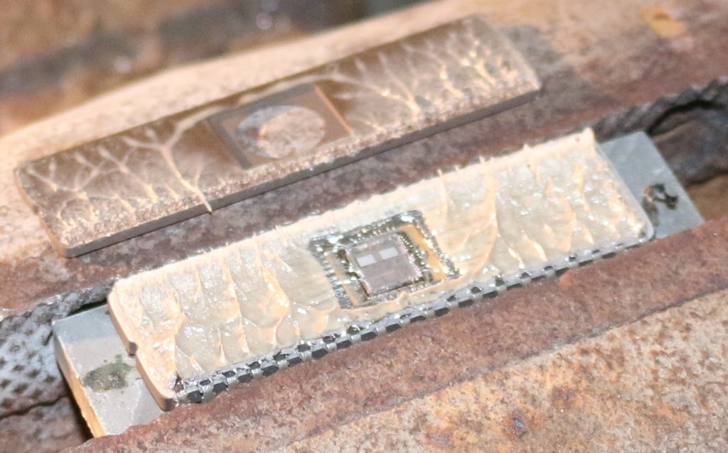
Attack MCU Method can be categorized with invasive and semi-invasive ones, through which will be able to extract code from IC chip and make microcontroller clone;
1 — Software MCU Attack:
This method use communication interface of processor plus protocol, encrypted algorithm to attack microcontroller, a typical successful example of software attack is the breaking against early MCU ATMEL AT89C51 series MCU. Attacker takes advantage of the design flaw of erasure operation sequence, use self-made program to erase encrypted lock location, and then halt the next operation of erase internal program, through which the encrypted MCU being turn into decrypted MCU after attacked, finally use programmer to read the internal procedure.
Currently base upon the other encryption method, some kind of devices can be promoted accompany with certain types of software can be used as software mcu attack. In recent days, domestic market has presented a kind of 51 MCU cracking device, this decipher is mainly focus on brands like SyncMos, Winbond, use the leak of the production technology and insert positioning bit of several programmer, find out continuous empty locations through certain methods, which means need to find out the continuous FF FF bits, those inserted bits can instruct the order of send internal program to outside environment, and then use processor attack device to intercept and capture.
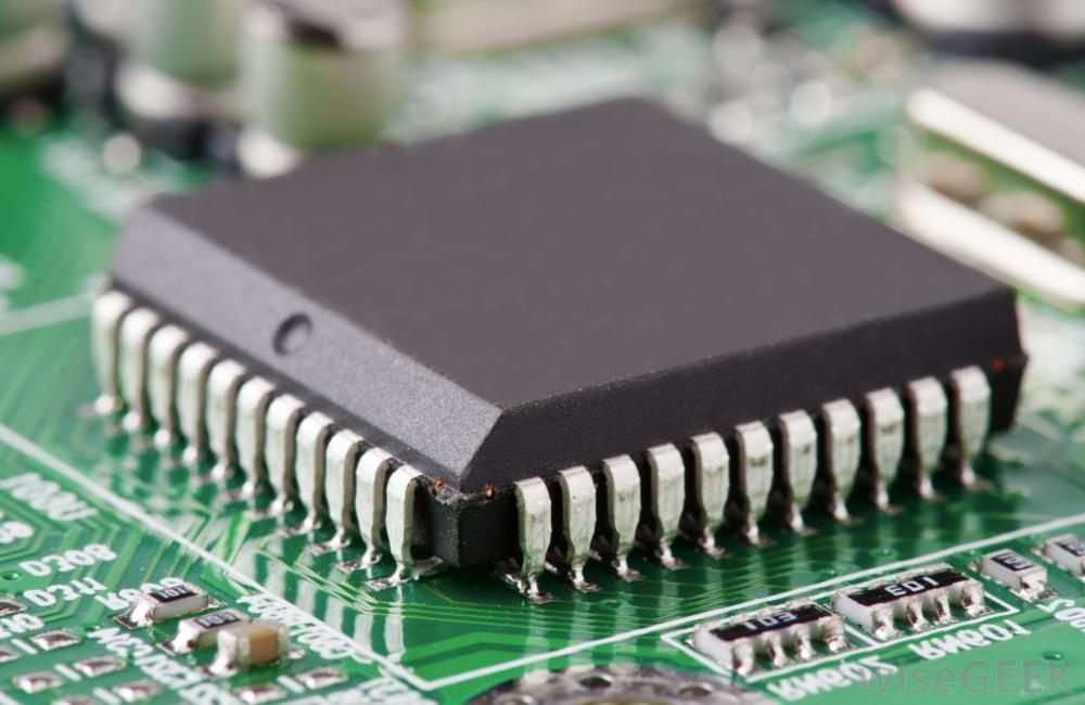
MCU Break Introduction
MCU Break is a process to disable the secured protection against unauthorized MCU reading, focus ion beam technique will be applied to remove the fuse bit to expose the flash memory;
Microcontrollers generally have internal EEPROM / FLASH program for users to store data. To prevent unauthorized access or copy microcontroller program of MCU (MCU crack), most of MCUs are encrypted with the encryption lock orientation or lock-bit bytes to protect the MCU program.
If the programming lock-bit encryption is enabled (locked), you can’t use ordinary programmer reads the program directly within MCU, which is called encryption or MCU locking.
MCU IC breaker with special equipment or home-made equipment, take the advantage of single IC design flaw or software defects, through a variety of techniques, can attack key information from the MCU, access to program inside microcontroller, which is called microcontroller break.
Please view our service procedures below for your reference:
Step 1:
After recipient of original MCU from customer and finish the electrical integrity test to confirm the feasibility of work, official invoice will be sent from us, customer prepay 50% payment, we start the project upon the confirmation of payment recipient;
Step 2:
After process finish and informed by us, program will be loaded into two pieces of new empty MCUs and send back to customer for verification, customer need to pay freight cost and new MCU samples cost in advance;
Step 3:
Customer has obliged to inform the test result within 5 working days after receipt of programmed MCU samples, if test is passed, customer need to pay the balance within 72 hours and we will send the program to customer through email after confirm the receipt of customer balance payment within 48 hours;
Step 4:
If the samples don’t work, it is obliged to take necessary evaluation after the receipt of functionality testing platform for debugging and resubmit samples within 3 weeks, and if still fail to find and solve the problems, we have to refund customer all of prepayment within 2 weeks upon the date of mutual agreement. (Include MCU samples price and freight cost).
If you have any further inquiry regarding our service please feel free to let us know, thanks
2 Different Amplifier
2 Different Amplifier
Different amplifier can only magnify the D-VALUE of 2 signals, but won’t magnify general voltage signal. If design job of different amplifier and Printed Circuit Board aren’t reasonable, when signal level in the low status, general voltage will generate a small differential interference signal. Due to the high input impedance of different amplifier, any parameter imbalance on input point will bring much great interference to circuit. Therefore, during the printed circuit board design process, it has to ensure physical structure of amplifier complete symmetry.

There is a leakage resistance exist in the input point of different amplifier, it can take an effect of imbalance voltage deviation. Designer can solve this problem through add protective device on the input circuit, protective device can circle the signal wire, if it can keep the same voltage with 2 input signal low level, as a result of that, positive resistance value will increase. This device can ensure signal source terminal and protector keep the same voltage with low level of signal source.

1 High gain DC amplifier
High gain DC amplifier generally being used to amplify small signal. When crystal transistor or DC amplifier being soldered on PCB Board, thermocouple will be formed between copper layer and component lead, therefore will occur different AC voltage, it will has interference signal against amplifier. In order to keep the minimum temperature fluctuation rate around DC amplifier INPUT point, and remain the balance, we suggest to separate INPUT point with part to avoid the influence caused by air flow.
Reasonable Analog Signal Circuit Layout in the PCB Board
In the analog circuit PCB Board, signal circuit can fulfill a variety of functions, such as signal input, feedback, output and provide standard signal. Therefore, refers to different applications, signal circuit must be optimized through different ways. However, there is an commonly known principle that in all the analog circuit PCB Board, signal circuit should be as short as possible, that is because the longer signal circuit, the more chances it can involve inductance and capacitor, that is the last thing PCB design engineer want to see. But the fact is impossible to make all the signal circuit to its shortest level. Therefore we have to take the most readily having interference signal circuit layout into account.
Below signal circuit layout need particular attention during PCB layout:
1> High frequency oscillator / amplifier;
2> Multi-level amplifier, especially with high output power;
3> High gain DC amplifier;
4> Minor signal amplifier;
5> Differential amplifier;
Which method is better for PCB Layout, manually or automatically?
If we choose to use auto layout, till which level it can support? Such as how many layer it can be? What frequency it can achieve?
All the PCB designers I have ever encountered prefer to choose layout PCB manually, because they say the auto-layout don’t have good result compare with layout manually. From my point of view, IC layout is more difficult and complicate than PCB layout, but why IC layout can use auto-layout nor PCB?
Precisely speaking, no matter auto-layout or manual-layout, there should be a principle ahead, that is: rule driven. Those designers who claim that auto-layout is not good because most of the rules are still embedded in their mind, and haven’t yet integrate into the design, so the auto-layout won’t achieve their requirement.
Frankly speaking, the rule set up for auto-layout can’t be achieve 100%, so after PCB Layout finish, we still need to modify it manually.
So there is a balance among here, if the time you spend on integrate the rule into software has already longer than the time have been taken for PCB layout manually, it is not necessary to make auto-layout.
So few designers auto-layout high frequency, because almost every line of high frequency PCB has restriction, so if we need to add rule to each network, there surely more time we need to spend than manually layout.
Common component PROTEL package list 2
Most commonly Resistor package datasheet of PROTEL SE
Resistor: AXIAL0.3-AXIAL0.7, 0.4-0.7 stands for resistor length, normal version is AXIAL0.4.
PROTEL SE DIODE package datasheet
Ceramic capacitor: RAD0.1-RAD0.3, 0.1-0.3 stands for size of capacitor, normal version is RAD0.1;
Electro: RB.1/.2-RB.4/.8, .1/.2-.4/.8 means the value of capacitor. Normal if below 100uF will use B.1/.2,100uF-470uF choose RB.2/.4, larger than 470uF use RB.3/.6.
Diode: Diode 0.4-Diode 0.7, and 0.4-0.7 means the length of diode, normally use Diode 0.4: RB .1/.2.
Integrated Circuit: DIP8-DIP40, 8-40 means the quantity of pins, 8 pins stand for DIP8.
PROTEL SE SMD resistor
0603 stands for the package size, no relations with concrete value;
But the package size and power do have some relationship as below:
0201 1/20W
0402 1/16W
0603 1/10W
0805 1/8W
1206 1/4W
The relations among capacitor size and package see as below:
0402=1.0×0.5
0603=1.6×0.8
0805=2.0×1.2
1206=3.2×1.6
1210=3.2×2.5
1812=4.5×3.2
2225=5.6×6.5
Refers to the component package we have mentioned before, except those components inside the DEVICE.lib database, components in other databases are all have fixed package format, that is because components in the library has different kinds of format: take the transistor as reference, it is one of the most commonly used components, in the DEVICE.lib database there is only simple difference between NPN and PNP. Actually, if it is 2N3055 of NPN, then it probably TO-3, if it belongs to 2N3054 of NPN, then it probably TO-66 or TO-5, also for CS9013 we have TO-92A, TO-92B, TO-5, TO-46, TO-52.
Another one is capacitor, in the database of DEVICE, it can be simply called as RES1 & RES2, no matter is could be 100Ω or 470KΩ, they could be the same. As for circuit board, it can use has no relation with OHM value, just depends on power value of the resistor to decide if we choose 1/4W or 1/2W, and all of them can use AXIAL0.3 component package. If the power value larger than normal we can choose AXIAL0.4, AXIAL0.5 etc. now we list most commonly used component package as below for your reference:
Resistor and non-polarity double end component: AXIAL0.3-AXIAL1.0
Non-polarity capacitor: RAD0.1-RAD0.4
Polarity capacitor: RB.2/.4-RB.5/1.0
Diode: DIODE0.4 and DIODE0.7
Common component PROTEL package list 1
Component package means the cosmetic performance and soldering point location on the circuit board when it is being assembled, it is definitely space concept. So different components can use same package, same components do have possibility to apply different package. Like Resistor, has traditional DIP package, these kinds of components usually have large size, circuit board must be drilled before assemble, after drilling and insert the components, pass through solder tin oven or manual soldering, the cost could be high, updated designs are all applied small size SMD component, this type of package don’t need drill hole, use stainless stencil as silkscreen to pour solder tin onto surface of circuit board and then place SMD component on it for assembly.
Most common component package datasheet:
RES1,RES2,RES3,RES4;feature is axial series;
RAD:cap; feature is RAD-0.1 to RAD-0.4
Electro; feature is RB.2/.4 to RB.5/1.0
Potentiometer:pot1,pot2;feature is VR-1 to VR-5
Diode:feature is diode-0.4 (low power)diode-0.7 (high power)
Triode:common feature is to-18, to-22(high power triode)to-3(high power NPN)
Regulated power supply has 78 and 79 series;78 series include 7805,7812,7820, etc.
79 series has 7905,7912,7920 etc.
Most common package include TO-126h and TO-126v
Rectifier bridge:BRIDGE1,BRIDGE2: package feature D series(D-44,D-37,D-46)
Dual probe and Flying probe test
Flying probe doesn’t rely on the pin drawing fixed on fixture. Two or more probes can be installed on the surface of X-Y and move freely, the testing point can be controlled by CAD GERBER FILE. Dual probe can move within 4 mil area. Probe can move isolated, also at the same time didn’t restrict the real distance of how close they can be. Testing device with 2 moving hands is base upon capacitor, press PCB on the insulation layer of a metal sheet as the capacitor for another metal sheet. In case there is 1 wire happen to short, capacitor value will become larger then certain point; if there is a open wire, capacitor will become smaller.
PCB Schematic Diagram Design proces
The design of schematic diagram should use SCHEMATIC DIAGRAM design system of PROTEL98 or PROTEL99SE to draw a schematic diagram, it is the foundation of circuit board design project. During this process, designer should take advantage of all kinds of drawing tools and edit functions provided by software, the process is see below:
1. Start-up: open up PROTEL98 schematic diagram editor:
Click “Start” bottom, and choose PROTEL98 inthe “Program”.
2. Install circuit drawing dimension and layout
User can install the dimension, orientation and grid size of drawing and title.
3. Place necessary components on the schematic diagram
User select the necessary components from database and place them onto the right place according to circuit schematic diagram requirement, as well as modification.
4. Layout the components which have been placed
Use line and signal to connect all the components on platform to constitute a complete schematic diagram
5. Modify components after PCB layout
In order to ensure the schematic diagram’s preciseness and aesthetic, components location need to be modify through delete, move and adjust drawing size, feature and orientation.
6. Save file and print output
Save schematic diagram which has been edited and print it out for file.