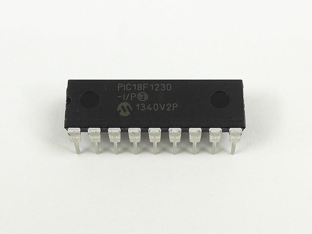
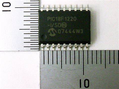
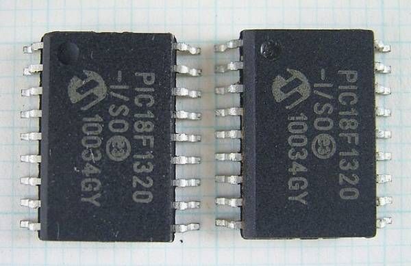
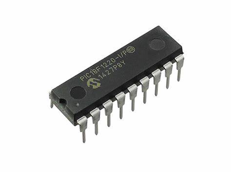
 Decrypt Locked PIC18F1230 Microcontroller Flash Memory
Decrypt Locked PIC18F1230 Microcontroller Flash Memory and extract embedded code from mcu pic18f1230 flash memory, the binary file of pic18f1230 microprocessor will be readout directly;
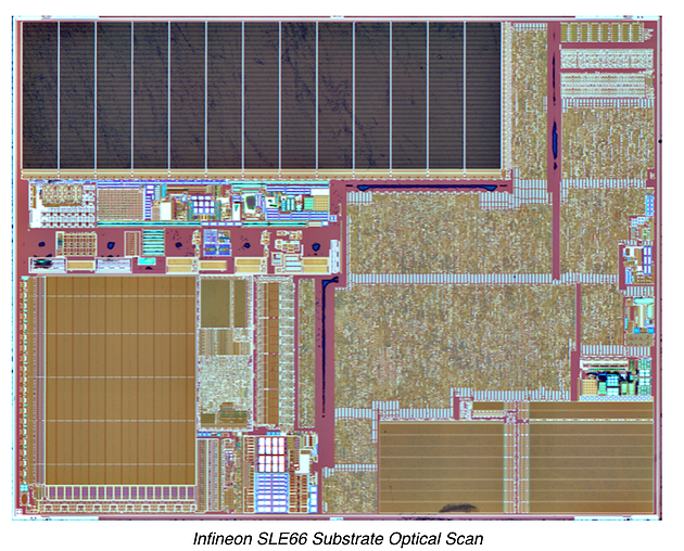
Devices in the PIC18F1220/1320 family are available in 18-pin, 20-pin and 28-pin packages. A block diagram for this device family is shown in Figure 1-1. The devices are differentiated from each other only in the amount of on-chip Flash program memory when decaps microchip pic18f1320 processor flash memory (4 Kbytes for the PIC18F1220 device, 8 Kbytes for the PIC18F1320 device).
descriptografar a memória flash do microcontrolador PIC18F1230 bloqueado e extrair o código incorporado da memória flash mcu pic18f1230, o arquivo binário do microprocessador pic18f1230 será lido diretamente
The PIC18F1220 and PIC18F1320 devices can be operated in ten different oscillator modes. The user can program the Configuration bits, FOSC3:FOSC0, in Configuration Register 1H to select one of these ten modes:
- LP Low-Power Crystal
- XT Crystal/Resonator
- HS High-Speed Crystal/Resonator
- HSPLL High-Speed Crystal/Resonator
with PLL enabled
- RC External Resistor/Capacitor with
FOSC/4 output on RA6
- RCIO External Resistor/Capacitor with
I/O on RA6
- INTIO1 Internal Oscillator with FOSC/4
output on RA6 and I/O on RA7
- INTIO2 Internal Oscillator with I/O on RA6
and RA7
- EC External Clock with FOSC/4 output
ECIO External Clock with I/O on RA6
In XT, LP, HS or HSPLL Oscillator modes, a crystal or ceramic resonator is connected to the OSC1 and OSC2 pins to establish oscillation. below Figure shows the pin connections. The oscillator design requires the use of a parallel cut crystal.
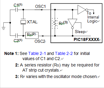
RESONATOR OPERATION (XT, LP, HS OR HSPLL CONFIGURATION)
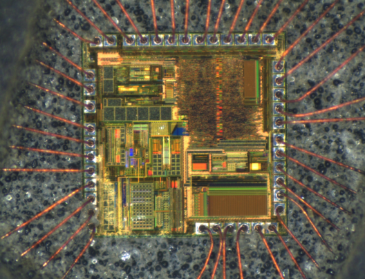
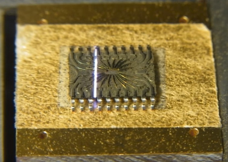
Microchip PIC18F1220T Processor Memory Restoring
Microchip PIC18F1220T Processor Memory Restoring including cracking mcu pic18f1220t security fuse bit by focus ion beam, and then copy heximal file to new microcontroller pic18f1220t;
- Memory Endurance: The Enhanced Flash cells for both program memory and data EEPROM are rated to last for many thousands of erase/write cycles – up to 100,000 for program memory and 1,000,000 for EEPROM. Data retention without refresh is conservatively estimated to be greater than 40 years.
- Self-programmability: These devices can write to their own program memory spaces under internal software control. By using a bootloader routine located in the protected Boot Block at the top of program memory by decoding pic18f1220 microcontroller firmware, it becomes possible to create an application that can update itself in the field.
- Enhanced CCP module: In PWM mode, this module provides 1, 2 or 4 modulated outputs for controlling half-bridge and full-bridge drivers. Other features include auto-shutdown, for disabling PWM outputs on interrupt or other select conditions and auto-restart, to reactivate outputs once the condition has cleared.
- Enhanced USART: This serial communication module features automatic wake-up on Start bit and automatic baud rate detection and supports RS-232, RS-485 and LIN 1.2 protocols, making it ideally suited for use in Local Interconnect Network (LIN) bus applications.
Microchip PIC18F1220T processador de restauração de memória, incluindo rachaduras mcu pic18f1220t segurança fusível bit a feixe de íons de foco e, em seguida, copiar arquivo heximal para o novo microcontrolador pic18f1220
10-bit A/D Converter: This module incorporates programmable acquisition time, allowing for a channel to be selected and a conversion to be initiated without waiting for a sampling period and thus when extract pic18f1220 mcu source code, reduce code overhead.
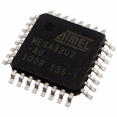
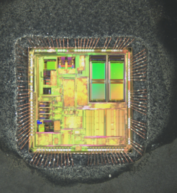
Attack ATMEGA32U2-MU Microprocessor Fuse Bit
Attack ATMEGA32U2-MU Microprocessor Fuse Bit and unlock secured atmega32u2 processor protection over its embedded flash memory heximal, and then extract source code from atmega32u2 mcu;
The period of the Watchdog Oscillator is 1 µs (nominal) at 5.0V and 25°C. The frequency of the Watchdog Oscillator is voltage dependent as shown in “Electrical Characteristics – TA = -40°C to 85°C” on page 232.
The MCU will wake up if the input has the required level during this sampling or if it is held until the end of the start-up time. The start-up time is defined by the SUT Fuses as described in “System Clockand Clock Options” on page 31.
If the level is sampled twice by the Watchdog Oscillator clock but disappears before the end of the start-up time, the MCU will still wake up, but no interrupt will be generated to recover atmega32 mcu flash program and eeprom data. The required level must be held long enough for the MCU to complete the wake up to trigger the level interrupt.
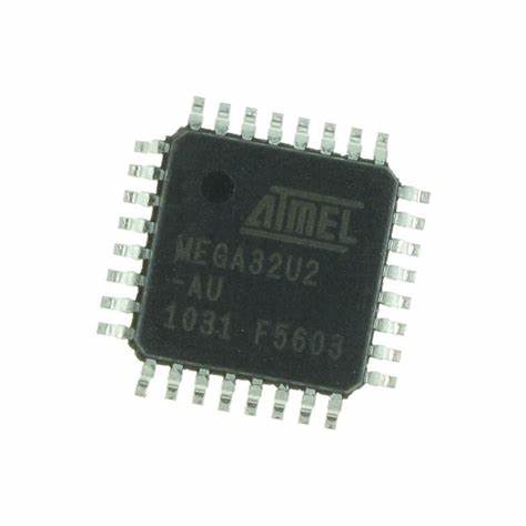
Attack ATMEGA32U2-MU Microprocessor Fuse Bit and unlock secured atmega32u2 processor protection over its embedded flash memory heximal, and then extract source code from atmega32u2 mcu
The MCU Control Register contains control bits for interrupt sense control and general MCU functions. The External Interrupt 1 is activated by the external pin INT1 if the SREG I-bit and the corresponding interrupt mask in the GICR are set. The level and edges on the external INT1 pin that activate the interrupt are defined in Table 14-1.
The value on the INT1 pin is sampled before detecting edges. If edge or toggle interrupt is selected, pulses that last longer than one clock period will generate an interrupt when restoring atmega32l microprocessor memory software. Shorter pulses are not guaranteed to gener- ate an interrupt. If low level interrupt is selected, the low level must be held until the completion of the currently executing instruction to generate an interrupt.
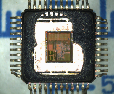
Break ATMEGA32U2-AU Microcontroller Flash Memory
Break ATMEGA32U2-AU Microcontroller Flash Memory and clone microprocessor memory data to new atmega32u2 chip, the embedded software will be readout from mcu atmega32u2;
This is set up as indicated in the specification for the MCU Control Register – MCUCR. When the external interrupt is enabled and is configured as level triggered, the interrupt will trigger as long as the pin is held low.
Note that recognition of falling or rising edge interrupts on INT0 and INT1 requires the presence of an I/O clock when reverse engineering atmel avr chip atmega32a program file, described in “Clock Systems and their Distribution”.
Low level interrupts on INT0/INT1 are detected asynchronously. This implies that these interrupts can be used for waking the part also from sleep modes other than Idle mode. The I/O clock is halted in all sleep modes except Idle mode.
quebrar ATMEGA32U2-AU microcontrolador de memória flash e clonar dados de memória de microprocessador para o novo chip atmega32u2, o software incorporado será lido a partir de mcu atmega32u2
Note that if a level triggered interrupt is used for wake-up from Power-down mode, the changed level must be held for some time to wake up the MCU in the process of recover protected atmega32 mcu memory. This makes the MCU less sensitive to noise. The changed level is sampled twice by the Watchdog Oscillator clock.
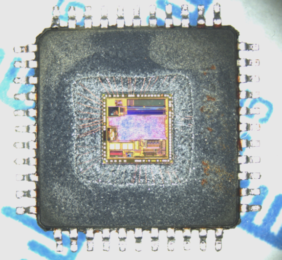
Decap Microchip PIC18F1320 Processor
Decap Microchip PIC18F1320 Processor and then extract flash and eeprom memory content from pic18f1320 mcu chip, the source code will be copied embedded firmware from pic18f1320 microcontroller flash memory,
All of the devices in the PIC18F1220/1320 family offer nine different oscillator options, allowing users a wide range of choices in developing application hardware. These include:
Four Crystal modes, using crystals or ceramic resonators.
Two External Clock modes, offering the option of using two pins (oscillator input and a divide-by-4 clock output), or one pin (oscillator input, with the second pin reassigned as general I/O).
Two External RC Oscillator modes, with the same pin options as the External Clock modes.
An internal oscillator block, which provides an 8 MHz clock (±2% accuracy) and an INTRC source (approximately 31 kHz, stable over temperature and VDD), as well as a range of six user-selectable clock frequencies (from 125 kHz to 4 MHz) for a total of 8 clock frequencies.
decap Microchip PIC18F1320 processador e, em seguida, extrair flash e eeprom conteúdo de memória de pic18f1320 mcu chip, o código-fonte será copiado firmware incorporado da memória flash do microcontrolador pic18f1320,
Besides its availability as a clock source, the internal oscillator block provides a stable reference source that gives the family additional features for robust operation:
Fail-Safe Clock Monitor: This option constantly monitors the main clock source against a reference signal provided by the internal oscillator. If a clock failure occurs by recovering pic18f1330 microchip mcu source code, the controller is switched to the internal oscillator block, allowing for continued low-speed operation, or a safe application shutdown.
Two-Speed Start-up: This option allows the internal oscillator to serve as the clock source from Power- on Reset, or wake-up from Sleep mode, until the primary clock source is available in the process of attacking pic18f13k50 microcontroller flash memory. This allows for code execution during what would otherwise be the clock start-up interval and can even allow an application to perform routine background activities and return to Sleep without returning to full-power operation.
Decode Secured PIC18F1220 Microcontroller Program
Decode Secured PIC18F1220 Microcontroller Program from its flash and eeprom memory, copy the firmware to new mcu pic18f1220 which will perform the same functions, original source code in the format of heximal will be extracted from processor pic18f1220;
This family offers the advantages of all PIC18 microcon- trollers – namely, high computational performance at an economical price – with the addition of high endurance Enhanced Flash program memory.
On top of these fea- tures, the PIC18F1220/1320 family introduces design enhancements that make these microcontrollers a logical choice for many high-performance, power sensitive applications when reverse engineering pic18f2580 microprocessor embedded software.
decodificar o programa microcontrolador PIC18F1220 protegido de sua memória flash e eeprom, copiar o firmware para o novo mcu pic18f1220 que executará as mesmas funções, o código-fonte original no formato de heximal será extraído do processador pic18f1220
All of the devices in the PIC18F1220/1320 family incor- porate a range of features that can significantly reduce power consumption during operation. Key items include:
- Alternate Run Modes: By clocking the controller from the Timer1 source or the internal oscillator block, power consumption during code execution can be reduced by as much as 90%.
- Multiple Idle Modes: The controller can also run with its CPU core disabled, but the peripherals are still active. In these states, power consumption can be reduced even further, to as little as 4% of normal operation requirements by recover pic18f2553 mcu flash heximal.
- On-the-fly Mode Switching: The power managed modes are invoked by user code during operation, allowing the user to incorporate power-saving ideas into their application’s software design.
- Lower Consumption in Key Modules: The power requirements for both Timer1 and the Watchdog Timer have been reduced by up to 80%, with typical values of 1.1 and 2.1 mA, respectively.
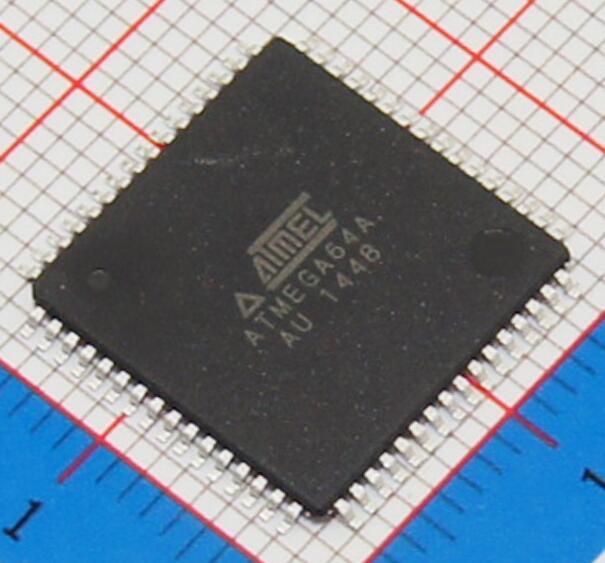
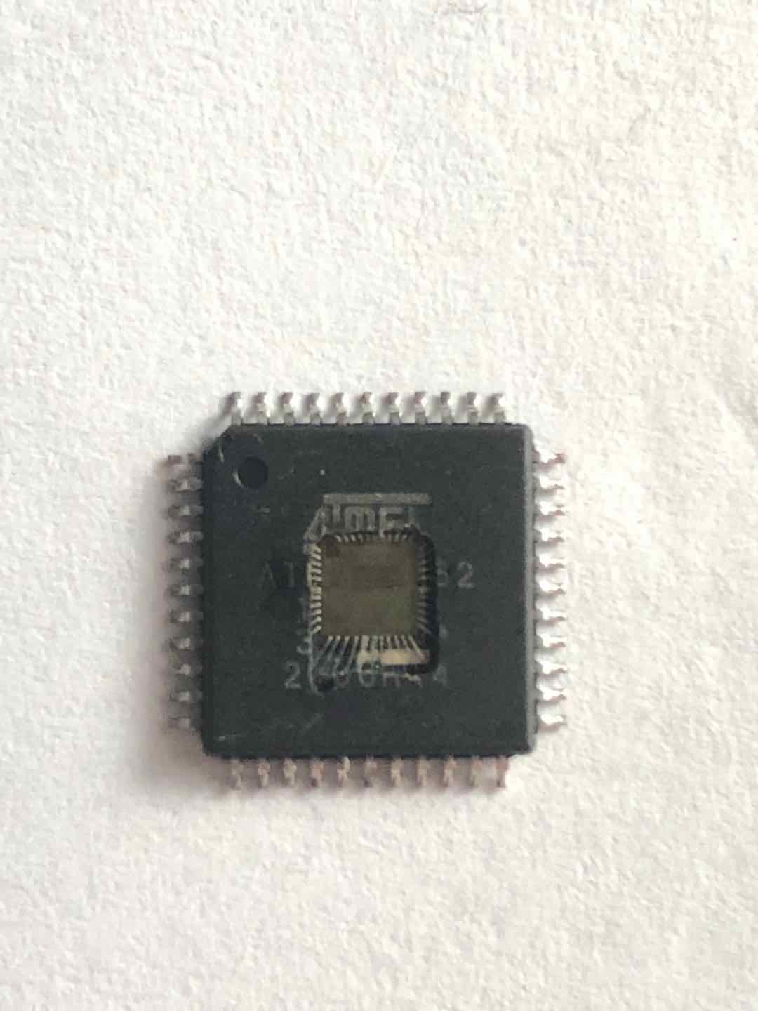
Decrypt Microcontroller ATMEGA64A Memory Data
Decrypt Microcontroller ATMEGA64A Memory Data is a process to recover avr atmega64a mcu embedded firmware and readout heximal file from processor atmega64a;
When switching between tri-state ({DDxn, PORTxn} = 0b00) and output high ({DDxn, PORTxn} = 0b11), an inter- mediate state with either pull-up enabled ({DDxn, PORTxn} = 0b01) or output low ({DDxn, PORTxn} = 0b10) must occur. Normally, the pull-up enabled state is fully acceptable, as a high-impedant environment will not notice the
difference between a strong high driver and a pull-up. If this is not the case, the PUD bit in the SFIOR Register can be set to disable all pull-ups in all ports when recover protected atmega32 mcu eeprom memory.
Switching between input with pull-up and output low generates the same problem. The user must use either the tri-state ({DDxn, PORTxn} = 0b00) or the output high state ({DDxn, PORTxn} = 0b11) as an intermediate step.
descriptografar microcontrolador ATMEGA64A dados de memória é um processo para recuperar avr atmega64a mcu firmware embutido e arquivo heximal de leitura do processador atmega64a
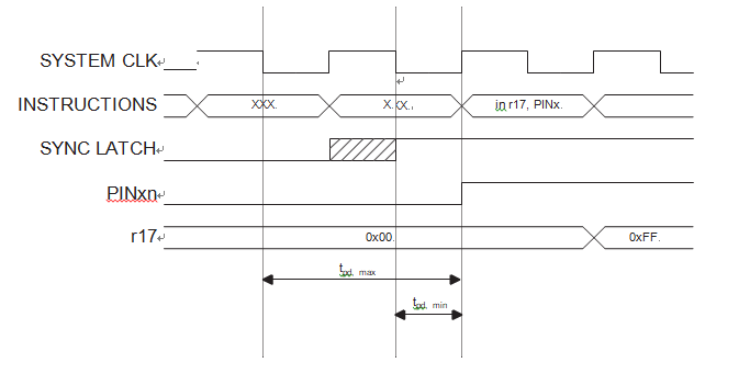
Independent of the setting of Data Direction bit DDxn, the port pin can be read through the PINxn Register Bit. As shown in Figure 13-2, the PINxn Register bit and the preceding latch constitute a synchronizer by restoring atmega32l microprocessor memory software. This is needed to avoid metastability if the physical pin changes value near the edge of the internal clock, but it also introduces a delay.
Below Figure shows a timing diagram of the synchronization when reading an externally applied pin value. The maximum and minimum propagation delays are denoted tpd,max and tpd,min, respectively.
Break ATMEGA64L Secured Microcontroller Flash Memory
Break ATMEGA64L Secured Microcontroller Flash Memory and clone the avr mcu atmega64l heximal content to new MCU, read the firmware program out from atmega64l microprocessor flash and eeprom memory;
Each port pin consists of 3 Register bits: DDxn, PORTxn, and PINxn. As shown in “Register Description” on page 69, the DDxn bits are accessed at the DDRx I/O address, the PORTxn bits at the PORTx I/O address, and the PINxn bits at the PINx I/O address.
The DDxn bit in the DDRx Register selects the direction of this pin. If DDxn is written logic one, Pxn is configured as an output pin when recover protective microprocessor atmega16 firmware. If DDxn is written logic zero, Pxn is configured as an input pin.
If PORTxn is written logic one when the pin is configured as an input pin, the pull-up resistor is activated. To switch the pull-up resistor off, PORTxn has to be written logic zero or the pin has to be configured as an output pin.
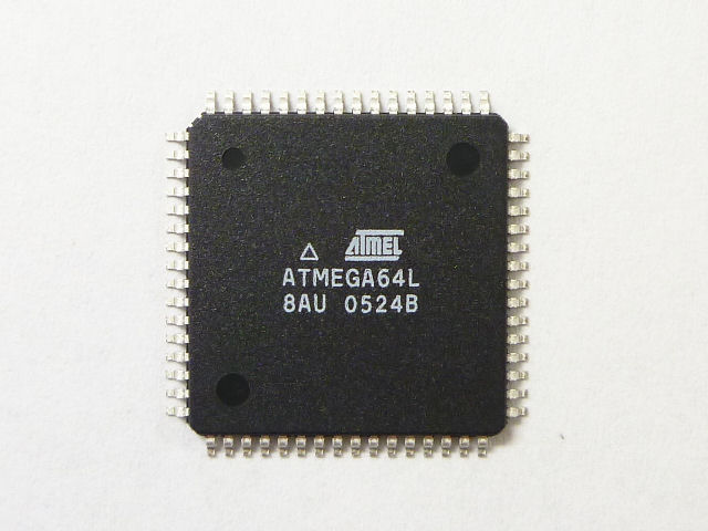
quebrar ATMEGA64L memória flash microcontrolador seguro e clonar o avr mcu atmega64l conteúdo heximal para novo MCU, ler o programa de firmware para fora do atmega64l microprocessador flash e memória eeprom
The port pins are tri-stated when a reset condition becomes active, even if no clocks are running. If PORTxn is written logic one when the pin is configured as an output pin to break atmega16l locked mcu flash memory, the port pin is driven high (one). If PORTxn is written logic zero when the pin is configured as an output pin, the port pin is driven low (zero).
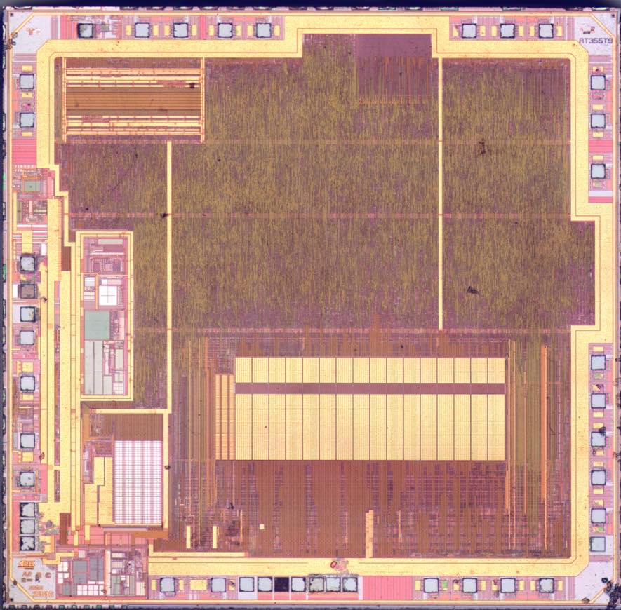
Reverse ATMEGA64 Microcomputer Flash Memory
Reverse ATMEGA64 Microcomputer Flash Memory and recover atmega64 mcu flash embedded heximal out from its flash memory and eeprom memory, read data out from microcontroller atmega64 memory;
If Interrupt Vectors are placed in the Boot Loader section and Boot Lock bit BLB02 is programmed, interrupts are disabled while executing from the Application section by breaking atmega16l locked mcu flash memory. If Interrupt Vectors are placed in the Application section and Boot Lock bit BLB12 is programed, interrupts are disabled while executing from the Boot Loader section.
The IVCE bit must be written to logic one to enable change of the IVSEL bit. IVCE is cleared by hardware four cycles after it is written or when IVSEL is written. Setting the IVCE bit will disable interrupts, as explained in the IVSEL description above.
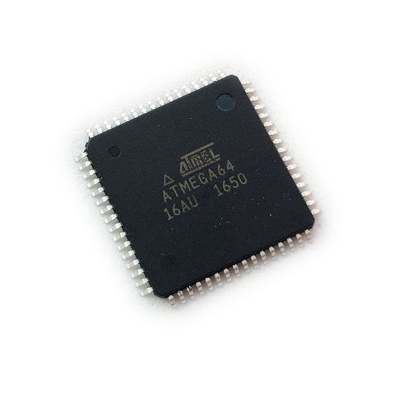
reverter a memória flash do microcomputador ATMEGA64 e recuperar atmega64 mcu flash embutido heximal para fora de sua memória flash e memória eeprom, ler dados fora do microcontrolador atmega64 memória
All AVR ports have true Read-Modify-Write functionality when used as general digital I/O ports. This means that the direction of one port pin can be changed without unintentionally changing the direction of any other pin with the SBI and CBI instructions in order to recover protective microprocessor atmega16 firmware. The same applies when changing drive value (if configured as output) or enabling/dis- abling of pull-up resistors (if configured as input).
Copy R5F212B7SNFP MCU Flash Memory
Copy R5F212B7SNFP MCU Flash Memory content needs to unlock renesas r5f21134fp mcu secured flash program, and then extract microcontroller r5f212b7s flash firmware;
In this mode, the Watchdog Timer is initially disabled, but can be enabled by writing the WDE bit to 1 without any restriction. A timed sequence is needed when changing the Watchdog Time-out period or disabling an enabled Watchdog Timer to dump renesas r5f212a7 protected mcu flash program. To disable an enabled Watchdog Timer and/or changing the Watchdog Time-out, the following procedure must be followed:
In the same operation, write a logic one to WDCE and WDE. A logic one must be written to WDE regard- less of the previous value of the WDE bit.
Within the next four clock cycles, in the same operation, write the WDE and WDP bits as desired, but with the WDCE bit cleared by .
In this mode, the Watchdog Timer is always enabled, and the WDE bit will always read as one. A timed sequence is needed when changing the Watchdog Time-out period when copying renesas locked microprocessor r5f212aasd memory data. To change the Watchdog Time-out, the following proce- dure must be followed:
copiar R5F212B7SNFP MCU conteúdo de memória flash precisa desbloquear renesas r5f21134fp mcu programa flash seguro e, em seguida, extrair microcontrolador r5f212b7s firmware flash
1. In the same operation, write a logical one to WDCE and WDE. Even though the WDE always is set, the WDE must be written to one to start the timed sequence.
Within the next four clock cycles, in the same operation, write the WDP bits as desired, but with the WDCE bit cleared. The value written to the WDE bit is irrelevant.