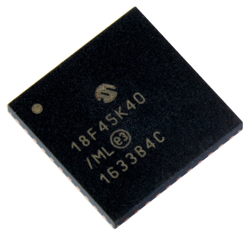
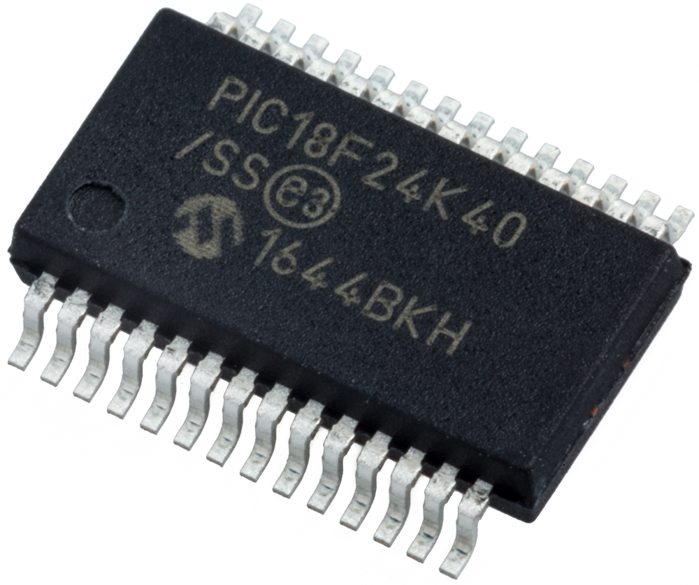
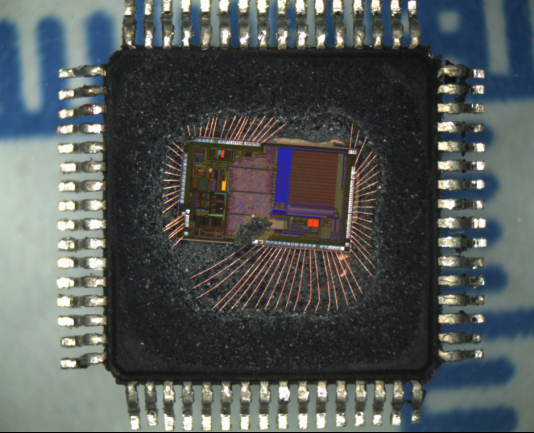
 Attack Microchip PIC18F45K40T Controller Memory
Attack Microchip PIC18F45K40T Controller Memory is a process to unlock microcontroller pic18f45k40t security fuse bit, and then readout flash memory software from microprocessor pic18f45k40t chipset;
On boards with power traces running longer than six inches in length, it is suggested to use a tank capac- itor for integrated circuits, including microcontrollers, to supply a local power source.
The value of the tank capacitor should be determined based on the trace resistance that connects the power supply source to the device, and the maximum current drawn by the device in the application. In other words, select the tank capacitor so that it meets the acceptable voltage sag at the device. Typical values range from 4.7 mF to 47 mF.
ataque Microchip PIC18F45K40T controlador de memoria es un proceso para desbloquear microcontrolador pic18f45k40t bit fusible de seguridad, y luego leer el software de memoria flash del microprocesador pic18f45k40t chipset
The first five events will cause a device Reset. The last one event is considered a continuation of program execution. To determine whether a device Reset or wake-up event occurred, refer to “Determining the Cause of a Reset” when recover microchip pic18f24k22 locked flash memory code.
When the SLEEP instruction is being executed, the next instruction (PC + 2) is prefetched. For the device to wake-up through an interrupt event, the corresponding Interrupt Enable bit must be enabled, as well as the Peripheral Interrupt Enable bit (PEIE = 1), for every interrupt not in PIR0.
Wake-up will occur regardless of the state of the GIE bit. If the GIE bit is disabled, the device continues execution at the instruction after the SLEEP instruction. If the GIE bit is enabled by restoring microcontroller pic18f25k22 memory heximal file, the device executes the instruction after the SLEEP instruction, the device will then call the Interrupt Service Routine.
In cases where the execution of the instruction following SLEEP is not desirable, the user should have a NOP after the SLEEP instruction.
Reverse Engineering PIC18F24K40T Microcontroller Heximal Data
Reverse Engineering PIC18F24K40T Microcontroller Heximal Data is a process to crack pic18f24k40t mcu security fuse bit, and then readout secured code from microprocessor pic18f24k40t flash memory;
The PIC18F24K40T devices contain circuitry to prevent clocking “glitches” when switching between clock sources. A short pause in the system clock occurs during the clock switch.
The length of this pause is between eight and nine clock periods of the new clock source. This ensures that the new clock source is stable and that its pulse width will not be less than the shortest pulse width of the two clock sources.
When the device executes a SLEEP instruction, the system is switched to one of the power managed modes, depending on the state of the IDLEN and SCS1:SCS0 bits of the OSCCON register when recover microcontroller pic18f24k20 flash program and eeprom data.
ingeniería inversa PIC18F24K40T microcontrolador de datos heximales es un proceso para romper pic18f24k40t mcu fusible de seguridad de bits, y luego leer el código de seguridad del microprocesador pic18f24k40t memoria flash
When PRI_IDLE mode is selected, the designated primary oscillator continues to run without interruption. For all other power managed modes, the oscillator using the OSC1 pin is disabled. The OSC1 pin (and OSC2 pin, if used by the oscillator) will stop oscillating.
In Secondary Clock modes (SEC_RUN and SEC_I- DLE), the Timer1 oscillator is operating and providing the system clock in the process of pic18f24k22 mcu locked code recovery. The Timer1 oscillator may also run in all power managed modes if required to clock Timer1 or Timer3.
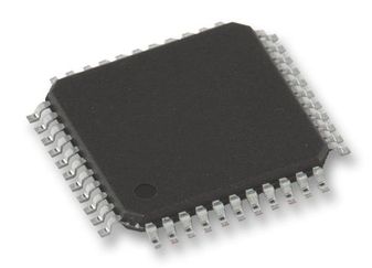
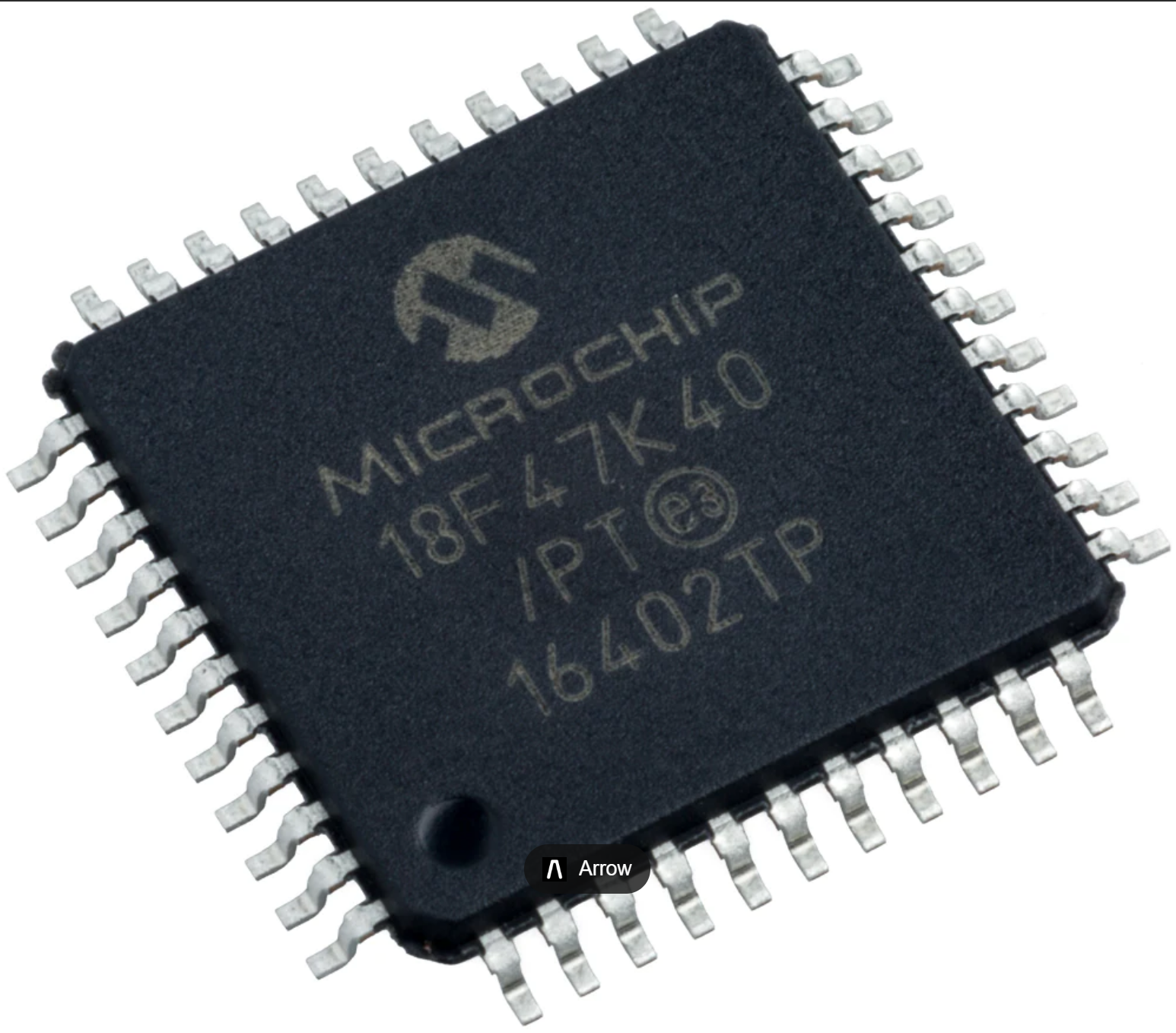
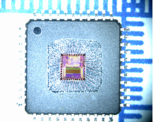
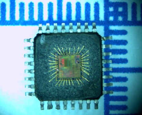
Break Microchip PIC18F47K40T Controller Flash Content
Break Microchip PIC18F47K40T Controller Flash Content needs to hack tamper resistance system of PIC18F47K40T mcu flash memory, and then extract code from pic18f47k40t microprocessor, in the format of binary or heximal;
The IOFS bit when the internal oscillator block has stabilized and is providing the system clock in RC Clock modes or during Two-Speed Start-ups. The T1RUN bit (T1CON<6>) indicates when the Timer1 oscillator is providing the system clock in Secondary Clock modes.
In power managed modes, only one of these three bits will be set at any time. If none of these bits are set, the INTRC is providing the system clock, or the internal oscillator block has just started and is not yet stable when replicate pic18f46k20 microprocessor flash program. The IDLEN bit controls the selective shutdown of the controller’s CPU in power managed modes.
1: The Timer1 oscillator must be enabled to select the secondary clock source. The Timer1 oscillator is enabled by setting the T1OSCEN bit in the Timer1 Control reg- ister (T1CON<3>) to break pic18f46k22 mcu flash heximal memory. If the Timer1 oscillator is not enabled, then any attempt to select a secondary clock source when executing a SLEEP instruction will be ignored.
romper Microchip PIC18F47K40T controlador de contenido flash necesita para hackear sistema de resistencia a la manipulación de PIC18F47K40T mcu memoria flash, y luego extraer el código de pic18f47k40t microprocesador, en el formato de binario o heximal
2: It is recommended that the Timer1 oscil- lator be operating and stable before exe- cuting the SLEEP instruction or a very long delay may occur while the Timer1 oscillator starts.
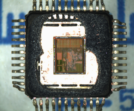
Attack Locked Microprocessor PIC18F2620T Tamper Resistance System
Attack Locked Microprocessor PIC18F2620T Tamper Resistance System and retrieve embedded firmware from microcontroller pic18f2620t flash and eeprom memory, copy encrypted content to new pic18f2620t mcu;
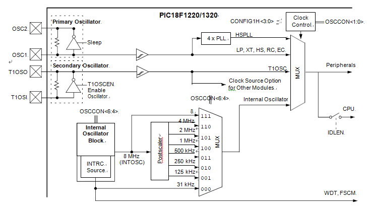
The OSCCON register (Register 2-2) controls several aspects of the system clock’s operation, both in full- power operation and in power managed modes.
The System Clock Select bits, SCS1:SCS0, select the clock source that is used when the device is operating in power managed modes. The available clock sources are the primary clock (defined in Configuration Register 1H) to restore flash memory content from pic18f1220t microprocessor, the secondary clock (Timer1 oscillator) and the internal oscillator block.
The clock selection has no effect until a SLEEP instruction is executed and the device enters a power managed mode of operation. The SCS bits are cleared on all forms of Reset.
The Internal Oscillator Select bits, IRCF2:IRCF0, select the frequency output of the internal oscillator block that is used to drive the system clock. The choices are the INTRC source, the INTOSC source (8 MHz), or one of the six frequencies derived from the INTOSC posts- caler (125 kHz to 4 MHz).
ataque bloqueado microprocesador PIC18F2620T sistema de resistencia a la manipulación y recuperar firmware incrustado del microcontrolador pic18f2620t flash y memoria eeprom, copiar contenido cifrado al nuevo MCU pic18f2620t
If the internal oscillator block is supplying the system clock, changing the states of these bits will have an immediate change on the inter- nal oscillator’s output by decrypting pic18f1230 microcontroller flash memory firmware. The OSTS, IOFS and T1RUN bits indicate which clock source is currently providing the system clock.
The OSTS indicates that the Oscillator Start-up Timer has timed out and the primary clock is providing the system clock in Primary Clock modes. The IOFS bit indicates
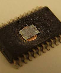
Microchip PIC18F8520 MCU Protection Breaking
The final purpose of Microchip PIC18F8520 MCU Protection Breaking is to extract embedded program from microcontroller pic18f8520, the process of dumping flash heximal and eeprom binary from microprocessor pic18f8520 will be aggressive…
PIC18F8520 devices offer only the Timer1 oscillator as a secondary oscillator. This oscillator, in all power managed modes, is often the time base for functions such as a real-time clock when decoding microcontroller pic18f1220 program from its flash memory.
Most often, a 32.768 kHz watch crystal is connected between the RB6/T1OSO and RB7/T1OSI pins. Like the LP mode oscillator circuit, loading capacitors are also connected from each pin to ground. These pins are also used during ICSP operations.
The Timer1 oscillator is discussed in greater detail in
Section 12.2 “Timer1 Oscillator”.
In addition to being a primary clock source, the internal oscillator block is available as a power managed mode clock source to decap pic18f1320 microchip processor memory. The INTRC source is also used as the clock source for several special features, such as the WDT and Fail-Safe Clock Monitor.
el propósito final de la ruptura de la protección del MCU PIC18F8520 del microchip es extraer el programa incrustado del microcontrolador pic18f8520, el proceso de volcado de flash heximal y eeprom binario del microprocesador pic18f8520 será agresivo
The clock sources for the PIC18F1220/1320 devices are shown in Figure 2-8. See Section 12.0 “Timer1 Module” for further details of the Timer1 oscillator. See Section 19.1 “Configuration Bits” for Configuration register details.
Secured Microcontroller PIC18F4610 Flash Heximal Restoring
Secured Microcontroller PIC18F4610 Flash Heximal Restoring needs to crack mcu pic18f4610 security fuse bit, and then extract embedded firmware from pic18f4610 processor flash memory;
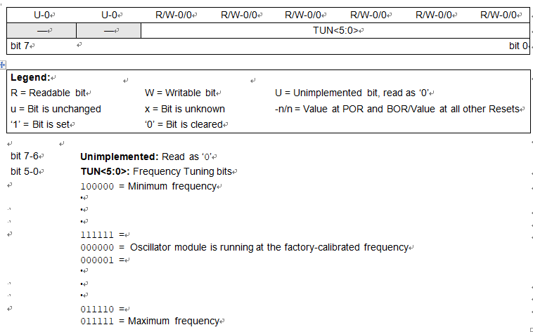
When the OSCTUNE register is modified, the INTOSC and INTRC frequencies will begin shifting to the new frequency. The INTRC clock will reach the new frequency within 8 clock cycles (approximately 8* 32 ms = 256 ms).
The INTOSC clock will stabilize within 1 ms. Code execution continues during this shift. There is no indication that the shift has occurred. Operation of features that depend on the INTRC clock source frequency, such as the WDT, Fail-Safe Clock Monitor and peripherals, will also be affected by the change in frequency.
Like previous PIC18 devices, the PIC18F4610 devices include a feature that allows the system clock source to be switched from the main oscillator to an alternate low-frequency clock source when crack pic18f4550 microcontroller flash memory. PIC18F4610 devices offer two alternate clock sources. When enabled, these give additional options for switching to the various power managed operating modes.
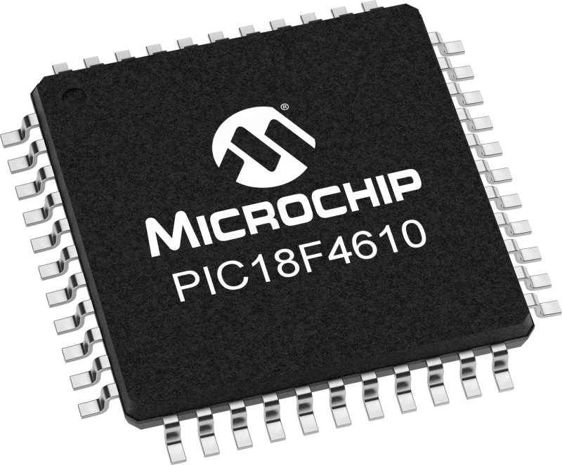
microcontrolador seguro PIC18F4610 flash heximal restauración necesita descifrar MCU pic18f4610 bit de fusible de seguridad, y luego extraer firmware incrustado de la memoria flash del procesador pic18f4610
Essentially, there are three clock sources for these devices:
- Primary oscillators
- Secondary oscillators
- Internal oscillator block
The primary oscillators include the External Crystal and Resonator modes, the External RC modes, the External Clock modes and the internal oscillator block in the process of copying binary file from pic18f458 mcu. The particular mode is defined on POR by the contents of Configuration Register 1H.
The details of these modes are covered earlier in this chapter. The secondary oscillators are those external sources not connected to the OSC1 or OSC2 pins. These sources may continue to operate even after the controller is placed in a power managed mode.
Clone Microchip PIC16LF84 Controller Firmware
Clone Microchip PIC16LF84 Controller Firmware from its locked processor’s flash and eeprom memory, and decode embedded firmware from secured MCU pic16lf84;
Using the internal oscillator as the clock source can eliminate the need for up to two external oscillator pins, which can then be used for digital I/O. Two distinct configurations are available:
- In INTIO1 mode, the OSC2 pin outputs FOSC/4, while OSC1 functions as RA7 for digital input and output.
- In INTIO2 mode, OSC1 functions as RA7 and OSC2 functions as RA6, both for digital input and output.
The internal oscillator block is calibrated at the factory to produce an INTOSC output frequency of 8.0 MHz to restore pic18f1220t processor embedded program. This changes the frequency of the INTRC source from its nominal 31.25 kHz.
Peripherals and features that depend on the INTRC source will be affected by this shift in frequency. Once set during factory calibration when decrypting pic18f1230 microcontroller flash memory, the INTRC frequency will remain within ±2% as temperature and VDD change across their full specified operating ranges.
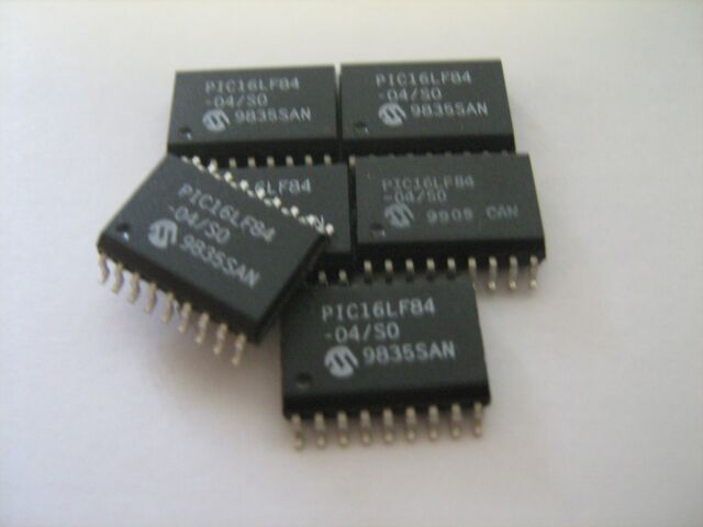
clonar el firmware del controlador PIC16LF84 del microchip de la memoria flash y eeprom de su procesador bloqueado, y decodificar el firmware integrado del MCU pic16lf84 seguro
The internal oscillator’s output has been calibrated at the factory, but can be adjusted in the user’s applica- tion. This is done by writing to the OSCTUNE register. The tuning sensitivity is constant throughout the tuning range.
Reverse PIC18LF2523 Microchip MCU Flash Memory
Reverse PIC18LF2523 Microchip MCU Flash Memory and extract embedded program from microcontroller pic18lf2523 in the format of heximal, the original binary file of pic18lf2523 secured processor will be copied;
In the RC Oscillator mode, the oscillator frequency divided by 4 is available on the OSC2 pin. This signal may be used for test purposes, or to synchronize other logic.
The RCIO Oscillator mode functions like the RC mode, except that the OSC2 pin becomes an additional general purpose I/O pin. The I/O pin becomes bit 6 of PORTA (RA6) is a process of decoding microcontroller pic18f1220 flash program.
The PIC18LF2523 devices include an internal oscillator block, which generates two different clock signals; either can be used as the system’s clock source. This can eliminate the need for external oscillator circuits on the OSC1 and/or OSC2 pins.
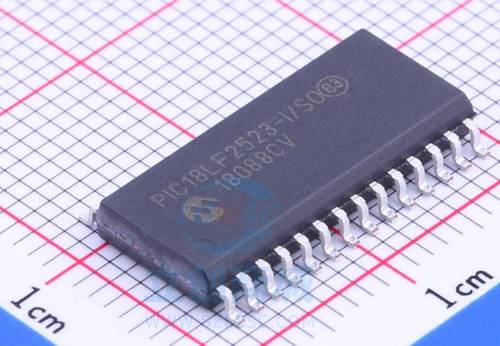
invertir PIC18LF2523 microchip MCU memoria flash y extraer el programa incrustado del microcontrolador pic18lf2523 en el formato de heximal, se copiará el archivo binario original del procesador seguro pic18lf2523
The main output (INTOSC) is an 8 MHz clock source, which can be used to directly drive the system clock. It also drives a postscaler, which can provide a range of clock frequencies from 125 kHz to 4 MHz when decapsulate pic18f1320 processor silicon package. The INTOSC output is enabled when a system clock frequency from 125 kHz to 8 MHz is selected.
The other clock source is the internal RC oscillator (INTRC), which provides a 31 kHz output. The INTRC oscillator is enabled by selecting the internal oscillator block as the system clock source, or when any of the following are enabled:
- Power-up Timer
- Fail-Safe Clock Monitor
- Watchdog Timer
- Two-Speed Start-up
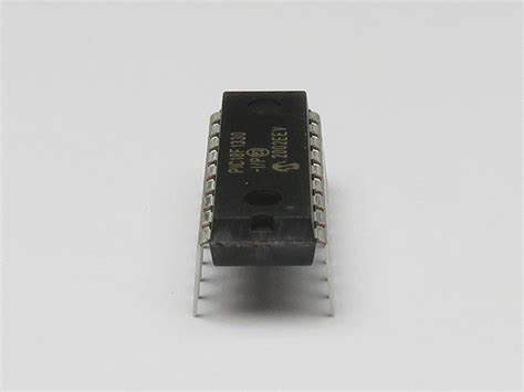
Microprocessor PIC18F1330 Flash Data Recovery
Microprocessor PIC18F1330 Flash Data Recovery needs to unlock encrypted microchip pic18f1330 mcu security fuse bit, and extract locked microchip pic18f1330 mcu heximal file;
The EC and ECIO Oscillator modes require an external clock source to be connected to the OSC1 pin. There is no oscillator start-up time required after a Power-on Reset, or after an exit from Sleep mode.
In the EC Oscillator mode, the oscillator frequency divided by 4 is available on the OSC2 pin. This signal may be used for test purposes, or to synchronize other logic.
The ECIO Oscillator mode functions like the EC mode, except that the OSC2 pin becomes an additional gen- eral purpose I/O pin. The I/O pin becomes bit 6 of PORTA (RA6).
For timing insensitive applications, the “RC” and “RCIO” device options offer additional cost savings . The RC oscillator frequency is a function of the supply voltage when recover pic18f1330 microcontroller code, the resistor (REXT) and capacitor (CEXT) values and the operating temperature.
microprocessador PIC18F1330 recuperação de dados flash precisa desbloquear microchip criptografado pic18f1330 mcu bit fusível de segurança, e extrair microchip bloqueado pic18f1330 mcu arquivo heximal
In addition to this, the oscillator frequency will vary from unit to unit due to normal manufacturing variation. Furthermore, the difference in lead frame capacitance between package types will also affect the oscillation frequency, espe- cially for low CEXT values by . The user also needs to take into account variation, due to tolerance of external R and C components used by breaking microcontroller pic18f14k22 flash memory.
Break Microchip Microcontroller PIC18LF252 Flash Memory
Break Microchip Microcontroller PIC18LF252 Flash Memory and readout embedded program from pic18f252 mcu flash memory, copy program and data to new microprocessor pic18lf252;

Capacitor values are for design guidance only.
These capacitors were tested with the crystals listed below for basic start-up and operation. These values are not optimized.
Different capacitor values may be required to produce acceptable oscillator operation. The user should test the performance of the oscillator over the expected VDD and temperature range for the application. See the notes following this table for additional information.
Note 1: Higher capacitance increases the stability of oscillator, but also increases the start- up time.
2: When operating below 3V VDD, or when using certain ceramic resonators at any voltage, it may be necessary to use the HS mode or switch to a crystal oscillator when recover mcu pic18f252 embedded binary.
3: Since each resonator/crystal has its own characteristics, the user should consult the resonator/crystal manufacturer for appropriate values of external components.
4. RS may be required to avoid overdriving crystals with low drive level specification.
5: Always verify oscillator performance over the VDD and temperature range that is expected for the application.
A Phase Locked Loop (PLL) circuit is provided as an option for users who wish to use a lower frequency crystal oscillator circuit, or to clock the device up to its highest rated frequency from a crystal oscillator to copy microcontroller pic18f252 flash memory. This may be useful for customers who are concerned with EMI due to high-frequency crystals.
quebrar microchip microcontrolador PIC18LF252 memória flash e programa embutido de leitura de pic18f252 mcu memória flash, copiar programa e dados para o novo microprocessador pic18lf252
The HSPLL mode makes use of the HS mode oscillator for frequencies up to 10 MHz. A PLL then multiplies the oscillator output frequency by 4 to produce an internal clock frequency up to 40 MHz. The PLL is enabled only when the oscillator Configura- tion bits are programmed for HSPLL mode. If programmed for any other mode, the PLL is not enabled.